

Comparing Ferroelectric RAM Architectures for Energy-Efficient Computing
MAY 14, 20269 MIN READ
Generate Your Research Report Instantly with AI Agent
PatSnap Eureka helps you evaluate technical feasibility & market potential.
FeRAM Background and Energy Computing Goals
Ferroelectric Random Access Memory (FeRAM) represents a revolutionary non-volatile memory technology that leverages the unique properties of ferroelectric materials to achieve persistent data storage with exceptional energy efficiency. Unlike conventional memory technologies, FeRAM utilizes the spontaneous polarization of ferroelectric crystals, which can be switched between two stable states by applying an external electric field. This fundamental mechanism enables data retention without continuous power supply while maintaining the speed characteristics of volatile memories.
The evolution of FeRAM technology traces back to the 1950s when ferroelectric materials were first explored for memory applications. However, practical implementations emerged in the 1990s with the development of lead zirconate titanate (PZT) thin films and advanced semiconductor fabrication techniques. Early FeRAM devices demonstrated promising characteristics including fast write speeds, low power consumption, and virtually unlimited endurance cycles, positioning them as potential alternatives to traditional SRAM and DRAM technologies.
Contemporary FeRAM architectures have evolved to address the growing demands of energy-efficient computing systems. Modern implementations incorporate advanced ferroelectric materials such as hafnium oxide (HfO2) and bismuth ferrite (BiFeO3), which offer improved scalability and CMOS compatibility. These materials enable the development of high-density memory arrays while maintaining the inherent advantages of ferroelectric switching mechanisms.
The primary energy computing goals driving FeRAM development focus on achieving ultra-low power consumption across all operational modes. Static power reduction represents a critical objective, as FeRAM's non-volatile nature eliminates the need for refresh operations that consume significant energy in conventional DRAM systems. Dynamic power optimization targets the minimization of switching energy during read and write operations through advanced circuit designs and material engineering.
Scalability objectives encompass both dimensional scaling and functional density improvements. Current research emphasizes the development of three-dimensional FeRAM structures and multi-level cell configurations to maximize storage capacity while maintaining energy efficiency. Integration goals focus on seamless compatibility with existing CMOS processes and the development of embedded FeRAM solutions for system-on-chip applications, enabling widespread adoption across diverse computing platforms from IoT devices to high-performance processors.
Market Demand for Energy-Efficient Memory Solutions
The global memory market is experiencing unprecedented demand for energy-efficient solutions, driven by the exponential growth of data-intensive applications and the urgent need to reduce power consumption across computing systems. Traditional memory technologies, particularly DRAM and SRAM, are reaching their physical and economic limits in terms of energy efficiency, creating substantial market opportunities for alternative memory architectures like Ferroelectric RAM.
Data centers represent the largest and most immediate market segment for energy-efficient memory solutions. These facilities consume massive amounts of electricity, with memory subsystems accounting for a significant portion of total power consumption. The increasing deployment of artificial intelligence workloads, machine learning applications, and real-time analytics has intensified the demand for memory systems that can deliver high performance while minimizing energy overhead.
Mobile computing devices constitute another critical market driver, where battery life directly impacts user experience and product competitiveness. Smartphones, tablets, and wearable devices require memory solutions that can maintain performance while extending operational time between charges. The proliferation of Internet of Things devices further amplifies this demand, as these systems often operate in power-constrained environments where energy efficiency is paramount.
Edge computing applications are emerging as a significant growth area, particularly in autonomous vehicles, industrial automation, and smart city infrastructure. These applications require memory systems that can process data locally while operating within strict power budgets. The latency requirements of edge computing make energy-efficient, high-speed memory architectures increasingly valuable.
The automotive sector is driving substantial demand for reliable, energy-efficient memory solutions, especially with the advancement of electric vehicles and autonomous driving systems. These applications require memory technologies that can operate efficiently across wide temperature ranges while maintaining data integrity and minimizing power consumption to preserve battery life.
Enterprise computing environments are increasingly prioritizing total cost of ownership considerations, where energy consumption directly impacts operational expenses. Organizations are actively seeking memory solutions that can reduce cooling requirements and electricity costs while maintaining or improving system performance, creating strong market pull for innovative memory architectures like Ferroelectric RAM.
Current FeRAM Architecture Status and Challenges
Ferroelectric RAM technology has reached a significant maturity level in the semiconductor memory landscape, with several distinct architectural approaches demonstrating commercial viability. The current FeRAM ecosystem primarily revolves around three main architectural paradigms: 1T1C (one transistor, one capacitor), crossbar arrays, and embedded configurations integrated within logic processes. Each architecture exhibits unique characteristics in terms of scalability, power consumption, and manufacturing complexity.
The 1T1C architecture represents the most established approach, successfully implemented by companies like Fujitsu, Cypress, and Rohm. This configuration utilizes ferroelectric capacitors paired with access transistors, enabling non-volatile storage with fast read/write operations typically completing within 100 nanoseconds. Current commercial implementations achieve densities up to 8Mb with operating voltages ranging from 1.8V to 3.3V, demonstrating endurance capabilities exceeding 10^12 write cycles.
Crossbar architectures have emerged as promising alternatives for higher density applications, leveraging ferroelectric materials in resistive switching configurations. These structures eliminate the need for individual capacitors by utilizing the ferroelectric material's polarization states directly within crosspoint arrays. However, scalability challenges persist due to sneak current paths and the requirement for sophisticated selector devices to maintain data integrity in large arrays.
Manufacturing challenges constitute a primary obstacle across all FeRAM architectures. The integration of ferroelectric materials, particularly lead zirconate titanate (PZT), introduces significant process complexity due to material compatibility issues with standard CMOS fabrication. Hydrogen sensitivity during backend processing can degrade ferroelectric properties, necessitating specialized encapsulation techniques and modified process flows that increase manufacturing costs substantially.
Scaling limitations present another critical challenge, as ferroelectric capacitors face fundamental physical constraints when approaching sub-100nm dimensions. Depolarization effects become increasingly problematic at smaller scales, potentially compromising data retention characteristics. Additionally, the relatively large cell sizes compared to conventional DRAM or Flash memory limit FeRAM's competitiveness in high-density applications.
Power consumption profiles vary significantly among different FeRAM architectures. While standby power consumption remains exceptionally low due to non-volatile characteristics, active power during read/write operations can be substantial, particularly in crossbar configurations requiring higher switching voltages. Current implementations typically consume 2-5mA during active operations, with standby currents below 10μA.
Temperature stability and data retention represent ongoing technical challenges, especially for automotive and industrial applications requiring extended temperature ranges. Most current FeRAM devices guarantee data retention for 10 years at 85°C, but performance degradation accelerates at higher temperatures, limiting deployment in extreme environments.
The competitive landscape reveals geographical concentration, with Japanese manufacturers maintaining technological leadership in traditional 1T1C architectures, while emerging players focus on novel crossbar and embedded solutions. Cost considerations remain prohibitive for many applications, with FeRAM pricing typically 10-50 times higher than equivalent EEPROM solutions, constraining market adoption despite superior performance characteristics.
Existing FeRAM Architecture Solutions
01 Low-power ferroelectric memory cell design
Ferroelectric RAM energy efficiency can be improved through optimized memory cell architectures that reduce power consumption during read and write operations. These designs focus on minimizing leakage current and reducing the voltage required for switching ferroelectric materials. Advanced cell structures incorporate specialized transistor configurations and capacitor designs to achieve lower operating voltages while maintaining data retention capabilities.- Low-power ferroelectric memory cell design: Ferroelectric RAM energy efficiency can be improved through optimized memory cell architectures that reduce power consumption during read and write operations. These designs focus on minimizing leakage current and reducing the voltage required for switching ferroelectric capacitors. Advanced cell structures incorporate transistor configurations that enable lower operating voltages while maintaining data retention capabilities.
- Power management and control circuits: Energy efficiency in ferroelectric memory systems is enhanced through sophisticated power management circuits that control voltage supply and timing operations. These circuits implement dynamic voltage scaling, power gating techniques, and optimized charge pump designs to reduce overall power consumption. The control systems manage standby modes and active operation states to minimize energy waste.
- Ferroelectric material optimization: The development of advanced ferroelectric materials with improved switching characteristics contributes significantly to energy efficiency. These materials exhibit lower coercive voltages, faster switching speeds, and reduced fatigue properties. Material engineering focuses on crystal structure modifications and doping techniques to achieve optimal polarization switching with minimal energy requirements.
- Write and read operation optimization: Energy efficiency improvements are achieved through optimized write and read operation protocols that minimize the energy required for data access. These techniques include pulse width optimization, voltage level adjustment, and timing sequence refinement. Advanced sensing circuits and reference voltage generation methods reduce the power needed for reliable data detection and storage operations.
- System-level energy management: Comprehensive energy efficiency solutions involve system-level approaches that integrate multiple power-saving techniques across the entire ferroelectric memory architecture. These include hierarchical power domains, adaptive refresh mechanisms, and intelligent data management algorithms. The systems implement predictive power management and workload-aware optimization to achieve maximum energy efficiency while maintaining performance requirements.
02 Ferroelectric material optimization for energy reduction
Energy efficiency improvements are achieved through the development of advanced ferroelectric materials with lower coercive fields and reduced switching energy requirements. These materials enable faster switching speeds while consuming less power, and they maintain stable polarization states with minimal energy loss. The optimization includes crystal structure modifications and doping techniques to enhance the ferroelectric properties.Expand Specific Solutions03 Power management and control circuits
Sophisticated power management systems are implemented to control the energy consumption of ferroelectric memory arrays. These circuits include voltage regulators, charge pumps, and timing control units that optimize power delivery during different operational modes. The systems can dynamically adjust power levels based on memory access patterns and implement sleep modes to reduce standby power consumption.Expand Specific Solutions04 Write and read operation energy optimization
Energy efficiency is enhanced through optimized write and read operation protocols that minimize the energy required for data access. These techniques include pulse shaping methods, selective writing schemes, and read sensing amplifiers with improved sensitivity. The optimization reduces the overall energy per bit operation while maintaining reliable data storage and retrieval performance.Expand Specific Solutions05 Array architecture and peripheral circuit efficiency
Energy consumption is reduced through efficient array architectures and peripheral circuit designs that minimize parasitic effects and optimize signal routing. These designs include hierarchical memory structures, efficient address decoding schemes, and low-power sense amplifiers. The architecture improvements focus on reducing the capacitive loading and minimizing the energy required for data line charging and discharging during memory operations.Expand Specific Solutions
Key Players in FeRAM and Memory Industry
The ferroelectric RAM (FeRAM) market represents an emerging segment within the broader memory semiconductor industry, currently in its early commercialization phase with significant growth potential driven by increasing demand for energy-efficient computing solutions. The market remains relatively niche compared to traditional memory technologies, with estimated global revenues in the hundreds of millions, but shows promising expansion prospects as IoT and edge computing applications proliferate. Technology maturity varies significantly across market participants, with established semiconductor giants like Samsung Electronics, SK Hynix, and Micron Technology leveraging their advanced manufacturing capabilities and R&D resources to develop next-generation FeRAM architectures. Companies such as Intel, IBM, and Texas Instruments are actively pursuing innovative approaches to integrate ferroelectric materials into their existing product portfolios, while specialized firms like Kepler Computing focus exclusively on breakthrough ferroelectric computing technologies. Research institutions including Tsinghua University and Forschungszentrum Jülich contribute fundamental advances in materials science and device physics, supporting the overall technological progression toward commercially viable, high-density FeRAM solutions for energy-efficient computing applications.
Texas Instruments Incorporated
Technical Solution: Texas Instruments has developed ferroelectric RAM architectures specifically optimized for ultra-low power microcontroller and embedded applications. Their FeRAM technology utilizes lead zirconate titanate (PZT) ferroelectric capacitors in a 2T-2C differential architecture that provides excellent noise immunity and data integrity. TI's approach features operating currents as low as 150nA during standby mode and write energies 10,000x lower than EEPROM, enabling battery-powered devices to operate for years without replacement. The architecture supports instant-on capability with zero boot time, fast write speeds of 125ns, and operates across extended temperature ranges from -40°C to 85°C, making it ideal for industrial IoT and automotive applications.
Strengths: Proven reliability in harsh environments, excellent power efficiency for embedded systems. Weaknesses: Limited density compared to other non-volatile memories, higher cost per bit.
Samsung Electronics Co., Ltd.
Technical Solution: Samsung has developed innovative ferroelectric RAM architectures based on hafnium zirconium oxide (HfZrO2) ferroelectric materials integrated into their advanced semiconductor processes. Their FeRAM technology features a 1T-1C (one transistor, one capacitor) architecture optimized for energy efficiency, achieving write power consumption 100x lower than conventional DRAM. Samsung's approach incorporates advanced ferroelectric capacitor designs with optimized electrode materials and interface engineering to enhance polarization switching efficiency. The architecture supports operating voltages as low as 0.8V and demonstrates excellent scalability down to sub-10nm technology nodes, making it suitable for next-generation energy-efficient computing systems and IoT applications.
Strengths: Advanced process technology integration, excellent scalability to smaller nodes. Weaknesses: Complex manufacturing requirements, potential reliability challenges at extreme scaling.
Core FeRAM Architecture Innovations
Semiconductor device having ferroelectic memory cells and method of manufacturing the same
PatentInactiveUS6759251B2
Innovation
- The semiconductor device design includes forming plug electrodes and lower electrodes from oxidization-resistant materials, with wiring and contacts connecting upper and lower electrodes without exposing source/drain regions to high-temperature oxidizing atmospheres, allowing for effective annealing and improving ferroelectric film characteristics.


Ferroelectric random access memory
PatentInactiveUS20160086648A1
Innovation
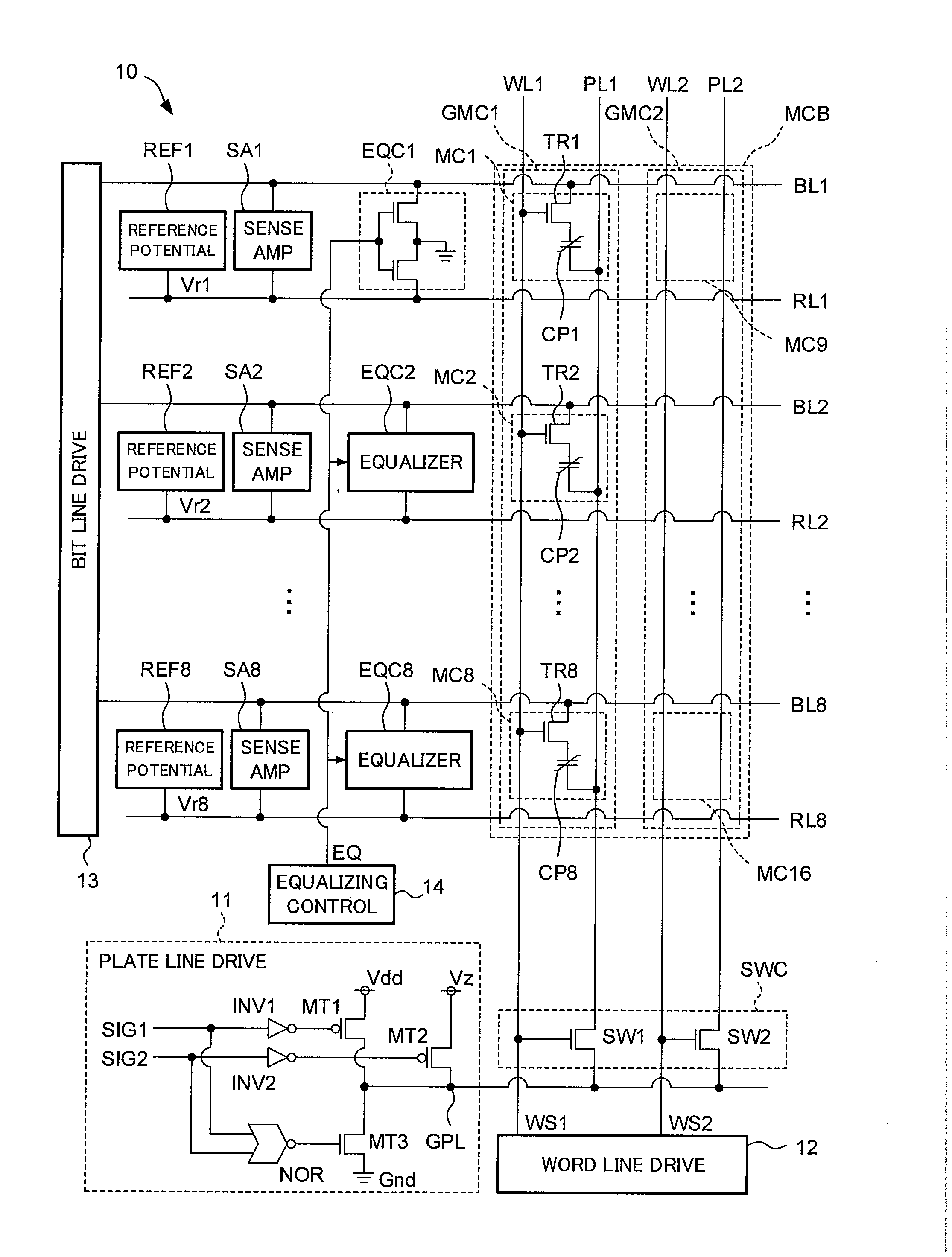
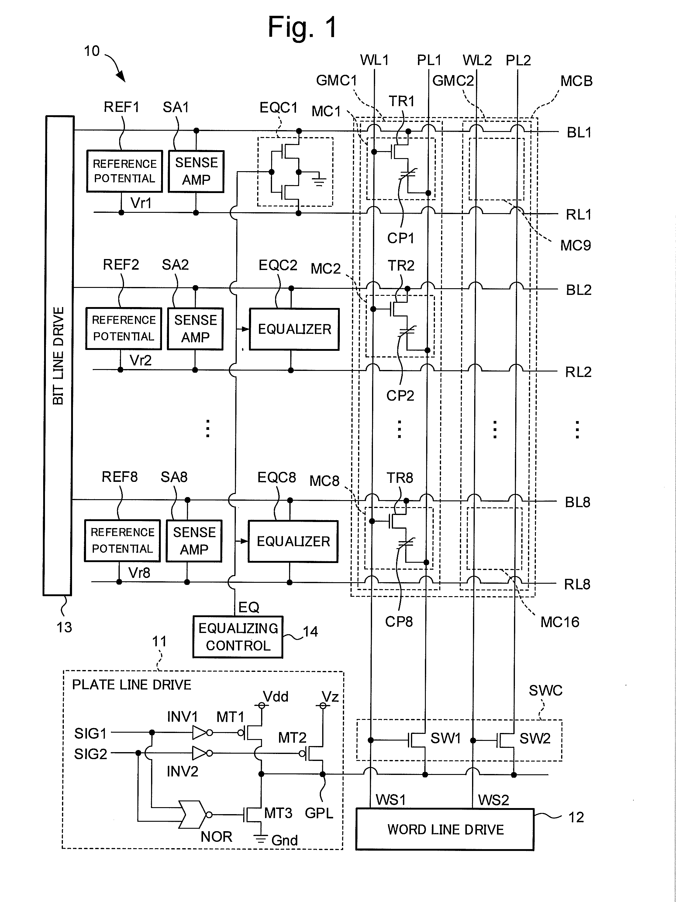
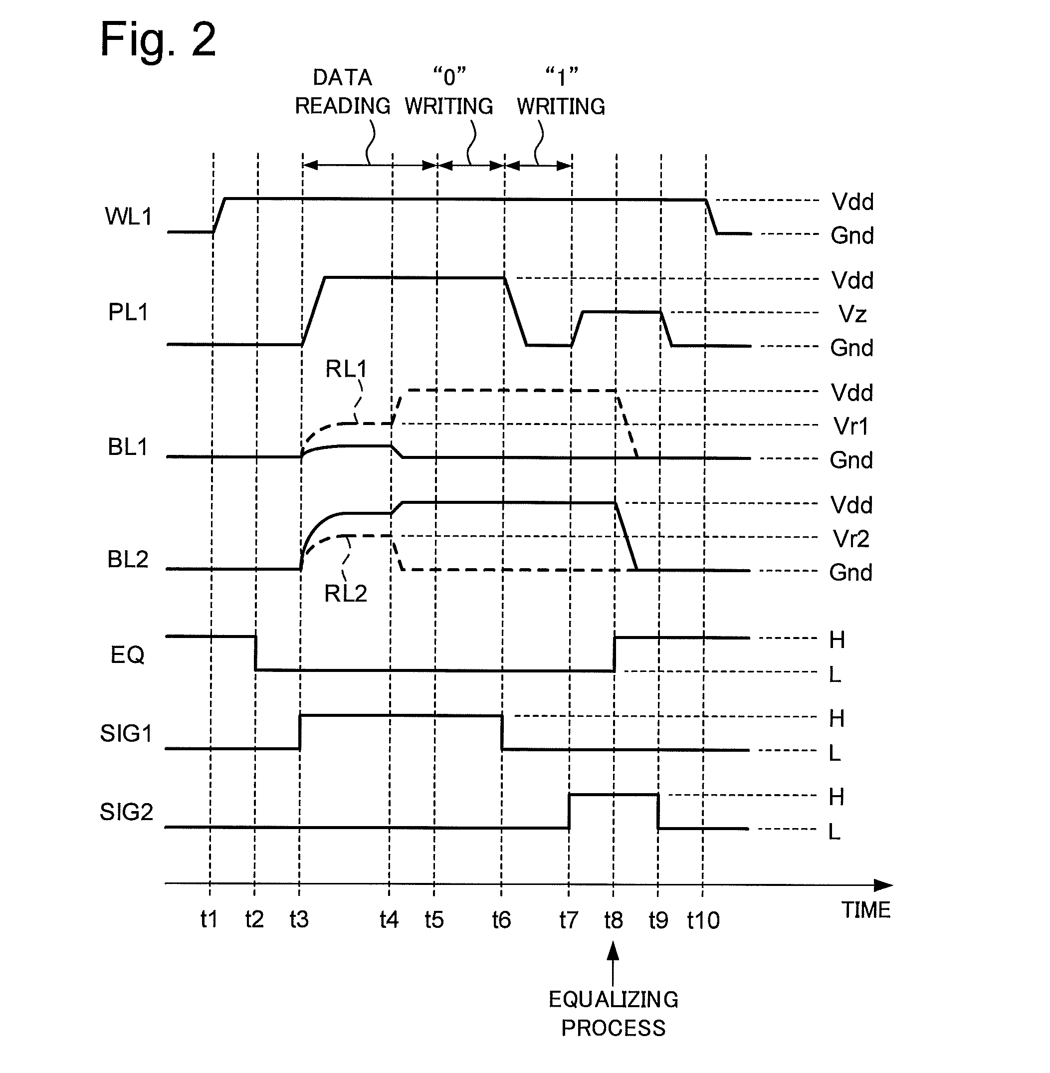
- A FeRAM configuration with a memory cell matrix of 1T1C type memory cells connected to paired word and plate lines, utilizing a plate line drive circuit that applies a noise absorption potential between the ground and power source potentials to the plate line before an equalizing process, thereby reducing the effect of potential variation on residual polarization values.

FeRAM Manufacturing Process Considerations
The manufacturing of Ferroelectric RAM presents unique challenges that significantly impact both production costs and device performance characteristics. Unlike conventional semiconductor memory technologies, FeRAM fabrication requires specialized processes to handle ferroelectric materials while maintaining their critical polarization properties throughout the manufacturing cycle.
The ferroelectric capacitor formation represents the most critical aspect of FeRAM manufacturing. Lead zirconate titanate (PZT) remains the dominant ferroelectric material, requiring deposition temperatures between 550-650°C. This thermal budget creates integration challenges with standard CMOS processes, as high temperatures can degrade previously formed transistor characteristics. Alternative materials like hafnium oxide (HfO2) offer lower processing temperatures around 400°C, enabling better CMOS compatibility but often at the cost of reduced ferroelectric properties.
Electrode selection and deposition critically influence device reliability and endurance. Platinum-based electrodes provide excellent chemical stability and low reactivity with ferroelectric materials, but their high cost and complex etching requirements increase manufacturing complexity. Conductive oxides like iridium oxide or ruthenium oxide offer cost advantages while maintaining adequate performance, though they may exhibit higher leakage currents under certain operating conditions.
The crystallization annealing process determines the final ferroelectric properties and requires precise temperature and atmosphere control. Oxygen partial pressure during annealing affects oxygen vacancy concentration, directly impacting retention characteristics and endurance cycling. Manufacturing facilities must implement specialized furnace systems with precise gas flow control to achieve consistent ferroelectric properties across wafer lots.
Etching and patterning of ferroelectric stacks present additional challenges due to the chemical resistance of ferroelectric materials. Ion beam etching or reactive ion etching with chlorine-based chemistries are typically employed, but these processes can create sidewall damage that degrades switching characteristics. Post-etch cleaning and recovery annealing steps are often necessary to restore optimal ferroelectric behavior.
Yield considerations become particularly important given the additional process complexity. Ferroelectric materials are sensitive to contamination, requiring enhanced cleanroom protocols and specialized handling procedures. The integration of ferroelectric processing with standard CMOS fabrication often necessitates hybrid manufacturing approaches, where ferroelectric modules are processed separately and then integrated, increasing overall production costs but improving yield predictability.
Energy Efficiency Benchmarking Standards
The establishment of standardized energy efficiency benchmarking frameworks for ferroelectric RAM architectures represents a critical need in the semiconductor industry. Current evaluation methodologies lack uniformity, making it challenging to conduct meaningful comparisons between different FeRAM implementations. The absence of standardized metrics has led to fragmented assessment approaches, where manufacturers often employ proprietary testing protocols that may not accurately reflect real-world performance scenarios.
Industry organizations such as JEDEC and IEEE have begun developing preliminary standards for non-volatile memory energy assessment, but these frameworks require significant refinement to address the unique characteristics of ferroelectric technologies. The complexity arises from FeRAM's distinctive switching mechanisms, which exhibit different energy consumption patterns compared to traditional memory technologies. Standardization efforts must account for variables including operating voltage ranges, switching frequencies, and temperature dependencies that directly impact energy efficiency measurements.
Comprehensive benchmarking standards should encompass multiple operational scenarios, including active read/write operations, standby power consumption, and retention energy requirements. The standards must define specific test conditions, measurement methodologies, and reporting formats to ensure reproducible results across different testing environments. Critical parameters include switching energy per bit, leakage current specifications, and endurance-related energy degradation metrics.
The development of these standards requires collaboration between memory manufacturers, system integrators, and standardization bodies to establish universally accepted testing protocols. Proposed frameworks should incorporate both static and dynamic power measurements, considering real-world application patterns such as cache operations, data logging, and embedded system requirements. Additionally, the standards must address scaling considerations, as energy efficiency characteristics may vary significantly between different FeRAM cell architectures and manufacturing processes.
Implementation of robust benchmarking standards will enable more accurate performance comparisons, facilitate technology selection decisions, and drive innovation toward more energy-efficient ferroelectric memory solutions. These standards will ultimately support the broader adoption of FeRAM technologies in energy-constrained computing applications.
Unlock deeper insights with PatSnap Eureka Quick Research — get a full tech report to explore trends and direct your research. Try now!
Generate Your Research Report Instantly with AI Agent
Supercharge your innovation with PatSnap Eureka AI Agent Platform!