

Comparing Neuromorphic Sensor Architectures for Scalability
JUN 5, 20269 MIN READ
Generate Your Research Report Instantly with AI Agent
PatSnap Eureka helps you evaluate technical feasibility & market potential.
Neuromorphic Sensor Evolution and Scalability Goals
Neuromorphic sensor technology emerged from the convergence of neuroscience and semiconductor engineering in the late 20th century, drawing inspiration from biological neural networks' efficiency in processing sensory information. The foundational work began in the 1980s with Carver Mead's pioneering research on analog VLSI implementations of neural functions, which established the theoretical framework for event-driven sensing architectures that mimic retinal and cochlear processing mechanisms.
The evolution trajectory has progressed through distinct phases, starting with basic silicon retina implementations in the 1990s, advancing to dynamic vision sensors in the 2000s, and culminating in today's sophisticated multi-modal neuromorphic sensing platforms. Each developmental stage has addressed fundamental limitations in temporal resolution, power consumption, and data throughput that constrained previous generations of conventional frame-based sensors.
Contemporary neuromorphic sensor architectures face unprecedented scalability demands driven by edge computing applications, autonomous systems, and Internet of Things deployments. The primary scalability goals encompass achieving sub-milliwatt power consumption while maintaining microsecond-level temporal precision, supporting pixel arrays exceeding megapixel densities, and enabling real-time processing of asynchronous event streams without computational bottlenecks.
Integration scalability represents another critical objective, focusing on seamless incorporation of neuromorphic sensors into existing digital processing pipelines while preserving their inherent advantages of sparse data representation and event-driven operation. This requires developing standardized interfaces and communication protocols that can efficiently handle the variable data rates characteristic of neuromorphic sensor outputs.
Manufacturing scalability goals target cost-effective production using standard CMOS processes, enabling widespread commercial adoption across diverse application domains. The challenge lies in optimizing circuit designs for yield and reliability while maintaining the analog precision necessary for neuromorphic functionality, particularly as feature sizes continue to shrink and process variations increase.
System-level scalability objectives emphasize architectural flexibility to accommodate varying computational requirements, from simple edge detection to complex pattern recognition tasks. This involves developing modular sensor designs that can be configured for specific applications while maintaining compatibility with emerging neuromorphic computing platforms and spiking neural network accelerators.
Market Demand for Scalable Neuromorphic Computing Solutions
The global neuromorphic computing market is experiencing unprecedented growth driven by the increasing demand for energy-efficient processing solutions across multiple industries. Traditional von Neumann architectures face significant limitations in handling the massive data volumes generated by Internet of Things devices, autonomous systems, and artificial intelligence applications. This computational bottleneck has created substantial market opportunities for neuromorphic technologies that can process information with dramatically reduced power consumption while maintaining high performance levels.
Edge computing applications represent the largest demand segment for scalable neuromorphic solutions. Smart cities, industrial automation, and autonomous vehicles require real-time processing capabilities at distributed locations where power efficiency and compact form factors are critical. The proliferation of sensor networks in these environments necessitates computing architectures that can scale seamlessly from single-node processing to large distributed systems without proportional increases in energy consumption.
Healthcare and biomedical applications constitute another rapidly expanding market segment. Wearable health monitoring devices, implantable medical systems, and portable diagnostic equipment require ultra-low power consumption while maintaining sophisticated signal processing capabilities. Neuromorphic sensor architectures offer the potential to extend battery life significantly while enabling more complex health monitoring algorithms that can operate continuously without frequent charging cycles.
The automotive industry presents substantial opportunities for scalable neuromorphic computing, particularly in advanced driver assistance systems and autonomous vehicle development. These applications demand real-time processing of multiple sensor inputs including cameras, lidar, and radar systems. Scalable neuromorphic architectures can potentially reduce the computational overhead and power requirements of current automotive processing systems while improving response times for critical safety functions.
Data center operators and cloud service providers are increasingly interested in neuromorphic solutions for specific workloads, particularly those involving pattern recognition, signal processing, and machine learning inference tasks. The potential for significant energy savings in large-scale deployments makes neuromorphic computing attractive for organizations seeking to reduce operational costs and environmental impact while maintaining computational performance standards.
Current Neuromorphic Architectures and Scalability Limitations
Contemporary neuromorphic sensor architectures primarily fall into three distinct categories: event-driven vision sensors, spiking neural network processors, and hybrid analog-digital systems. Event-driven vision sensors, exemplified by Dynamic Vision Sensors (DVS) and DAVIS cameras, capture temporal changes in pixel intensity rather than traditional frame-based imaging. These architectures demonstrate exceptional temporal resolution and power efficiency but face significant scalability challenges when processing high-resolution scenes with dense visual activity.
Spiking neural network processors represent another major architectural approach, incorporating dedicated hardware implementations of leaky integrate-and-fire neurons and synaptic connections. Current implementations like Intel's Loihi and IBM's TrueNorth chips demonstrate promising neuromorphic computing capabilities but encounter substantial limitations in scaling beyond thousands of neurons while maintaining real-time processing requirements.
The scalability bottlenecks in existing neuromorphic architectures stem from several fundamental constraints. Memory bandwidth limitations create significant challenges as the number of synaptic connections scales quadratically with neuron count. Traditional von Neumann architectures struggle with the massive parallel processing demands inherent in neuromorphic computation, leading to energy inefficiencies and processing delays that compound with system size.
Communication overhead presents another critical scalability barrier. As neuromorphic systems expand, the routing complexity for spike-based communication increases exponentially, creating congestion points that degrade overall system performance. Current architectures lack efficient mechanisms for managing inter-neuron communication at scale, resulting in latency issues that undermine the real-time processing advantages neuromorphic systems are designed to provide.
Power consumption scaling represents a particularly challenging limitation for large-scale neuromorphic implementations. While individual neuromorphic components demonstrate superior energy efficiency compared to traditional processors, the cumulative power requirements for maintaining large networks of artificial neurons and synapses often exceed practical deployment thresholds. This constraint becomes especially pronounced in mobile and edge computing applications where power budgets are strictly limited.
Manufacturing precision and yield considerations further complicate scalability efforts. Neuromorphic architectures often rely on analog circuit components that require precise calibration and matching. As chip complexity increases, maintaining consistent performance across all neuromorphic elements becomes increasingly difficult, leading to reduced yields and higher production costs that limit commercial viability for large-scale implementations.
Existing Neuromorphic Sensor Architecture Solutions
01 Hierarchical neuromorphic sensor network architectures
Implementation of multi-layered neuromorphic sensor systems that enable distributed processing and hierarchical data flow. These architectures utilize cascaded processing units that can handle increasing complexity of sensory data while maintaining scalability through modular design approaches. The hierarchical structure allows for efficient resource allocation and parallel processing capabilities.- Distributed neuromorphic processing architectures: Scalable neuromorphic sensor systems utilize distributed processing architectures that enable parallel computation across multiple processing nodes. These architectures implement hierarchical processing structures where sensory data is processed at different levels, from local feature extraction to global pattern recognition. The distributed approach allows for efficient load balancing and reduces communication bottlenecks, enabling the system to scale effectively with increasing sensor density and computational requirements.
- Adaptive network topology for sensor scaling: Neuromorphic sensor architectures employ adaptive network topologies that can dynamically reconfigure based on computational demands and sensor array size. These systems implement self-organizing principles that allow the network structure to evolve and optimize connectivity patterns as the scale increases. The adaptive topology ensures efficient information flow and maintains processing performance regardless of the number of sensors in the array.
- Hierarchical memory management systems: Scalable neuromorphic architectures incorporate hierarchical memory management systems that optimize data storage and retrieval across different processing levels. These systems implement multi-tier memory structures with local, intermediate, and global memory pools that can efficiently handle increasing data volumes. The hierarchical approach enables effective memory utilization and reduces access latency as the sensor network scales up.
- Event-driven processing for scalable computation: Event-driven processing mechanisms enable neuromorphic sensor architectures to achieve scalability by processing information only when significant events occur. This approach reduces computational overhead and power consumption by eliminating unnecessary processing of static or redundant data. The event-driven paradigm allows the system to handle large-scale sensor arrays efficiently while maintaining real-time processing capabilities.
- Modular hardware design for expandable systems: Modular hardware architectures provide the foundation for scalable neuromorphic sensor systems by enabling incremental expansion and reconfiguration. These designs implement standardized interfaces and communication protocols that allow seamless integration of additional sensor modules and processing units. The modular approach facilitates system growth and adaptation to varying application requirements while maintaining architectural coherence and performance optimization.
02 Adaptive scaling mechanisms for neuromorphic processors
Dynamic scaling techniques that adjust neuromorphic processor configurations based on computational demands and available resources. These mechanisms enable real-time optimization of processing capacity, power consumption, and performance metrics. The adaptive nature allows systems to maintain efficiency across varying workload conditions and sensor input complexities.Expand Specific Solutions03 Distributed neuromorphic sensor array integration
Methods for integrating multiple neuromorphic sensors into distributed arrays that can scale across large geographical areas or complex sensing environments. These approaches focus on maintaining coherent data processing while distributing computational load across multiple sensor nodes. The integration techniques ensure seamless communication and coordination between distributed sensing elements.Expand Specific Solutions04 Memory-efficient neuromorphic computation architectures
Architectural designs that optimize memory usage and data storage in neuromorphic sensor systems to support scalability requirements. These approaches implement novel memory hierarchies, data compression techniques, and efficient synaptic weight storage methods. The memory optimization enables larger neural networks and more complex sensor processing capabilities within constrained hardware resources.Expand Specific Solutions05 Modular neuromorphic sensor component design
Development of standardized, interchangeable neuromorphic sensor components that enable flexible system scaling through modular assembly. These designs focus on creating reusable building blocks that can be combined in various configurations to meet specific application requirements. The modular approach facilitates easy expansion, maintenance, and customization of neuromorphic sensor systems.Expand Specific Solutions
Leading Companies in Neuromorphic Computing Industry
The neuromorphic sensor architecture landscape is in an early-to-mid development stage, with the market experiencing rapid growth driven by increasing demand for edge AI and low-power computing solutions. The market size is expanding significantly as applications in autonomous vehicles, IoT devices, and robotics gain traction. Technology maturity varies considerably across players, with established semiconductor giants like Intel, IBM, Samsung, and NVIDIA leading in advanced neuromorphic chip development and system integration capabilities. These companies possess substantial R&D resources and manufacturing expertise, positioning them ahead of emerging specialized firms like Thalchemy Corp. and Camgian Microsystems, which focus on niche neuromorphic algorithms and sensing solutions. Academic institutions including Peking University, Tsinghua University, and KAIST contribute foundational research, while research organizations like Fraunhofer-Gesellschaft and CEA bridge academic discoveries with commercial applications, creating a competitive ecosystem spanning from basic research to commercial deployment.
International Business Machines Corp.
Technical Solution: IBM has developed TrueNorth neuromorphic chip architecture featuring 4096 neurosynaptic cores with 1 million neurons and 256 million synapses, designed for ultra-low power consumption at 70mW during active operation. The architecture implements event-driven asynchronous processing with distributed memory architecture, enabling real-time sensory processing for applications like visual pattern recognition and auditory processing. IBM's approach focuses on scalable tile-based design where multiple chips can be interconnected to create larger neuromorphic systems, supporting up to 16 million neurons per board. The system utilizes spike-based communication protocols and implements local learning algorithms for adaptive behavior in dynamic environments.
Strengths: Proven scalability with tile-based architecture, extremely low power consumption, mature development ecosystem. Weaknesses: Limited commercial availability, complex programming model, restricted to specific application domains.
Intel Corp.
Technical Solution: Intel's Loihi neuromorphic research chip implements 128 neuromorphic cores with 131,072 neurons and 130 million synapses, featuring on-chip learning capabilities through spike-timing-dependent plasticity (STDP). The architecture supports asynchronous event-driven computation with programmable synaptic delays and multiple compartment neuron models. Loihi's scalability is demonstrated through multi-chip configurations supporting up to 16.7 million neurons across 128 chips connected via mesh topology. The system operates at sub-milliwatt power levels and includes embedded x86 cores for conventional processing tasks. Intel's approach emphasizes real-time adaptive learning and supports various neural network topologies including convolutional and recurrent architectures for sensor fusion applications.
Strengths: Advanced on-chip learning capabilities, flexible programming framework, strong research community support. Weaknesses: Still in research phase, limited commercial deployment, requires specialized programming expertise.
Key Patents in Scalable Neuromorphic Design
Scalable free-running neuromorphic computer
PatentInactiveUS20180189632A1
Innovation
- A scalable, free-running neuromorphic processor design that uses pseudo-random number generators to control spiking activity and enable event-driven spike integration, eliminating the need for spike buffers and global synchronization signals by integrating spikes as they arrive between inter-spike intervals.
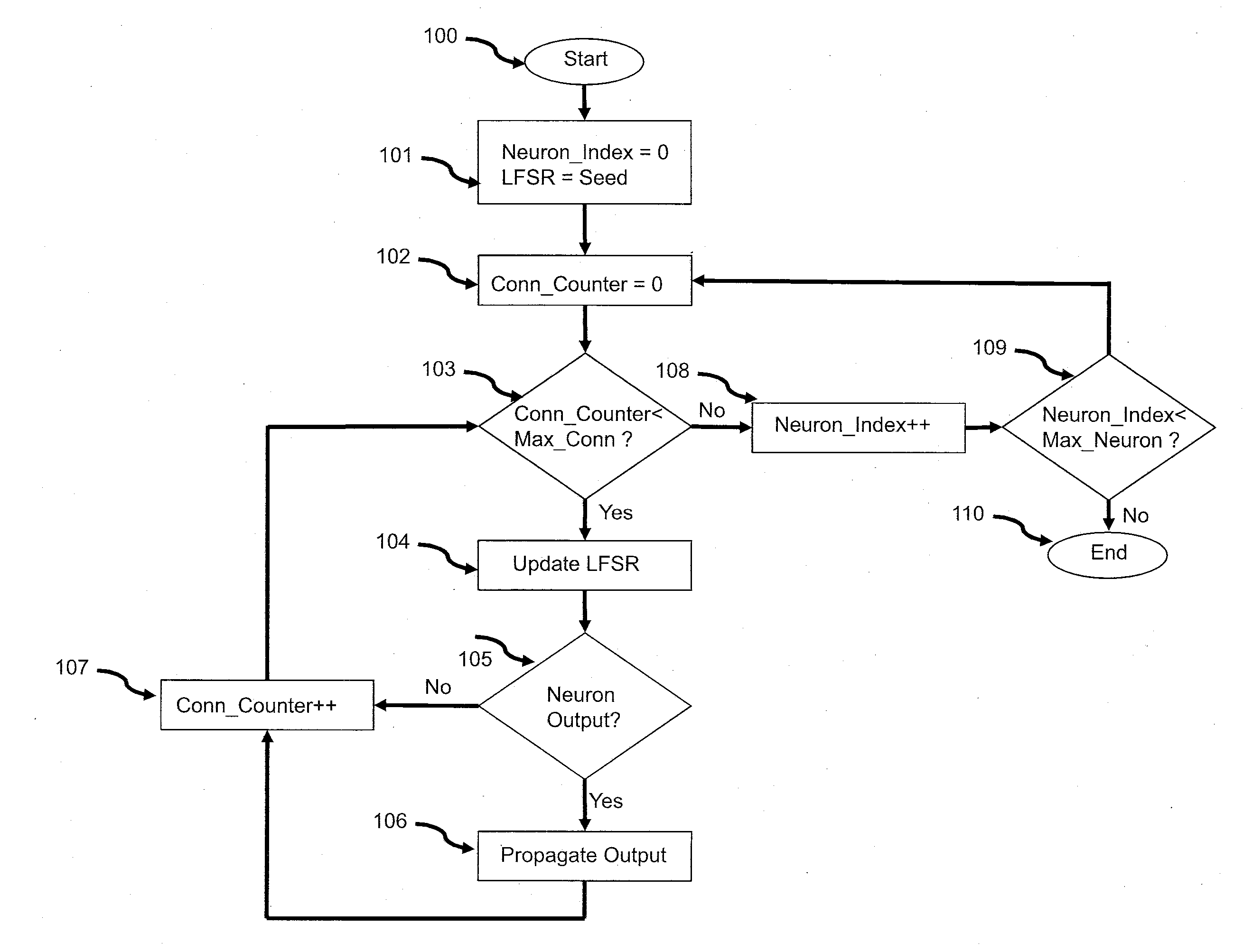
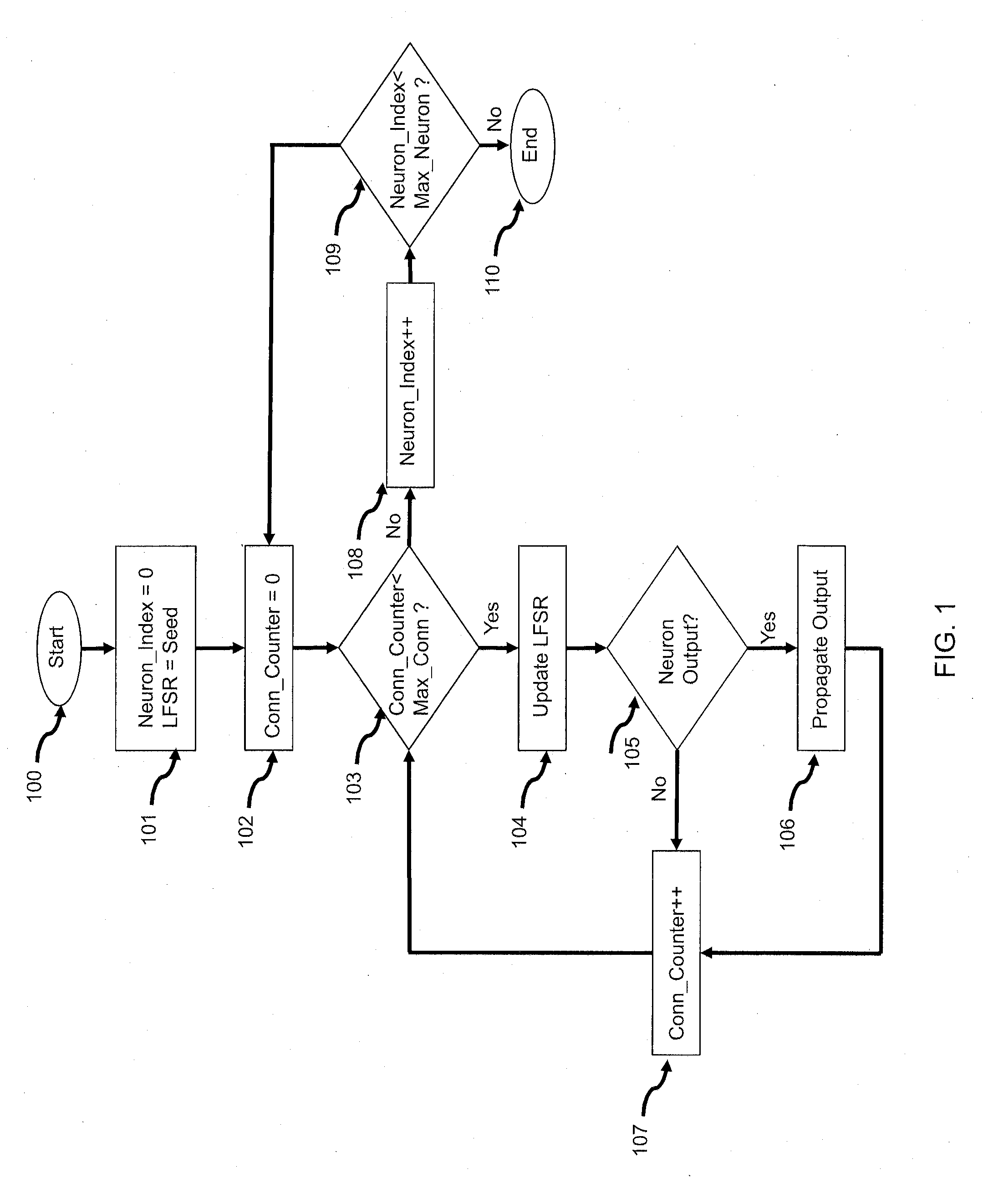
Efficient and scalable systems for calculating neural network connectivity in an event-driven way
PatentActiveUS20160098629A1
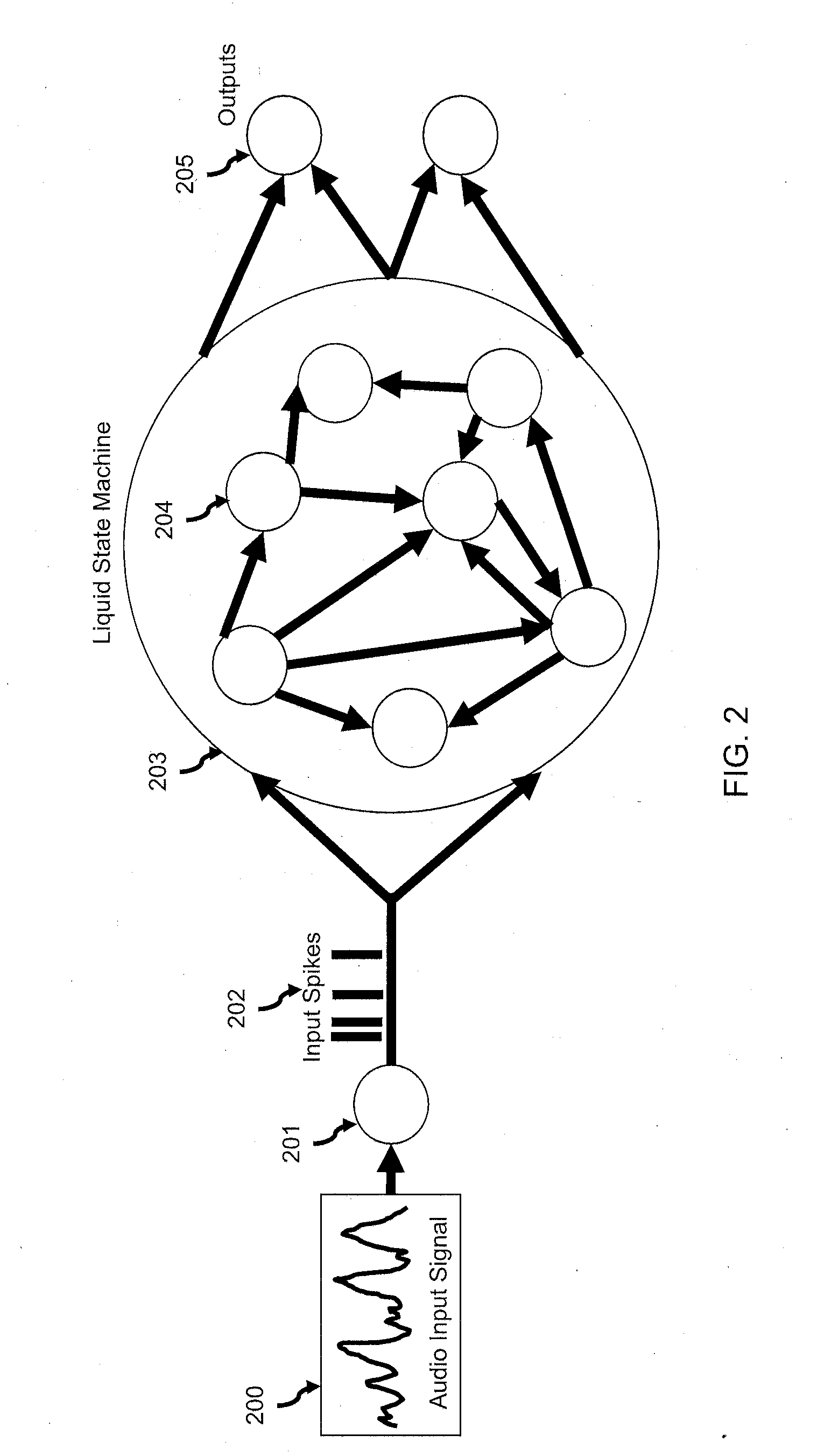
Innovation
- The system calculates neural connectivity and other parameters on-demand using a Linear Feedback Shift Register (LFSR) instead of storing them, allowing for efficient and scalable neural networks that mimic biological connectivity patterns, such as in Liquid State Machines, reducing memory needs and computational overhead.

Hardware Manufacturing Standards for Neuromorphic Chips
The manufacturing of neuromorphic chips requires specialized hardware standards that differ significantly from conventional semiconductor fabrication processes. Current industry standards primarily focus on analog and mixed-signal circuit manufacturing, which forms the foundation for neuromorphic device production. These standards encompass wafer-level processing, device characterization, and quality control metrics specifically tailored for event-driven computing architectures.
Fabrication tolerances represent a critical aspect of neuromorphic chip manufacturing standards. Unlike digital processors that rely on binary switching, neuromorphic devices require precise analog characteristics to emulate neural behavior. Manufacturing standards must accommodate variations in threshold voltages, leakage currents, and timing parameters that directly impact synaptic weight accuracy and spike timing precision. Industry specifications typically define acceptable ranges for these parameters, with tighter tolerances required for high-precision applications.
Packaging standards for neuromorphic chips address unique thermal and electrical requirements. These devices often operate in continuous analog modes, generating different heat dissipation patterns compared to traditional digital circuits. Standard packaging solutions must provide adequate thermal management while maintaining signal integrity for high-frequency spike trains. Advanced packaging techniques, including 3D integration and through-silicon vias, are increasingly incorporated into manufacturing standards to support dense neural network implementations.
Testing and validation protocols constitute another essential component of manufacturing standards. Neuromorphic chips require specialized test equipment capable of generating and measuring spike-based signals rather than conventional digital patterns. Standards define test methodologies for characterizing synaptic plasticity, neural dynamics, and network-level behavior. These protocols ensure consistent performance across production batches and enable reliable comparison between different neuromorphic architectures.
Quality assurance standards specifically address the unique failure modes of neuromorphic devices. Manufacturing defects can manifest as altered neural dynamics, degraded learning capabilities, or incorrect spike timing. Industry standards establish comprehensive screening procedures to identify these issues during production testing. Additionally, reliability standards define accelerated aging tests and environmental stress conditions to predict long-term performance of neuromorphic systems in various deployment scenarios.
Energy Efficiency Considerations in Neuromorphic Systems
Energy efficiency stands as a paramount consideration in neuromorphic sensor architectures, fundamentally determining their viability for large-scale deployment across diverse applications. The inherent event-driven nature of neuromorphic systems provides a significant advantage over traditional frame-based sensors, as they consume power only when processing meaningful changes in the environment rather than continuously capturing redundant data.
The power consumption profile of neuromorphic sensors varies dramatically based on architectural choices and implementation strategies. Asynchronous processing architectures demonstrate superior energy efficiency by eliminating the need for continuous clock signals and reducing idle power consumption. These systems leverage temporal sparsity in real-world signals, where meaningful events occur infrequently, resulting in substantial power savings compared to conventional synchronous designs.
Circuit-level optimizations play a crucial role in achieving optimal energy efficiency. Subthreshold operation of transistors in neuromorphic circuits enables ultra-low power consumption while maintaining adequate signal processing capabilities. Advanced fabrication processes, including emerging technologies like memristive devices and phase-change materials, offer promising pathways for further reducing energy requirements while enhancing computational density.
Dynamic voltage and frequency scaling techniques adapted for neuromorphic architectures provide additional energy optimization opportunities. These systems can adjust their operating parameters based on real-time processing demands, scaling down power consumption during periods of low activity while maintaining responsiveness to critical events.
The trade-off between energy efficiency and processing accuracy represents a critical design consideration. Approximate computing techniques and adaptive precision mechanisms allow neuromorphic systems to optimize energy consumption based on application requirements, sacrificing minimal accuracy for significant power savings in scenarios where perfect precision is unnecessary.
Thermal management considerations become increasingly important as neuromorphic sensor arrays scale up. Efficient heat dissipation strategies and thermal-aware design methodologies ensure sustained performance while preventing energy waste through thermal losses, ultimately contributing to overall system efficiency and reliability in large-scale deployments.
Unlock deeper insights with PatSnap Eureka Quick Research — get a full tech report to explore trends and direct your research. Try now!
Generate Your Research Report Instantly with AI Agent
Supercharge your innovation with PatSnap Eureka AI Agent Platform!