

Comparing Void Detection Performance: Wafer Bond IR and Acoustic Imaging
MAY 20, 20269 MIN READ
Generate Your Research Report Instantly with AI Agent
PatSnap Eureka helps you evaluate technical feasibility & market potential.
Wafer Bonding Void Detection Background and Objectives
Wafer bonding technology has emerged as a critical enabler in advanced semiconductor manufacturing, particularly for three-dimensional integrated circuits, MEMS devices, and advanced packaging applications. The process involves joining two or more wafers at the atomic level to create monolithic structures with enhanced functionality and performance characteristics. As semiconductor devices continue to scale down and integrate more complex functionalities, the demand for reliable wafer bonding processes has intensified significantly.
The evolution of wafer bonding techniques spans several decades, beginning with simple fusion bonding methods in the 1980s and progressing to sophisticated direct bonding, anodic bonding, and adhesive bonding approaches. Each method presents unique advantages and challenges, but all share a common critical requirement: the absence of interfacial voids that can compromise device performance, reliability, and yield. Historical development shows that early bonding processes suffered from significant void formation due to surface contamination, roughness, and process parameter variations.
Modern semiconductor manufacturing demands have pushed wafer bonding quality standards to unprecedented levels. Voids as small as a few micrometers can cause catastrophic device failures, particularly in high-frequency applications, power devices, and sensors where mechanical and thermal stress concentrations around void boundaries lead to premature failure modes. The economic impact of void-related defects extends beyond immediate yield losses to include field reliability issues and customer returns.
Current industry trends indicate an accelerating adoption of wafer-level packaging and 3D integration technologies, driven by the need for miniaturization, improved performance, and cost reduction. This technological shift has created an urgent need for more sophisticated void detection methodologies that can provide real-time feedback during manufacturing processes and ensure consistent product quality across high-volume production environments.
The primary objective of advancing void detection capabilities centers on developing comprehensive comparative analysis frameworks that can accurately assess the performance characteristics of different detection technologies. Infrared imaging and acoustic imaging represent two dominant approaches, each offering distinct advantages in terms of detection sensitivity, spatial resolution, throughput, and cost-effectiveness. Understanding their relative strengths and limitations is essential for optimizing quality control strategies.
Secondary objectives include establishing standardized evaluation criteria for void detection systems, developing predictive models for void formation mechanisms, and creating integrated quality assurance protocols that can be seamlessly incorporated into existing manufacturing workflows. These objectives collectively aim to enhance overall manufacturing efficiency while maintaining the highest quality standards required for next-generation semiconductor devices.
The evolution of wafer bonding techniques spans several decades, beginning with simple fusion bonding methods in the 1980s and progressing to sophisticated direct bonding, anodic bonding, and adhesive bonding approaches. Each method presents unique advantages and challenges, but all share a common critical requirement: the absence of interfacial voids that can compromise device performance, reliability, and yield. Historical development shows that early bonding processes suffered from significant void formation due to surface contamination, roughness, and process parameter variations.
Modern semiconductor manufacturing demands have pushed wafer bonding quality standards to unprecedented levels. Voids as small as a few micrometers can cause catastrophic device failures, particularly in high-frequency applications, power devices, and sensors where mechanical and thermal stress concentrations around void boundaries lead to premature failure modes. The economic impact of void-related defects extends beyond immediate yield losses to include field reliability issues and customer returns.
Current industry trends indicate an accelerating adoption of wafer-level packaging and 3D integration technologies, driven by the need for miniaturization, improved performance, and cost reduction. This technological shift has created an urgent need for more sophisticated void detection methodologies that can provide real-time feedback during manufacturing processes and ensure consistent product quality across high-volume production environments.
The primary objective of advancing void detection capabilities centers on developing comprehensive comparative analysis frameworks that can accurately assess the performance characteristics of different detection technologies. Infrared imaging and acoustic imaging represent two dominant approaches, each offering distinct advantages in terms of detection sensitivity, spatial resolution, throughput, and cost-effectiveness. Understanding their relative strengths and limitations is essential for optimizing quality control strategies.
Secondary objectives include establishing standardized evaluation criteria for void detection systems, developing predictive models for void formation mechanisms, and creating integrated quality assurance protocols that can be seamlessly incorporated into existing manufacturing workflows. These objectives collectively aim to enhance overall manufacturing efficiency while maintaining the highest quality standards required for next-generation semiconductor devices.
Market Demand for Advanced Wafer Bond Quality Control
The semiconductor industry's relentless pursuit of miniaturization and performance enhancement has created unprecedented demands for precision in wafer bonding processes. As device architectures become increasingly complex with three-dimensional integration and advanced packaging technologies, the tolerance for bonding defects has diminished significantly. Manufacturing facilities now require detection capabilities that can identify voids smaller than traditional thresholds, driving the need for more sophisticated quality control methodologies.
Market pressures from consumer electronics, automotive semiconductors, and emerging applications like artificial intelligence chips have intensified the focus on yield optimization. Manufacturers face substantial financial losses when bonding defects escape detection during production, as these failures often manifest only after extensive processing or during final testing phases. The cost implications extend beyond immediate material losses to include equipment downtime, rework expenses, and potential customer relationship impacts.
The proliferation of heterogeneous integration technologies, including silicon-on-insulator structures and compound semiconductor bonding, has expanded the technical requirements for void detection systems. Different material combinations present unique challenges for detection methodologies, as acoustic and optical properties vary significantly across substrate types. This diversity necessitates flexible quality control solutions capable of adapting to multiple bonding scenarios within single production environments.
Advanced packaging trends, particularly in high-performance computing and mobile applications, have established new benchmarks for bonding quality standards. The industry's transition toward wafer-level packaging and through-silicon via technologies demands detection systems with enhanced sensitivity and spatial resolution. These applications cannot tolerate the void sizes that might have been acceptable in previous generation technologies.
Regulatory compliance requirements in automotive and medical device sectors have further elevated quality control expectations. These industries mandate comprehensive traceability and statistical process control capabilities, requiring detection systems that provide quantitative measurements rather than simple pass-fail determinations. The integration of quality data into broader manufacturing execution systems has become essential for maintaining certification standards.
The competitive landscape has intensified focus on production efficiency metrics, where inline quality control systems must balance detection accuracy with throughput requirements. Manufacturers seek solutions that minimize inspection cycle times while maintaining detection reliability, creating market demand for technologies that can deliver rapid, comprehensive void characterization without compromising production schedules.
Market pressures from consumer electronics, automotive semiconductors, and emerging applications like artificial intelligence chips have intensified the focus on yield optimization. Manufacturers face substantial financial losses when bonding defects escape detection during production, as these failures often manifest only after extensive processing or during final testing phases. The cost implications extend beyond immediate material losses to include equipment downtime, rework expenses, and potential customer relationship impacts.
The proliferation of heterogeneous integration technologies, including silicon-on-insulator structures and compound semiconductor bonding, has expanded the technical requirements for void detection systems. Different material combinations present unique challenges for detection methodologies, as acoustic and optical properties vary significantly across substrate types. This diversity necessitates flexible quality control solutions capable of adapting to multiple bonding scenarios within single production environments.
Advanced packaging trends, particularly in high-performance computing and mobile applications, have established new benchmarks for bonding quality standards. The industry's transition toward wafer-level packaging and through-silicon via technologies demands detection systems with enhanced sensitivity and spatial resolution. These applications cannot tolerate the void sizes that might have been acceptable in previous generation technologies.
Regulatory compliance requirements in automotive and medical device sectors have further elevated quality control expectations. These industries mandate comprehensive traceability and statistical process control capabilities, requiring detection systems that provide quantitative measurements rather than simple pass-fail determinations. The integration of quality data into broader manufacturing execution systems has become essential for maintaining certification standards.
The competitive landscape has intensified focus on production efficiency metrics, where inline quality control systems must balance detection accuracy with throughput requirements. Manufacturers seek solutions that minimize inspection cycle times while maintaining detection reliability, creating market demand for technologies that can deliver rapid, comprehensive void characterization without compromising production schedules.
Current State of IR and Acoustic Void Detection Technologies
Infrared (IR) imaging technology has established itself as a dominant method for void detection in wafer bonding applications over the past two decades. Current IR systems typically operate in the near-infrared spectrum, utilizing wavelengths between 1-3 micrometers to penetrate silicon substrates and detect interface anomalies. Modern IR inspection systems achieve spatial resolutions down to 1-2 micrometers and can detect voids as small as 5-10 micrometers in diameter, depending on the substrate thickness and material properties.
Leading IR void detection systems employ advanced CCD or InGaAs detector arrays coupled with high-intensity LED or laser illumination sources. These systems leverage the differential transmission characteristics of bonded versus unbonded regions, where voids create optical discontinuities that appear as dark spots in transmission mode imaging. Current commercial IR systems can process 300mm wafers within 30-60 seconds, making them suitable for high-volume manufacturing environments.
Acoustic imaging technology represents an alternative approach that has gained significant traction in recent years, particularly for applications where IR penetration is limited. Scanning Acoustic Microscopy (SAM) systems operating at frequencies between 50-400 MHz can detect subsurface defects by analyzing acoustic wave reflections at material interfaces. Modern acoustic systems achieve lateral resolutions of 2-5 micrometers and can detect voids with high sensitivity regardless of substrate optical properties.
Contemporary acoustic void detection platforms utilize focused ultrasonic transducers with automated scanning mechanisms to map interface integrity across entire wafer surfaces. These systems excel in detecting delaminations and micro-voids in opaque substrates or multi-layer structures where IR transmission is compromised. Advanced acoustic systems incorporate real-time signal processing algorithms that can differentiate between various defect types based on acoustic signature analysis.
Both technologies face distinct limitations in current implementations. IR systems struggle with thick substrates, highly doped silicon, or metal-containing structures that limit optical penetration. Acoustic systems, while more versatile in terms of material compatibility, typically require longer inspection times due to mechanical scanning requirements and may face challenges with surface roughness or contamination that affects acoustic coupling.
Recent technological advances have focused on improving detection sensitivity and throughput for both modalities. Enhanced IR systems now incorporate spectral imaging capabilities and advanced image processing algorithms for better defect classification. Acoustic systems have benefited from higher frequency transducers and improved scanning mechanisms that reduce inspection times while maintaining resolution. The integration of artificial intelligence and machine learning algorithms in both technologies has significantly improved defect recognition accuracy and reduced false positive rates in production environments.
Leading IR void detection systems employ advanced CCD or InGaAs detector arrays coupled with high-intensity LED or laser illumination sources. These systems leverage the differential transmission characteristics of bonded versus unbonded regions, where voids create optical discontinuities that appear as dark spots in transmission mode imaging. Current commercial IR systems can process 300mm wafers within 30-60 seconds, making them suitable for high-volume manufacturing environments.
Acoustic imaging technology represents an alternative approach that has gained significant traction in recent years, particularly for applications where IR penetration is limited. Scanning Acoustic Microscopy (SAM) systems operating at frequencies between 50-400 MHz can detect subsurface defects by analyzing acoustic wave reflections at material interfaces. Modern acoustic systems achieve lateral resolutions of 2-5 micrometers and can detect voids with high sensitivity regardless of substrate optical properties.
Contemporary acoustic void detection platforms utilize focused ultrasonic transducers with automated scanning mechanisms to map interface integrity across entire wafer surfaces. These systems excel in detecting delaminations and micro-voids in opaque substrates or multi-layer structures where IR transmission is compromised. Advanced acoustic systems incorporate real-time signal processing algorithms that can differentiate between various defect types based on acoustic signature analysis.
Both technologies face distinct limitations in current implementations. IR systems struggle with thick substrates, highly doped silicon, or metal-containing structures that limit optical penetration. Acoustic systems, while more versatile in terms of material compatibility, typically require longer inspection times due to mechanical scanning requirements and may face challenges with surface roughness or contamination that affects acoustic coupling.
Recent technological advances have focused on improving detection sensitivity and throughput for both modalities. Enhanced IR systems now incorporate spectral imaging capabilities and advanced image processing algorithms for better defect classification. Acoustic systems have benefited from higher frequency transducers and improved scanning mechanisms that reduce inspection times while maintaining resolution. The integration of artificial intelligence and machine learning algorithms in both technologies has significantly improved defect recognition accuracy and reduced false positive rates in production environments.
Existing IR and Acoustic Imaging Solutions Comparison
01 Ultrasonic void detection methods
Ultrasonic techniques are widely used for detecting voids in materials and structures. These methods utilize sound waves to identify discontinuities, air gaps, or hollow spaces within solid materials. The detection performance is enhanced through advanced signal processing algorithms that can differentiate between various types of defects and improve accuracy in void identification.- Ultrasonic void detection methods: Ultrasonic techniques are widely used for detecting voids in materials and structures. These methods utilize sound waves to identify discontinuities, air pockets, or hollow spaces within solid materials. The technology can measure the reflection and transmission of ultrasonic signals to determine the presence, size, and location of voids with high accuracy and reliability.
- Image-based void detection algorithms: Advanced image processing and computer vision algorithms are employed to detect and analyze voids in various materials. These systems use digital imaging techniques combined with machine learning algorithms to automatically identify void patterns, measure void characteristics, and assess the quality of materials or manufacturing processes.
- X-ray and radiographic void inspection: Radiographic inspection methods utilize X-ray technology to detect internal voids and defects in materials without destructive testing. These non-destructive evaluation techniques provide detailed internal structure visualization, enabling precise void detection in complex geometries and dense materials where other methods may be limited.
- Electromagnetic and eddy current void detection: Electromagnetic testing methods, including eddy current techniques, are used to detect voids and discontinuities in conductive materials. These methods generate electromagnetic fields that interact with the material structure, and variations in the field patterns indicate the presence of voids or other defects.
- Thermal and infrared void detection systems: Thermal imaging and infrared detection technologies are utilized to identify voids by analyzing temperature distribution patterns. These methods detect thermal anomalies caused by air gaps or voids that have different thermal conductivity properties compared to the surrounding solid material, providing effective non-contact inspection capabilities.
02 Image-based void detection systems
Computer vision and image processing technologies are employed to detect voids through visual analysis. These systems use cameras, sensors, and machine learning algorithms to identify void patterns and anomalies in real-time. Advanced image enhancement techniques and pattern recognition improve the detection accuracy and reduce false positives.Expand Specific Solutions03 Multi-sensor fusion for void detection
Integration of multiple sensing technologies enhances void detection performance by combining data from different sources. This approach utilizes various detection methods simultaneously to provide comprehensive analysis and improved reliability. The fusion of sensor data helps overcome individual sensor limitations and provides more robust detection capabilities.Expand Specific Solutions04 Real-time void monitoring and analysis
Continuous monitoring systems provide real-time detection and analysis of void formation and growth. These systems incorporate advanced algorithms for immediate processing and alert generation when voids are detected. The performance is optimized through adaptive threshold settings and dynamic calibration methods that adjust to changing environmental conditions.Expand Specific Solutions05 Machine learning enhanced void detection
Artificial intelligence and machine learning algorithms significantly improve void detection performance through pattern learning and predictive analysis. These systems can automatically classify different types of voids and adapt to new detection scenarios. Deep learning models are trained on large datasets to enhance accuracy and reduce manual intervention requirements.Expand Specific Solutions
Key Players in Wafer Bonding and NDT Equipment Industry
The wafer bond void detection technology market represents a mature yet evolving sector within semiconductor manufacturing, driven by increasing demands for advanced packaging and 3D integration. The industry has reached a stable growth phase with established players like Applied Materials, KLA Corp, and Tokyo Electron dominating equipment manufacturing, while major foundries including TSMC, Samsung Electronics, and SMIC drive adoption through their advanced packaging requirements. Technology maturity varies significantly across detection methods, with infrared imaging representing well-established solutions deployed by companies like Onto Innovation and Nova Ltd, while acoustic imaging technologies are gaining traction through specialized providers such as Unity Semiconductor and emerging players like Skyverse Technology. The competitive landscape shows clear segmentation between established semiconductor equipment giants leveraging proven IR technologies and innovative companies developing next-generation acoustic solutions, reflecting the industry's transition toward more sophisticated void detection capabilities required for advanced heterogeneous integration and chiplet architectures.
Applied Materials, Inc.
Technical Solution: Applied Materials offers sophisticated wafer bond inspection solutions through their PROVision platform, incorporating both infrared thermal imaging and scanning acoustic microscopy (SAM) technologies. Their IR detection systems utilize lock-in thermography techniques with modulated heating sources to enhance void detection contrast, capable of identifying defects as small as 2-3 micrometers in diameter. The acoustic imaging component employs pulse-echo ultrasonic methodology with advanced signal processing algorithms to differentiate between various types of bonding defects including voids, delaminations, and weak bonds. The integrated system provides automated defect classification and statistical process control capabilities, enabling real-time feedback for wafer bonding process optimization in advanced packaging applications.
Strengths: Comprehensive process integration capabilities and strong automation features with excellent throughput for high-volume production environments. Weaknesses: Limited flexibility for research applications and requires extensive training for optimal operation and maintenance.
KLA Corp.
Technical Solution: KLA Corporation develops advanced wafer bond inspection systems utilizing both infrared (IR) and acoustic imaging technologies for comprehensive void detection. Their IR-based systems leverage thermal wave imaging to detect subsurface voids by analyzing heat propagation patterns through bonded interfaces, achieving detection sensitivity down to 5-10 micrometers for critical semiconductor applications. The acoustic imaging solutions employ high-frequency ultrasonic waves (typically 50-200 MHz) to identify delaminations and voids through reflection analysis, providing real-time 3D mapping capabilities. KLA's integrated approach combines both methodologies in their Candela series inspection tools, enabling cross-validation of defect detection results and reducing false positive rates by approximately 30% compared to single-method approaches.
Strengths: Industry-leading detection sensitivity and comprehensive dual-technology integration with proven track record in high-volume manufacturing. Weaknesses: High equipment costs and complex calibration requirements for optimal performance across different wafer types.
Core Technologies in Void Detection Patent Analysis
Infrared defect detection via broad-band acoustics
PatentInactiveUS20060151703A1
Innovation
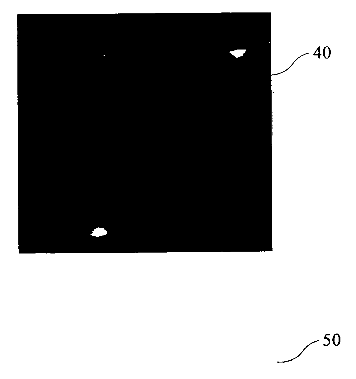
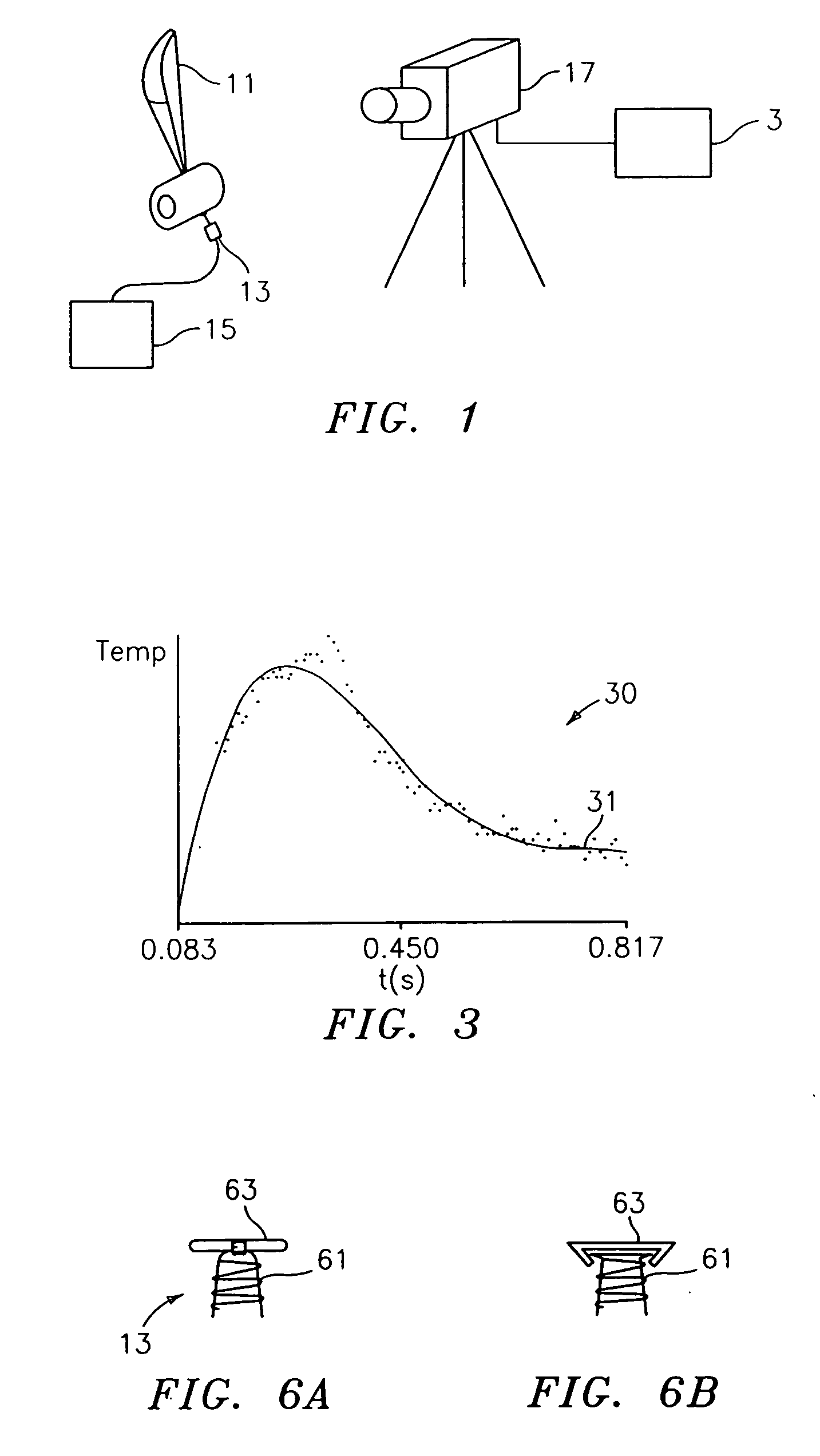
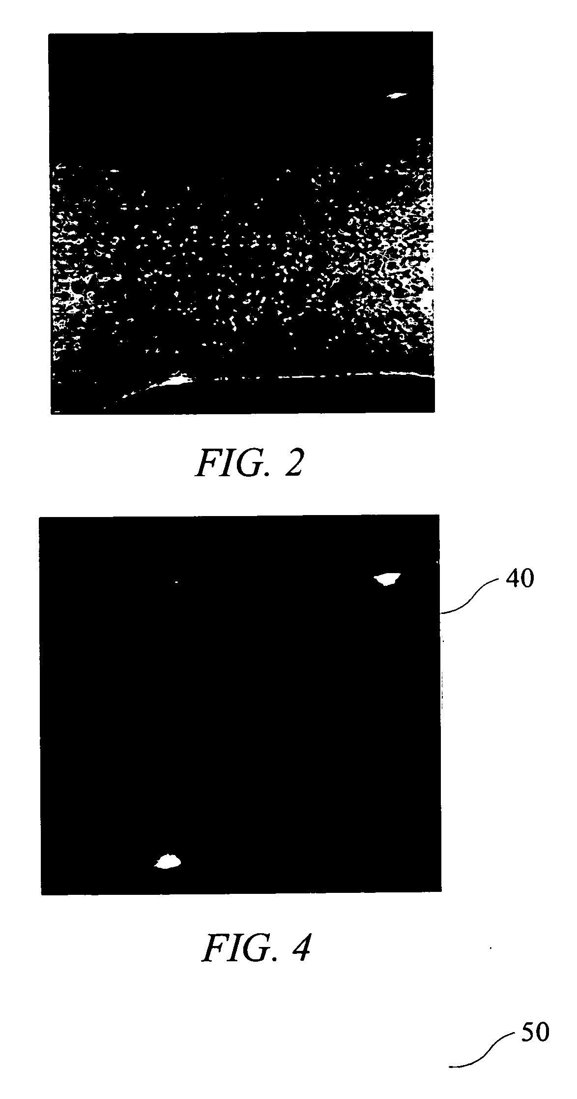
- A method and apparatus utilizing broad-band acoustic energy to induce mechanical energy in structures, combined with infrared imaging to capture and process images of emitted energy, enabling more comprehensive defect detection by employing a broad-spectrum acoustic signal and real-time image processing.

Apparatus and method for inspecting microstructures in reflected or transmitted infrared light
PatentInactiveEP1756645A1
Innovation
- A device and method that enables simultaneous or separate incident and transmitted light illumination in the IR range, combined with visual incident light, using a microscope with interchangeable filters and switchable diaphragms, allowing for high-contrast imaging of microstructured samples, including those with metallization layers, by utilizing IR lenses and an autofocus system for automation.
Semiconductor Manufacturing Quality Standards Impact
The implementation of void detection technologies in wafer bonding processes has fundamentally transformed semiconductor manufacturing quality standards, establishing new benchmarks for defect identification and process control. Both infrared (IR) imaging and acoustic microscopy have become integral components of quality assurance frameworks, driving the evolution of inspection protocols from traditional visual methods to sophisticated non-destructive testing approaches.
Current quality standards in semiconductor manufacturing, particularly those governed by JEDEC, SEMI, and ISO specifications, now explicitly incorporate void detection requirements for bonded wafer structures. These standards mandate maximum allowable void sizes, typically ranging from 10-50 micrometers depending on the application, and establish minimum detection sensitivity requirements that directly influence the selection between IR and acoustic imaging technologies.
The integration of advanced void detection methods has led to the establishment of statistical process control (SPC) parameters specifically designed for bonded wafer quality assessment. Manufacturing facilities now implement real-time monitoring systems that utilize both IR and acoustic data to maintain process stability and ensure compliance with increasingly stringent quality metrics. This dual-technology approach has become essential for meeting automotive and aerospace semiconductor reliability standards.
Quality certification processes have adapted to accommodate the unique capabilities of each detection method. IR imaging systems are now standardized for rapid, high-throughput screening applications, while acoustic microscopy has become the reference standard for critical applications requiring sub-surface defect characterization. This differentiation has resulted in tiered quality control strategies that optimize inspection efficiency while maintaining detection accuracy.
The impact extends to supplier qualification requirements, where semiconductor manufacturers now mandate specific void detection capabilities from their equipment vendors. This has accelerated the development of hybrid inspection systems that combine both technologies, enabling comprehensive quality assessment that meets the most demanding industry standards while supporting continuous improvement initiatives in wafer bonding processes.
Current quality standards in semiconductor manufacturing, particularly those governed by JEDEC, SEMI, and ISO specifications, now explicitly incorporate void detection requirements for bonded wafer structures. These standards mandate maximum allowable void sizes, typically ranging from 10-50 micrometers depending on the application, and establish minimum detection sensitivity requirements that directly influence the selection between IR and acoustic imaging technologies.
The integration of advanced void detection methods has led to the establishment of statistical process control (SPC) parameters specifically designed for bonded wafer quality assessment. Manufacturing facilities now implement real-time monitoring systems that utilize both IR and acoustic data to maintain process stability and ensure compliance with increasingly stringent quality metrics. This dual-technology approach has become essential for meeting automotive and aerospace semiconductor reliability standards.
Quality certification processes have adapted to accommodate the unique capabilities of each detection method. IR imaging systems are now standardized for rapid, high-throughput screening applications, while acoustic microscopy has become the reference standard for critical applications requiring sub-surface defect characterization. This differentiation has resulted in tiered quality control strategies that optimize inspection efficiency while maintaining detection accuracy.
The impact extends to supplier qualification requirements, where semiconductor manufacturers now mandate specific void detection capabilities from their equipment vendors. This has accelerated the development of hybrid inspection systems that combine both technologies, enabling comprehensive quality assessment that meets the most demanding industry standards while supporting continuous improvement initiatives in wafer bonding processes.
Cost-Benefit Analysis of Detection Method Implementation
The implementation of void detection methods in wafer bonding processes requires careful evaluation of capital expenditure, operational costs, and return on investment. Infrared imaging systems typically demand lower initial capital investment compared to acoustic imaging equipment, with basic IR systems ranging from $50,000 to $200,000 depending on resolution and automation capabilities. Advanced acoustic imaging systems generally require higher upfront costs, often exceeding $300,000 for comprehensive solutions with high-frequency transducers and sophisticated signal processing capabilities.
Operational expenditure analysis reveals distinct cost structures for each method. IR imaging systems demonstrate lower maintenance requirements due to fewer moving components and solid-state detector technology, resulting in annual maintenance costs typically below 5% of initial investment. Training requirements are minimal as IR imaging provides intuitive visual output that operators can readily interpret. Conversely, acoustic imaging systems require specialized technical expertise for operation and maintenance, with annual service costs often reaching 8-12% of capital investment due to complex transducer calibration and signal processing requirements.
Throughput considerations significantly impact cost-effectiveness calculations. IR imaging enables rapid full-wafer scanning within seconds, supporting high-volume production environments without creating bottlenecks. This speed advantage translates to lower cost-per-inspection ratios in mass production scenarios. Acoustic imaging, while slower due to mechanical scanning requirements, offers superior detection sensitivity that can prevent costly downstream failures, particularly valuable in high-reliability applications where defect escape costs are substantial.
The total cost of ownership analysis must incorporate detection accuracy impacts on yield and quality metrics. IR imaging's limitation in detecting smaller voids may result in higher defect escape rates, potentially leading to increased warranty costs and customer returns. Acoustic imaging's superior sensitivity to sub-micron voids provides enhanced quality assurance, justifying higher implementation costs through reduced field failure rates and improved customer satisfaction metrics.
Return on investment calculations favor different methods depending on application requirements. High-volume consumer electronics manufacturing typically benefits from IR imaging's speed and lower operational costs, achieving payback periods of 12-18 months. Critical applications in aerospace or medical devices often justify acoustic imaging investments through quality premium pricing and reduced liability exposure, despite longer payback periods of 24-36 months.
Operational expenditure analysis reveals distinct cost structures for each method. IR imaging systems demonstrate lower maintenance requirements due to fewer moving components and solid-state detector technology, resulting in annual maintenance costs typically below 5% of initial investment. Training requirements are minimal as IR imaging provides intuitive visual output that operators can readily interpret. Conversely, acoustic imaging systems require specialized technical expertise for operation and maintenance, with annual service costs often reaching 8-12% of capital investment due to complex transducer calibration and signal processing requirements.
Throughput considerations significantly impact cost-effectiveness calculations. IR imaging enables rapid full-wafer scanning within seconds, supporting high-volume production environments without creating bottlenecks. This speed advantage translates to lower cost-per-inspection ratios in mass production scenarios. Acoustic imaging, while slower due to mechanical scanning requirements, offers superior detection sensitivity that can prevent costly downstream failures, particularly valuable in high-reliability applications where defect escape costs are substantial.
The total cost of ownership analysis must incorporate detection accuracy impacts on yield and quality metrics. IR imaging's limitation in detecting smaller voids may result in higher defect escape rates, potentially leading to increased warranty costs and customer returns. Acoustic imaging's superior sensitivity to sub-micron voids provides enhanced quality assurance, justifying higher implementation costs through reduced field failure rates and improved customer satisfaction metrics.
Return on investment calculations favor different methods depending on application requirements. High-volume consumer electronics manufacturing typically benefits from IR imaging's speed and lower operational costs, achieving payback periods of 12-18 months. Critical applications in aerospace or medical devices often justify acoustic imaging investments through quality premium pricing and reduced liability exposure, despite longer payback periods of 24-36 months.
Unlock deeper insights with PatSnap Eureka Quick Research — get a full tech report to explore trends and direct your research. Try now!
Generate Your Research Report Instantly with AI Agent
Supercharge your innovation with PatSnap Eureka AI Agent Platform!