Controlling Layer Thickness In Multilayer PVD Coatings
APR 8, 20269 MIN READ
Generate Your Research Report Instantly with AI Agent
PatSnap Eureka helps you evaluate technical feasibility & market potential.
PVD Multilayer Coating Technology Background and Objectives
Physical Vapor Deposition (PVD) multilayer coating technology has emerged as a critical surface engineering solution since its commercial introduction in the 1960s. Initially developed for decorative applications, PVD has evolved into a sophisticated manufacturing process capable of producing complex multilayer structures with nanometer-scale precision. The technology's foundation lies in the controlled deposition of thin films through physical processes such as sputtering, evaporation, and ion plating, enabling the creation of coatings with tailored properties that cannot be achieved through single-layer approaches.
The evolution of PVD multilayer coatings has been driven by increasing demands for enhanced performance in extreme operating conditions. Modern applications require coatings that simultaneously exhibit superior hardness, wear resistance, thermal stability, and corrosion protection. Traditional monolithic coatings often fail to meet these multifaceted requirements, leading to the development of multilayer architectures where individual layers contribute specific functionalities while working synergistically to achieve overall performance objectives.
Contemporary multilayer PVD systems typically consist of alternating layers with thicknesses ranging from several nanometers to micrometers. The precise control of individual layer thickness has become paramount, as even minor deviations can significantly impact coating performance. Research has demonstrated that optimal layer thickness ratios can enhance hardness through Hall-Petch strengthening mechanisms, improve thermal barrier properties through phonon scattering, and increase fracture toughness through crack deflection and energy dissipation mechanisms.
The primary objective of advanced multilayer PVD coating technology centers on achieving unprecedented control over layer thickness uniformity and repeatability. This involves developing real-time monitoring systems, advanced process control algorithms, and predictive models that can maintain thickness variations within ±2% across large substrate areas. Secondary objectives include optimizing interface quality, minimizing residual stress gradients, and establishing scalable manufacturing processes suitable for high-volume production environments.
Current technological goals also encompass the integration of artificial intelligence and machine learning algorithms to predict optimal layer thickness combinations for specific applications. This includes developing adaptive control systems that can automatically adjust deposition parameters based on real-time feedback, ensuring consistent coating quality while minimizing material waste and production time.
Market Demand for Precision Multilayer PVD Coatings
The global market for precision multilayer PVD coatings has experienced substantial growth driven by increasing demands across multiple high-technology sectors. The semiconductor industry represents the largest market segment, where precise layer thickness control is critical for manufacturing advanced microprocessors, memory devices, and photonic components. As semiconductor nodes continue to shrink and device architectures become more complex, the requirements for atomic-level precision in multilayer coating deposition have intensified significantly.
Optical applications constitute another major market driver, particularly in the production of high-performance optical filters, anti-reflective coatings, and beam splitters used in telecommunications, laser systems, and advanced imaging equipment. The growing deployment of fiber optic networks and the expansion of photonics-based technologies have created sustained demand for multilayer optical coatings with precisely controlled thickness gradients and interface properties.
The aerospace and defense sectors have emerged as significant consumers of precision multilayer PVD coatings, utilizing these technologies for thermal barrier coatings on turbine components, stealth applications, and satellite instrumentation. The stringent performance requirements in these applications necessitate exceptional control over individual layer thicknesses to achieve desired thermal, mechanical, and electromagnetic properties.
Medical device manufacturing has shown increasing adoption of precision multilayer coatings for biocompatible implants, surgical instruments, and diagnostic equipment. The ability to control layer thickness at nanometer scales enables the creation of surfaces with tailored biocompatibility, wear resistance, and antimicrobial properties.
Market growth is further supported by the automotive industry's transition toward electric vehicles and advanced driver assistance systems, which require sophisticated sensor coatings and electronic components with precisely controlled multilayer structures. The renewable energy sector, particularly solar panel manufacturing, also contributes to market expansion through demand for optimized anti-reflective and selective absorber coatings.
Regional market dynamics show strong growth in Asia-Pacific regions, driven by semiconductor manufacturing concentration and expanding electronics production capabilities. North American and European markets maintain significant demand through aerospace, defense, and advanced manufacturing applications, emphasizing the global nature of precision multilayer PVD coating requirements.
Current State and Challenges in Layer Thickness Control
The current state of layer thickness control in multilayer PVD coatings represents a complex technological landscape where precision requirements continue to escalate while manufacturing constraints persist. Modern industrial applications demand thickness tolerances at the nanometer scale, with some advanced optical and electronic applications requiring variations of less than ±1% across entire substrate surfaces. This level of precision pushes existing control methodologies to their operational limits.
Real-time monitoring capabilities have emerged as a critical bottleneck in achieving consistent layer thickness control. Traditional quartz crystal microbalance systems, while widely adopted, suffer from drift issues and limited spatial resolution across large substrates. Optical monitoring techniques, including ellipsometry and reflectometry, provide superior accuracy but face challenges in multilayer systems where interference effects from multiple interfaces can obscure individual layer measurements.
Process parameter stability remains a fundamental challenge affecting thickness uniformity. Variations in target erosion patterns, chamber geometry effects, and substrate positioning create systematic thickness gradients that are difficult to compensate. Power delivery fluctuations, particularly in reactive sputtering processes, introduce additional complexity as they affect both deposition rate and film stoichiometry simultaneously.
The integration of multiple deposition sources in multilayer systems compounds control difficulties. Cross-contamination between adjacent layers, thermal effects from sequential depositions, and the need for precise timing coordination between different sputtering targets create interdependent variables that are challenging to optimize simultaneously. Chamber design limitations often force compromises between throughput and uniformity.
Advanced control algorithms incorporating machine learning approaches show promise but face implementation barriers. The high-dimensional parameter space, coupled with limited real-time feedback mechanisms, makes it difficult to establish robust process models. Additionally, the proprietary nature of many industrial PVD systems limits the integration of sophisticated control strategies.
Substrate-related factors introduce another layer of complexity, particularly for large-area or three-dimensional substrates. Temperature gradients, surface roughness variations, and geometric shadowing effects create position-dependent deposition conditions that require sophisticated compensation strategies. The challenge intensifies when processing temperature-sensitive substrates that limit process parameter flexibility.
Existing Solutions for Multilayer Thickness Control
01 Optimization of individual layer thickness in multilayer PVD coatings
Multilayer PVD coatings can be optimized by controlling the thickness of individual layers to achieve desired properties such as wear resistance, hardness, and thermal stability. The thickness of each layer can be precisely controlled during the deposition process, typically ranging from nanometers to micrometers. By adjusting the thickness of individual layers, the overall performance of the coating system can be enhanced, including improved adhesion between layers and reduced internal stress.- Optimization of individual layer thickness in multilayer PVD coatings: Multilayer PVD coatings can be optimized by controlling the thickness of individual layers to achieve desired properties such as wear resistance, hardness, and adhesion. The thickness of each layer can be precisely controlled during the deposition process, typically ranging from nanometers to micrometers. Proper layer thickness optimization helps in achieving uniform coating properties and preventing delamination or cracking.
- Alternating layer structure with varying thickness ratios: Multilayer PVD coatings can be designed with alternating layers of different materials where the thickness ratio between adjacent layers is carefully controlled. This approach allows for the creation of superlattice structures or nanolayered coatings that exhibit enhanced mechanical properties. The thickness ratio between different material layers can be adjusted to optimize stress distribution and improve coating performance.
- Gradient layer thickness design in multilayer coatings: Gradient multilayer PVD coatings feature layers with progressively varying thickness from the substrate to the surface. This design helps in managing residual stress, improving adhesion to the substrate, and providing a smooth transition in properties. The gradient approach can involve either continuously changing layer thickness or stepwise thickness variations throughout the coating structure.
- Measurement and control methods for layer thickness: Various techniques are employed to measure and control layer thickness during multilayer PVD coating deposition. These methods include in-situ monitoring systems, optical measurement techniques, and process parameter control. Accurate thickness control is essential for maintaining coating quality and reproducibility. Advanced monitoring systems enable real-time adjustment of deposition parameters to achieve target layer thicknesses.
- Total coating thickness and layer number relationship: The relationship between total coating thickness and the number of individual layers in multilayer PVD coatings is critical for achieving optimal performance. Increasing the number of layers while maintaining a constant total thickness results in thinner individual layers, which can enhance certain properties such as toughness and crack resistance. The selection of appropriate layer numbers and individual layer thicknesses depends on the intended application and required coating characteristics.
02 Nanoscale multilayer architecture with alternating thin layers
Nanoscale multilayer PVD coatings feature alternating thin layers with thicknesses in the nanometer range. This architecture creates interfaces that can impede crack propagation and enhance mechanical properties. The periodicity and thickness of these nanolayers are critical parameters that influence the coating's hardness, toughness, and resistance to deformation. Such structures can be designed with layer thicknesses ranging from a few nanometers to several tens of nanometers.Expand Specific Solutions03 Gradient layer thickness distribution in multilayer coatings
Gradient multilayer PVD coatings employ a systematic variation in layer thickness throughout the coating structure. This approach allows for a gradual transition in properties from the substrate to the surface, which can reduce stress concentrations and improve adhesion. The thickness gradient can be designed to optimize specific performance characteristics, with layers progressively increasing or decreasing in thickness according to functional requirements.Expand Specific Solutions04 Total coating thickness control in multilayer PVD systems
The total thickness of multilayer PVD coatings is a critical parameter that affects the overall performance and durability of the coating system. Total thickness typically ranges from a few micrometers to several tens of micrometers, depending on the application requirements. Controlling the total thickness while maintaining the integrity of individual layers is essential for achieving optimal mechanical properties, wear resistance, and coating longevity. Precise thickness control is achieved through monitoring deposition rates and time.Expand Specific Solutions05 Measurement and characterization techniques for layer thickness
Various measurement and characterization techniques are employed to determine and verify the thickness of individual layers and total coating thickness in multilayer PVD systems. These techniques include cross-sectional microscopy, profilometry, and non-destructive methods. Accurate thickness measurement is essential for quality control and ensuring that the coating meets specified requirements. Advanced characterization methods can provide detailed information about layer uniformity, interface quality, and thickness distribution across the coated surface.Expand Specific Solutions
Key Players in PVD Equipment and Coating Industry
The multilayer PVD coating layer thickness control technology represents a mature industrial sector experiencing steady growth, driven by increasing demand across automotive, aerospace, and semiconductor applications. The global PVD coating market, valued at approximately $25 billion, demonstrates robust expansion as industries seek enhanced surface properties and performance optimization. Technology maturity varies significantly among key players, with established leaders like Applied Materials, Lam Research, and SPTS Technologies driving semiconductor equipment innovation, while Oerlikon Surface Solutions and companies like Kennametal, Walter AG, and SECO Tools advance industrial tooling applications. Traditional manufacturers such as Sumitomo Electric Industries and Robert Bosch leverage extensive R&D capabilities for automotive components, whereas specialized firms like Carl Zeiss SMT focus on precision optics. The competitive landscape reflects a consolidating market where technological differentiation centers on precision control algorithms, real-time monitoring systems, and process repeatability, with emerging players from Asia challenging established Western dominance through cost-effective solutions and rapid technological adoption.
Oerlikon Surface Solutions AG
Technical Solution: Oerlikon has developed advanced PVD coating systems with precise layer thickness control through real-time monitoring and feedback systems. Their technology utilizes magnetron sputtering with closed-loop control algorithms that monitor deposition rates and adjust process parameters dynamically. The company's ePD (enhanced Physical Deposition) technology enables nanometer-level precision in multilayer coating thickness control, incorporating advanced plasma diagnostics and substrate temperature management. Their systems feature multiple cathode configurations and sophisticated power supply control to ensure uniform layer distribution across large substrate areas.
Strengths: Industry-leading precision control, comprehensive process monitoring capabilities, scalable industrial solutions. Weaknesses: High capital investment requirements, complex system maintenance needs.
SPTS Technologies Ltd.
Technical Solution: SPTS Technologies specializes in PVD systems with advanced layer thickness control for MEMS and semiconductor applications. Their Sigma series PVD systems incorporate proprietary thickness monitoring technology using optical interferometry and real-time process feedback control. The company's approach features multi-target configurations with independent power control for each source, enabling precise multilayer deposition with nanometer-level accuracy. Their systems include advanced substrate heating and cooling capabilities, along with sophisticated process recipe management software that automatically adjusts deposition parameters to maintain target layer thicknesses throughout the coating process.
Strengths: Specialized MEMS expertise, precise optical monitoring systems, flexible multi-target configurations. Weaknesses: Smaller market presence compared to major competitors, limited to specialized applications.
Core Innovations in Real-time PVD Process Monitoring
Method for producing a dielectric and/or barrier layer or multilayer on a substrate, and device for implementing said method
PatentInactiveUS20150325418A1
Innovation
- A combined process using Plasma Enhanced Chemical Vapor Deposition (PECVD) and Physical Vapor Deposition (PVD) techniques to create dielectric and barrier layers, allowing for simultaneous deposition in a single vacuum chamber with independent control of plasma sources, enhancing conformality, thickness, and mechanical stability, and optimizing dielectric breakdown properties.

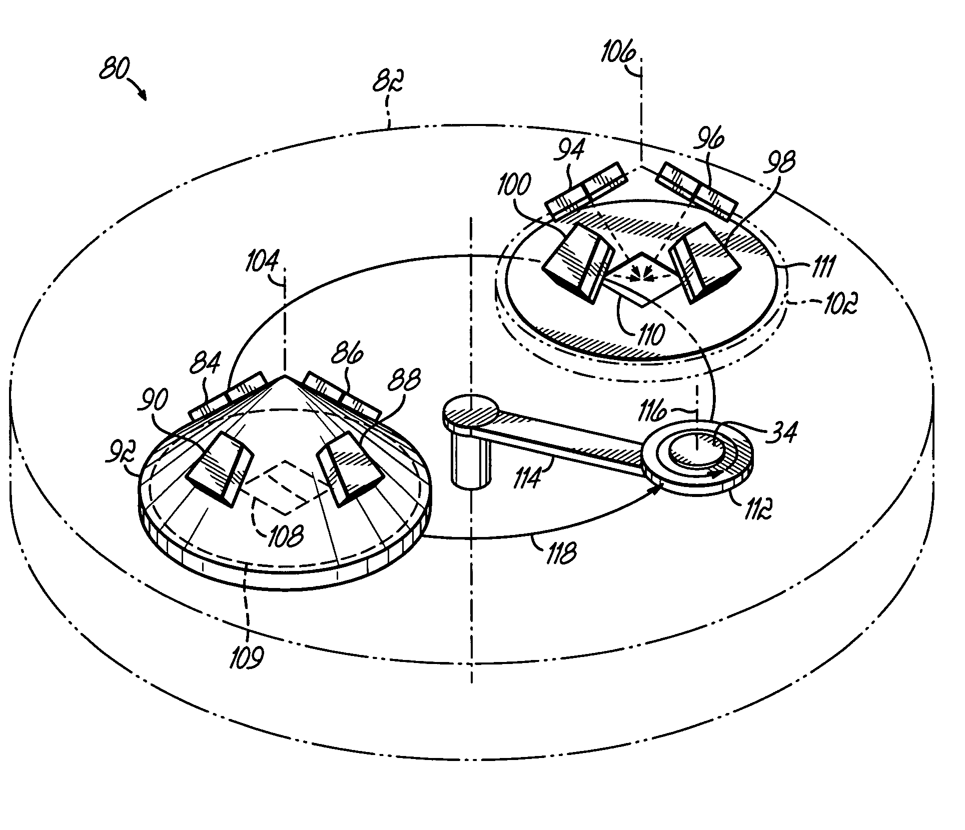
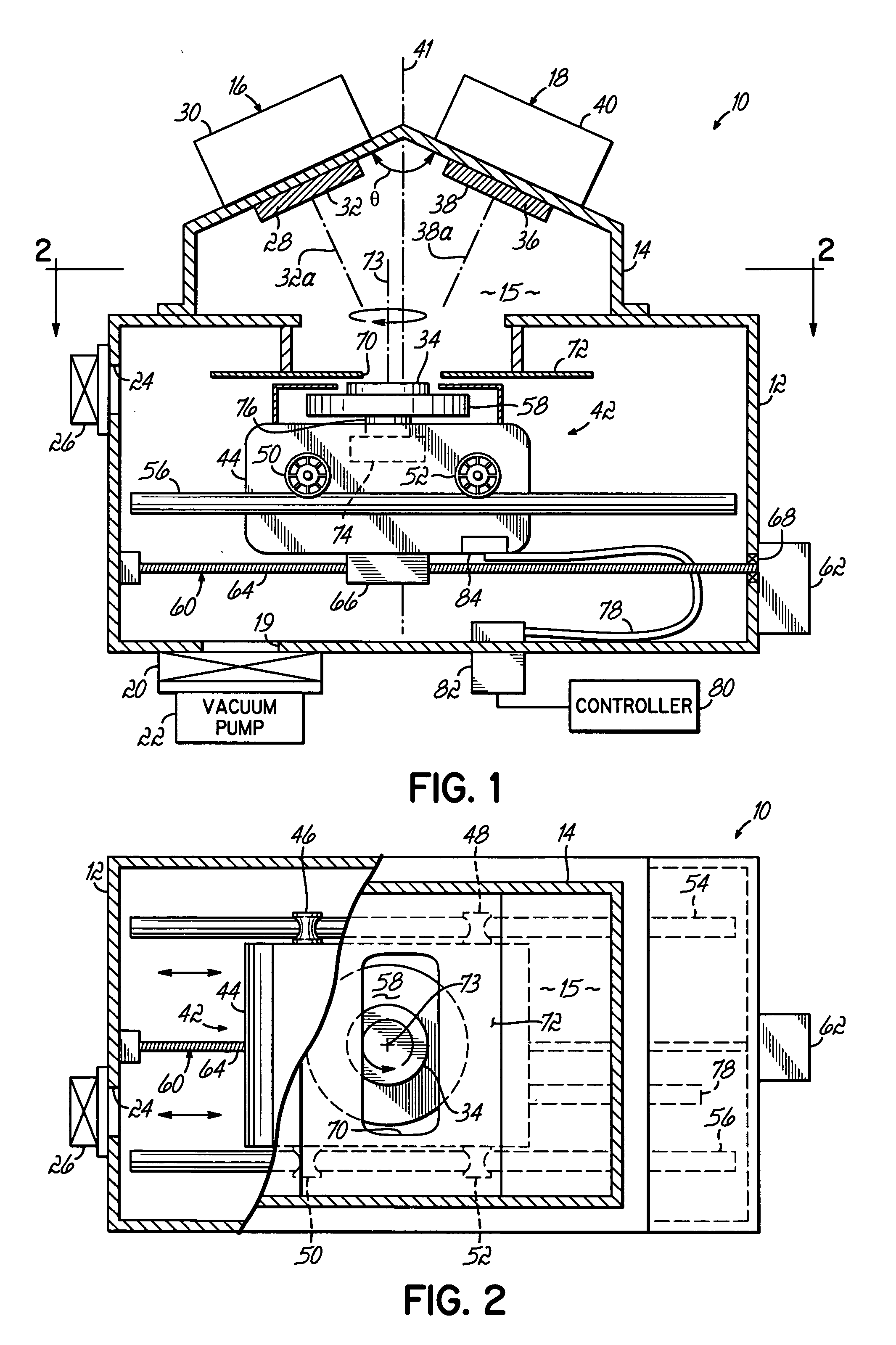
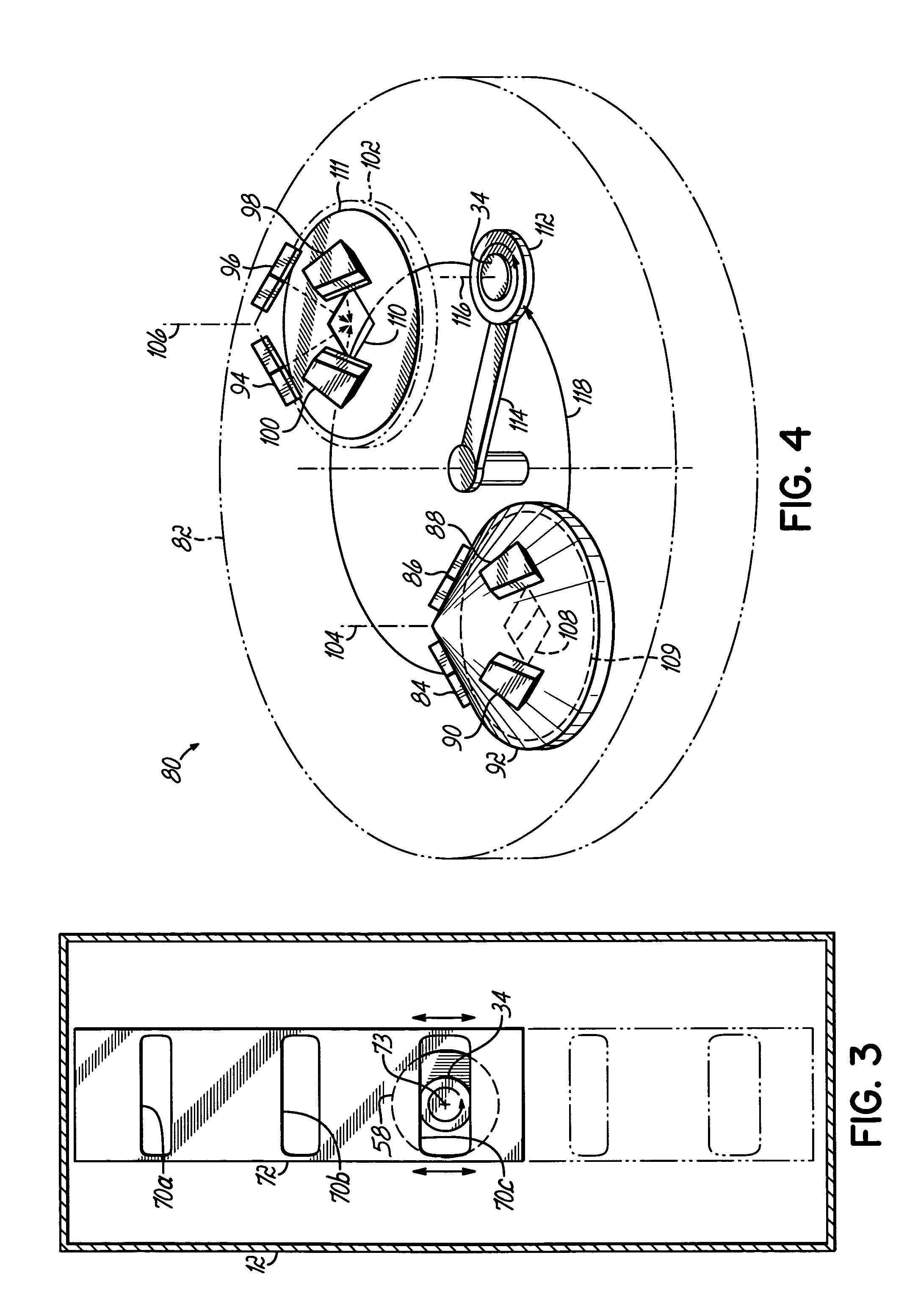
Physical vapor deposition apparatus for depositing thin multilayer films and methods of depositing such films
PatentInactiveUS20060054494A1
Innovation
- A compact PVD module with a conical cluster of confocally arranged sputter sources and a substrate carrier that rotates and translates through a defined deposition zone, eliminating the need for shutters and achieving precise control of film thickness, uniformity, and smoothness using independent substrate motions.
Quality Standards for Industrial PVD Applications
Quality standards for industrial PVD applications represent a critical framework that ensures consistent performance and reliability in multilayer coating systems. These standards encompass dimensional accuracy, surface quality, adhesion strength, and coating uniformity requirements that directly impact the effectiveness of layer thickness control strategies. International standards such as ISO 4516, ASTM B733, and DIN EN 1071 provide comprehensive guidelines for coating thickness measurement, surface preparation, and quality assessment protocols.
Thickness tolerance specifications form the cornerstone of PVD quality standards, typically requiring layer thickness variations within ±5% for critical applications such as aerospace components and precision tooling. Advanced industrial applications often demand even tighter tolerances, with some semiconductor and optical coating applications requiring thickness control within ±1-2%. These stringent requirements necessitate sophisticated monitoring systems and real-time feedback mechanisms during the deposition process.
Surface roughness and morphology standards play a crucial role in multilayer PVD coating quality assessment. Ra values typically range from 0.1 to 0.5 micrometers for most industrial applications, while specialized optical coatings may require surface roughness below 0.05 micrometers. The standards also define acceptable defect densities, including pinholes, particles, and coating discontinuities that could compromise layer integrity and performance.
Adhesion strength requirements constitute another fundamental aspect of quality standards, with typical specifications ranging from 20-60 N for critical load-bearing applications. Standardized testing methods such as scratch testing, pull-off testing, and thermal cycling evaluations ensure that multilayer coatings maintain structural integrity under operational conditions. These tests are particularly important for multilayer systems where interlayer adhesion can significantly impact overall coating performance.
Chemical composition and purity standards define acceptable levels of contamination and elemental distribution within individual layers. X-ray photoelectron spectroscopy and secondary ion mass spectrometry are commonly employed to verify compliance with compositional requirements, ensuring that each layer maintains its intended properties and functionality within the multilayer architecture.
Environmental testing standards simulate real-world operating conditions through accelerated aging, corrosion resistance, and thermal stability assessments. These standards typically require coatings to withstand temperature cycling between -40°C to 200°C, humidity exposure up to 95% relative humidity, and salt spray testing for corrosion resistance evaluation, ensuring long-term performance reliability in diverse industrial environments.
Cost-Performance Analysis of Advanced PVD Systems
The economic evaluation of advanced PVD systems for multilayer coating applications reveals significant variations in cost-performance ratios across different technological approaches. Traditional magnetron sputtering systems typically require initial capital investments ranging from $200,000 to $800,000, while advanced ion beam assisted deposition (IBAD) systems can exceed $1.5 million. However, the superior layer thickness control capabilities of premium systems often justify higher upfront costs through improved yield rates and reduced material waste.
Operational expenses constitute a substantial portion of total ownership costs, with energy consumption being a primary factor. Advanced systems incorporating closed-loop thickness monitoring demonstrate 15-25% lower operational costs compared to conventional open-loop systems. The integration of real-time ellipsometry and quartz crystal microbalance sensors, while adding $50,000-$100,000 to system costs, typically reduces material consumption by 8-12% and increases process repeatability by over 30%.
Throughput analysis indicates that high-end systems with automated substrate handling and multi-chamber configurations achieve 40-60% higher productivity rates. These systems process 200-300 substrates per day compared to 120-180 for standard configurations. The enhanced throughput directly impacts per-unit coating costs, reducing them from $15-25 to $8-15 for typical optical multilayer applications.
Return on investment calculations demonstrate that advanced PVD systems with precise thickness control capabilities typically achieve payback periods of 18-24 months in high-volume production environments. The reduced rejection rates, improved coating uniformity, and enhanced process stability contribute to overall cost savings of 20-35% over three-year operational periods.
Maintenance and consumable costs vary significantly between system types. Advanced systems with predictive maintenance capabilities and automated component replacement reduce downtime by 25-40%, translating to annual savings of $80,000-$150,000 for continuous production facilities. Target utilization efficiency improvements of 15-20% further enhance the economic attractiveness of premium PVD systems for precision multilayer coating applications.
Unlock deeper insights with PatSnap Eureka Quick Research — get a full tech report to explore trends and direct your research. Try now!
Generate Your Research Report Instantly with AI Agent
Supercharge your innovation with PatSnap Eureka AI Agent Platform!