
Copper Clip Bonding vs Wire Mesh Layers: Signal Reflection Differences
MAY 22, 20269 MIN READ
Generate Your Research Report Instantly with AI Agent
Patsnap Eureka helps you evaluate technical feasibility & market potential.
Copper Interconnect Technology Background and Objectives
Copper interconnect technology has emerged as the cornerstone of modern semiconductor packaging and electronic system integration, fundamentally transforming how electrical connections are established within integrated circuits and multi-chip modules. The evolution from aluminum-based interconnects to copper-based solutions marked a pivotal transition in the semiconductor industry, driven by the relentless pursuit of higher performance, reduced power consumption, and enhanced reliability in increasingly miniaturized electronic devices.
The historical development of copper interconnect technology traces back to the late 1990s when the semiconductor industry recognized the limitations of traditional aluminum metallization in meeting the demands of sub-micron technology nodes. Copper's superior electrical conductivity, approximately 40% better than aluminum, coupled with its improved electromigration resistance, positioned it as the ideal candidate for next-generation interconnect systems. This transition catalyzed the development of various copper interconnect methodologies, including wire bonding, clip bonding, and advanced packaging techniques.
Within the broader copper interconnect landscape, two distinct approaches have gained significant attention: copper clip bonding and wire mesh layer configurations. These methodologies represent different philosophical approaches to achieving optimal electrical performance while addressing the inherent challenges of signal integrity in high-frequency applications. The fundamental distinction lies in their geometric configurations and the resulting electromagnetic field distributions, which directly influence signal propagation characteristics and reflection behaviors.
The primary objective of investigating copper clip bonding versus wire mesh layers centers on understanding and quantifying the signal reflection differences between these two interconnect approaches. Signal reflection, a critical parameter in high-speed digital and RF applications, directly impacts system performance, power efficiency, and electromagnetic compatibility. The geometric and material properties of each interconnect method create distinct impedance profiles and electromagnetic field patterns, leading to measurably different reflection coefficients across various frequency ranges.
Current technological objectives focus on developing comprehensive models and experimental methodologies to characterize the reflection behavior of both copper clip bonding and wire mesh layer implementations. This includes establishing standardized measurement protocols, developing predictive simulation frameworks, and identifying optimal design parameters for specific application requirements. The ultimate goal involves creating design guidelines that enable engineers to select the most appropriate copper interconnect technology based on performance specifications, manufacturing constraints, and cost considerations.
The strategic importance of this research extends beyond immediate technical benefits, encompassing long-term implications for next-generation electronic systems including 5G communications, automotive electronics, and high-performance computing platforms where signal integrity requirements continue to escalate with increasing operational frequencies and data rates.
The historical development of copper interconnect technology traces back to the late 1990s when the semiconductor industry recognized the limitations of traditional aluminum metallization in meeting the demands of sub-micron technology nodes. Copper's superior electrical conductivity, approximately 40% better than aluminum, coupled with its improved electromigration resistance, positioned it as the ideal candidate for next-generation interconnect systems. This transition catalyzed the development of various copper interconnect methodologies, including wire bonding, clip bonding, and advanced packaging techniques.
Within the broader copper interconnect landscape, two distinct approaches have gained significant attention: copper clip bonding and wire mesh layer configurations. These methodologies represent different philosophical approaches to achieving optimal electrical performance while addressing the inherent challenges of signal integrity in high-frequency applications. The fundamental distinction lies in their geometric configurations and the resulting electromagnetic field distributions, which directly influence signal propagation characteristics and reflection behaviors.
The primary objective of investigating copper clip bonding versus wire mesh layers centers on understanding and quantifying the signal reflection differences between these two interconnect approaches. Signal reflection, a critical parameter in high-speed digital and RF applications, directly impacts system performance, power efficiency, and electromagnetic compatibility. The geometric and material properties of each interconnect method create distinct impedance profiles and electromagnetic field patterns, leading to measurably different reflection coefficients across various frequency ranges.
Current technological objectives focus on developing comprehensive models and experimental methodologies to characterize the reflection behavior of both copper clip bonding and wire mesh layer implementations. This includes establishing standardized measurement protocols, developing predictive simulation frameworks, and identifying optimal design parameters for specific application requirements. The ultimate goal involves creating design guidelines that enable engineers to select the most appropriate copper interconnect technology based on performance specifications, manufacturing constraints, and cost considerations.
The strategic importance of this research extends beyond immediate technical benefits, encompassing long-term implications for next-generation electronic systems including 5G communications, automotive electronics, and high-performance computing platforms where signal integrity requirements continue to escalate with increasing operational frequencies and data rates.
Market Demand for Advanced PCB Signal Integrity Solutions
The global electronics industry is experiencing unprecedented demand for high-performance printed circuit boards that can maintain signal integrity at increasingly higher frequencies. As electronic devices become more compact and operate at faster speeds, the need for advanced PCB solutions that minimize signal reflection has become critical across multiple market segments.
Consumer electronics manufacturers are driving significant demand for improved signal integrity solutions as they develop next-generation smartphones, tablets, and wearable devices. These products require PCBs that can handle high-frequency signals while maintaining compact form factors. The proliferation of 5G technology has intensified this demand, as devices must support higher data rates and more complex signal processing requirements.
The automotive sector represents another major growth driver for advanced PCB signal integrity solutions. Modern vehicles incorporate numerous electronic control units, advanced driver assistance systems, and infotainment platforms that rely on high-speed digital communications. Electric vehicles and autonomous driving technologies further amplify the need for reliable signal transmission in harsh operating environments.
Data center and telecommunications infrastructure markets are experiencing robust growth in demand for PCBs with superior signal integrity characteristics. Cloud computing expansion, edge computing deployment, and the rollout of 5G networks require high-performance server boards and networking equipment that can handle massive data throughput with minimal signal degradation.
Industrial automation and Internet of Things applications are creating new market opportunities for specialized PCB solutions. Manufacturing equipment, robotics, and sensor networks require reliable signal transmission in challenging industrial environments where electromagnetic interference and temperature variations can affect performance.
The aerospace and defense sectors maintain consistent demand for high-reliability PCB solutions with exceptional signal integrity performance. Military communications systems, radar equipment, and satellite technology require PCBs that can operate reliably under extreme conditions while maintaining precise signal characteristics.
Market research indicates that signal integrity challenges are becoming more complex as operating frequencies continue to increase across all application domains. Traditional PCB design approaches are reaching their limits, creating opportunities for innovative solutions that address specific signal reflection issues through advanced materials, novel interconnection methods, and optimized layer stack-up designs.
Consumer electronics manufacturers are driving significant demand for improved signal integrity solutions as they develop next-generation smartphones, tablets, and wearable devices. These products require PCBs that can handle high-frequency signals while maintaining compact form factors. The proliferation of 5G technology has intensified this demand, as devices must support higher data rates and more complex signal processing requirements.
The automotive sector represents another major growth driver for advanced PCB signal integrity solutions. Modern vehicles incorporate numerous electronic control units, advanced driver assistance systems, and infotainment platforms that rely on high-speed digital communications. Electric vehicles and autonomous driving technologies further amplify the need for reliable signal transmission in harsh operating environments.
Data center and telecommunications infrastructure markets are experiencing robust growth in demand for PCBs with superior signal integrity characteristics. Cloud computing expansion, edge computing deployment, and the rollout of 5G networks require high-performance server boards and networking equipment that can handle massive data throughput with minimal signal degradation.
Industrial automation and Internet of Things applications are creating new market opportunities for specialized PCB solutions. Manufacturing equipment, robotics, and sensor networks require reliable signal transmission in challenging industrial environments where electromagnetic interference and temperature variations can affect performance.
The aerospace and defense sectors maintain consistent demand for high-reliability PCB solutions with exceptional signal integrity performance. Military communications systems, radar equipment, and satellite technology require PCBs that can operate reliably under extreme conditions while maintaining precise signal characteristics.
Market research indicates that signal integrity challenges are becoming more complex as operating frequencies continue to increase across all application domains. Traditional PCB design approaches are reaching their limits, creating opportunities for innovative solutions that address specific signal reflection issues through advanced materials, novel interconnection methods, and optimized layer stack-up designs.
Current Challenges in Copper Bonding Signal Reflection Control
The control of signal reflection in copper bonding applications faces significant technical barriers that directly impact the performance comparison between copper clip bonding and wire mesh layer configurations. Impedance matching represents the most critical challenge, as the abrupt transition from semiconductor die to copper interconnects creates substantial reflection coefficients that can exceed acceptable thresholds for high-frequency applications.
Geometric discontinuities pose another fundamental obstacle in copper bonding signal reflection control. The three-dimensional nature of copper clip connections introduces complex field distributions that are difficult to predict and optimize. Unlike traditional wire bonding where the signal path follows a predictable arc, copper clips create multiple reflection points due to their rectangular cross-sections and varying contact geometries with both die pads and substrate lands.
Frequency-dependent losses become increasingly problematic as operating frequencies extend beyond 10 GHz. The skin effect in copper conductors, combined with dielectric losses in surrounding materials, creates frequency-selective reflection characteristics that vary significantly between clip and mesh configurations. This frequency dependence makes it challenging to develop broadband solutions that maintain consistent reflection performance across the entire operational spectrum.
Material interface optimization presents ongoing difficulties in achieving low-reflection copper bonding. The junction between copper interconnects and semiconductor materials often exhibits poor impedance continuity due to intermetallic compound formation and thermal expansion mismatches. These interface issues are particularly pronounced in high-power applications where thermal cycling exacerbates reflection coefficient variations.
Manufacturing tolerance sensitivity significantly impacts reflection control reliability. Copper clip positioning accuracy, solder joint geometry variations, and substrate thickness tolerances all contribute to reflection coefficient scatter that can compromise system performance. The statistical nature of these manufacturing variations makes it difficult to guarantee consistent reflection performance across production volumes.
Electromagnetic coupling between adjacent copper interconnects introduces crosstalk-induced reflections that are challenging to mitigate through conventional design approaches. The proximity of multiple copper clips or mesh layers creates complex electromagnetic interactions that can generate unwanted reflection modes, particularly in high-density packaging configurations where spatial constraints limit isolation options.
Geometric discontinuities pose another fundamental obstacle in copper bonding signal reflection control. The three-dimensional nature of copper clip connections introduces complex field distributions that are difficult to predict and optimize. Unlike traditional wire bonding where the signal path follows a predictable arc, copper clips create multiple reflection points due to their rectangular cross-sections and varying contact geometries with both die pads and substrate lands.
Frequency-dependent losses become increasingly problematic as operating frequencies extend beyond 10 GHz. The skin effect in copper conductors, combined with dielectric losses in surrounding materials, creates frequency-selective reflection characteristics that vary significantly between clip and mesh configurations. This frequency dependence makes it challenging to develop broadband solutions that maintain consistent reflection performance across the entire operational spectrum.
Material interface optimization presents ongoing difficulties in achieving low-reflection copper bonding. The junction between copper interconnects and semiconductor materials often exhibits poor impedance continuity due to intermetallic compound formation and thermal expansion mismatches. These interface issues are particularly pronounced in high-power applications where thermal cycling exacerbates reflection coefficient variations.
Manufacturing tolerance sensitivity significantly impacts reflection control reliability. Copper clip positioning accuracy, solder joint geometry variations, and substrate thickness tolerances all contribute to reflection coefficient scatter that can compromise system performance. The statistical nature of these manufacturing variations makes it difficult to guarantee consistent reflection performance across production volumes.
Electromagnetic coupling between adjacent copper interconnects introduces crosstalk-induced reflections that are challenging to mitigate through conventional design approaches. The proximity of multiple copper clips or mesh layers creates complex electromagnetic interactions that can generate unwanted reflection modes, particularly in high-density packaging configurations where spatial constraints limit isolation options.
Current Solutions for Signal Reflection Mitigation
01 Copper clip bonding techniques for electrical connections
Various methods and structures for creating reliable electrical connections using copper clips in electronic devices. These techniques focus on optimizing the bonding process to ensure stable electrical contact and minimize resistance at connection points. The bonding methods include mechanical clamping, soldering, and specialized attachment mechanisms that maintain electrical continuity while providing mechanical stability.- Copper clip bonding techniques for electromagnetic shielding: Various copper clip bonding methods are employed to create effective electromagnetic interference shielding in electronic devices. These techniques involve the use of specialized copper clips that provide secure mechanical and electrical connections while maintaining signal integrity. The bonding process ensures proper grounding and reduces unwanted electromagnetic emissions through optimized contact interfaces.
- Wire mesh layer configurations for signal reflection control: Wire mesh layers are strategically implemented to control signal reflection and improve electromagnetic compatibility. These configurations utilize specific mesh patterns and materials to create controlled impedance environments that minimize signal distortion and crosstalk. The mesh structures are designed to provide selective frequency filtering while maintaining mechanical flexibility.
- Integration of copper clips with wire mesh assemblies: Advanced integration techniques combine copper clips with wire mesh assemblies to create comprehensive electromagnetic shielding solutions. This approach leverages the benefits of both components to achieve superior signal reflection control and electromagnetic interference suppression. The integrated systems provide enhanced performance in high-frequency applications while maintaining structural integrity.
- Signal reflection mitigation through material optimization: Material optimization strategies focus on reducing unwanted signal reflections through careful selection and treatment of conductive materials. These approaches involve surface treatments, alloy compositions, and geometric modifications that minimize impedance mismatches and reflection coefficients. The optimization process considers both electrical performance and manufacturing feasibility.
- Multi-layer shielding systems with copper and mesh components: Multi-layer shielding architectures incorporate both copper clips and wire mesh elements to create sophisticated electromagnetic protection systems. These designs utilize multiple conductive layers with specific spacing and interconnection methods to achieve broadband signal reflection control. The systems are optimized for various frequency ranges and application requirements while maintaining cost-effectiveness.
02 Wire mesh layer configurations for signal integrity
Implementation of wire mesh structures as shielding or grounding layers to maintain signal quality in electronic assemblies. These configurations utilize mesh patterns to provide electromagnetic interference protection while allowing for flexibility and thermal management. The mesh layers are strategically positioned to optimize signal transmission characteristics and reduce unwanted electromagnetic effects.Expand Specific Solutions03 Signal reflection mitigation in high-frequency applications
Methods and structures designed to minimize signal reflection in high-frequency electronic circuits and transmission lines. These approaches involve impedance matching techniques, specialized geometries, and material selection to reduce signal loss and maintain signal integrity. The solutions address reflection issues that can cause signal degradation and electromagnetic interference in sensitive electronic systems.Expand Specific Solutions04 Electromagnetic shielding using conductive mesh structures
Application of conductive mesh materials for electromagnetic shielding in electronic devices and assemblies. These structures provide protection against electromagnetic interference while maintaining mechanical flexibility and allowing for heat dissipation. The shielding effectiveness is optimized through mesh geometry, material selection, and integration methods with other circuit components.Expand Specific Solutions05 Integrated bonding and shielding solutions for electronic assemblies
Combined approaches that integrate copper clip bonding with mesh layer shielding to address both electrical connection and electromagnetic compatibility requirements. These solutions provide comprehensive protection against signal reflection while ensuring reliable electrical connections. The integrated designs optimize both mechanical attachment and electromagnetic performance in compact electronic assemblies.Expand Specific Solutions
Key Players in PCB and Copper Interconnect Industry
The copper clip bonding versus wire mesh layers technology landscape represents an evolving semiconductor packaging sector experiencing significant growth driven by power electronics demands. The industry is transitioning from traditional wire bonding to advanced clip bonding solutions, with market expansion fueled by automotive electrification and 5G infrastructure requirements. Technology maturity varies considerably across players, with established semiconductor manufacturers like Taiwan Semiconductor Manufacturing, GlobalFoundries, and ROHM leading foundry capabilities, while specialized companies such as JMJ Korea and Nippon Micrometal focus on advanced bonding technologies. Japanese conglomerates including Sumitomo Electric Industries, Furukawa Electric, and Toshiba leverage extensive materials expertise, whereas emerging players like BOE Technology and Huawei drive innovation in display and telecommunications applications. The competitive landscape shows consolidation around companies offering integrated solutions combining materials science, manufacturing precision, and system-level optimization for next-generation power semiconductor applications.
Sumitomo Electric Industries Ltd.
Technical Solution: Sumitomo Electric has developed hybrid bonding solutions that combine both copper clip and wire mesh technologies to optimize signal reflection characteristics for different application requirements. Their approach involves selective implementation of copper clips for high-current paths and wire mesh layers for sensitive signal routing. The company has established comprehensive testing methodologies to characterize reflection differences between these two approaches, utilizing time-domain reflectometry and vector network analysis. Sumitomo's technology platform includes advanced materials science research focusing on copper alloy compositions and surface treatments that minimize impedance discontinuities. Their solutions have been successfully deployed in automotive electronics and industrial power systems where signal integrity is critical.
Strengths: Extensive materials science expertise, strong automotive industry relationships, proven manufacturing capabilities. Weaknesses: Limited presence in consumer electronics markets, higher material costs compared to standard solutions.
Taiwan Semiconductor Manufacturing Co., Ltd.
Technical Solution: TSMC has developed advanced copper clip bonding technology for high-performance semiconductor packaging, focusing on minimizing signal reflection through optimized copper trace geometry and controlled impedance design. Their approach utilizes precision-etched copper clips with specific thickness profiles to maintain signal integrity across different frequency ranges. The company has implemented comprehensive electromagnetic simulation models to predict and mitigate reflection coefficients, achieving reflection losses below -20dB for frequencies up to 40GHz. TSMC's copper clip solutions incorporate advanced materials engineering with low-loss dielectrics and optimized via structures to reduce parasitic effects and maintain consistent characteristic impedance throughout the signal path.
Strengths: Industry-leading manufacturing precision, extensive R&D resources, proven track record in advanced packaging. Weaknesses: High cost structure, complex manufacturing processes requiring specialized equipment.
Core Patents in Copper Clip vs Wire Mesh Technologies
Electrical interconnection for high-frequency devices
PatentInactiveUS7408119B2
Innovation
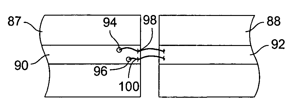
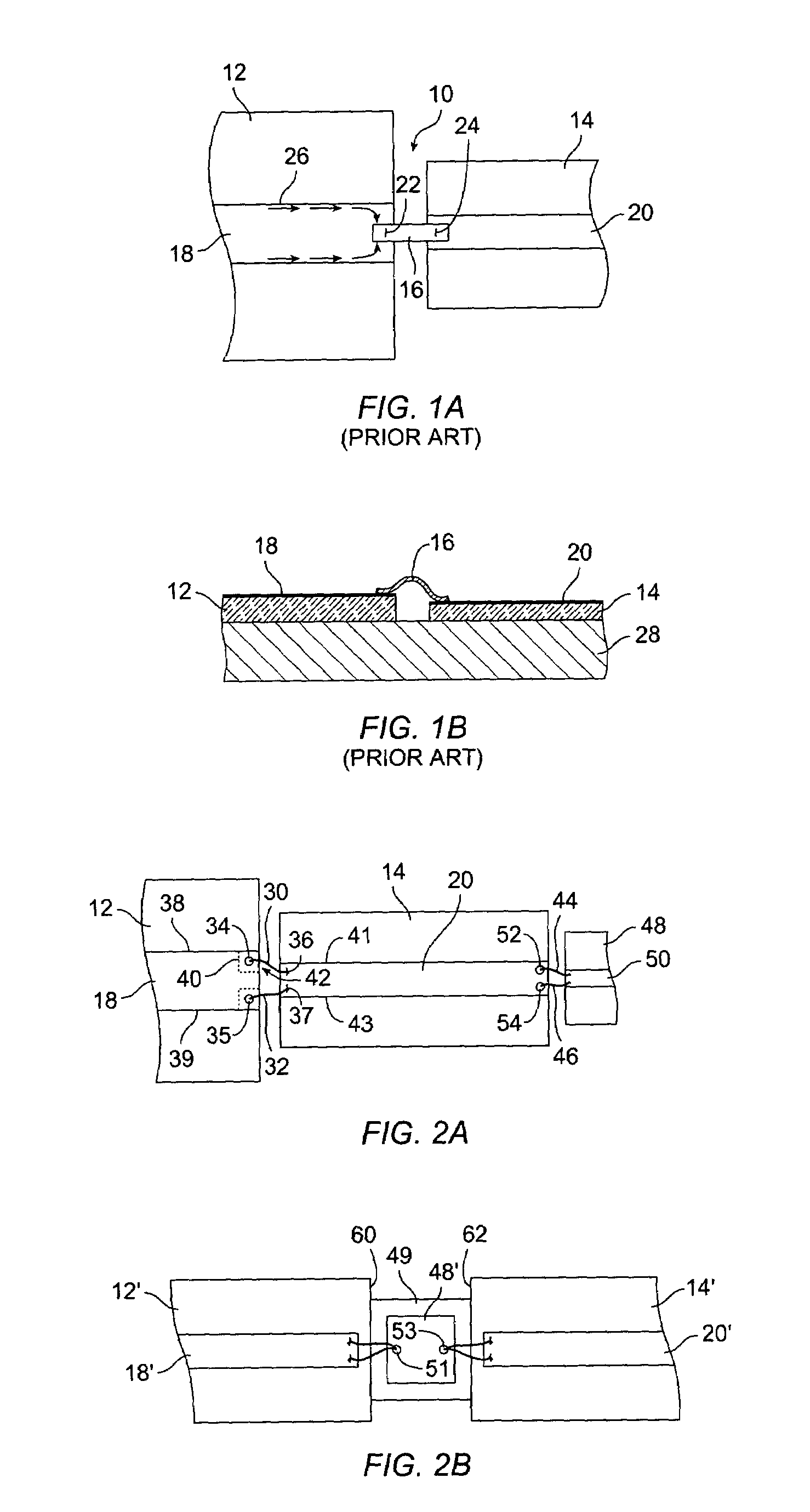
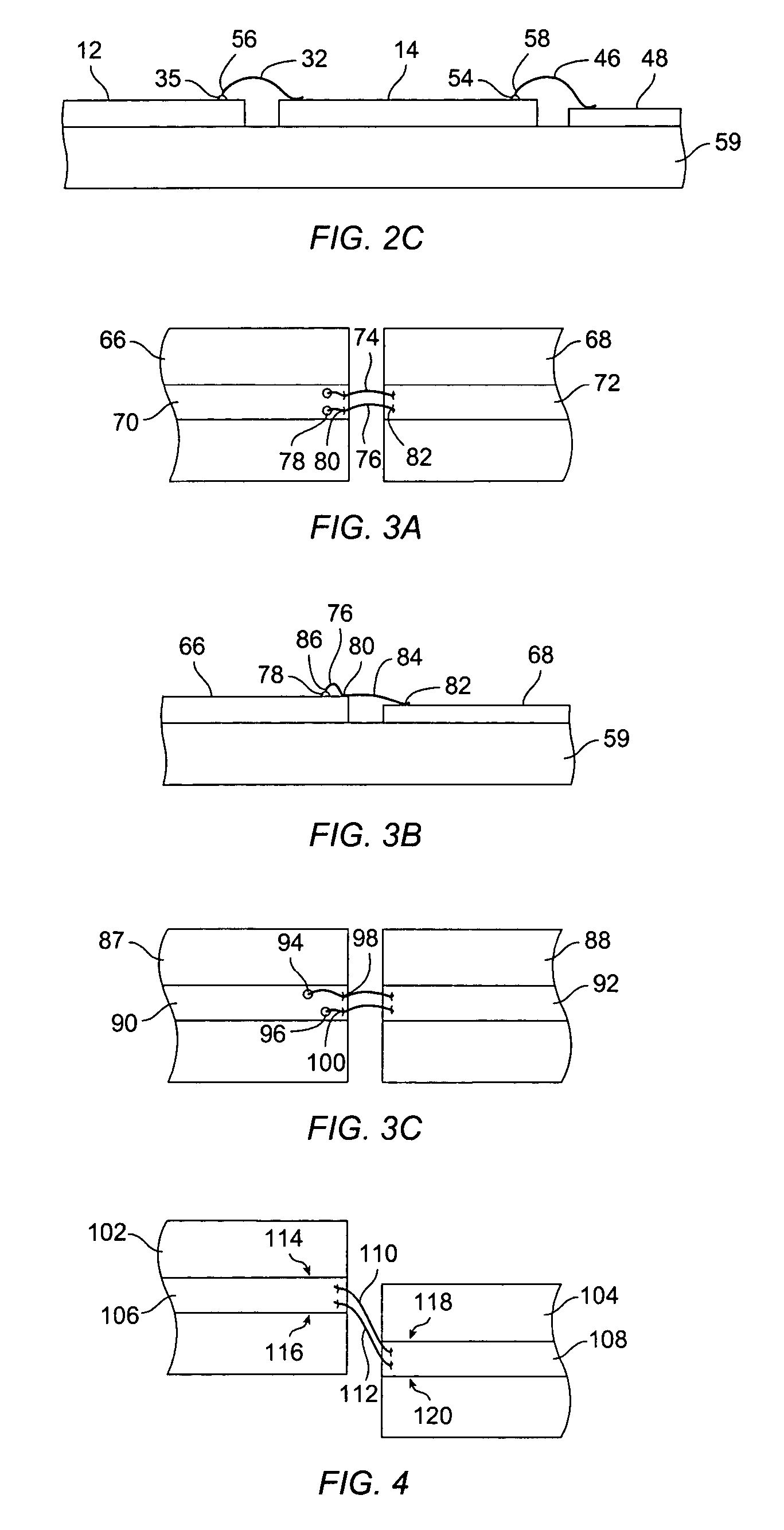
- The use of edge-to-edge bonding between center conductors of planar transmission lines or between these lines and other components, employing ball bonds and intermediate bonds to improve impedance continuity, with bond wires placed close to the edges of the conductors to minimize current flow disruptions.

Chip package and electrical connection structure between chip and substrate
PatentInactiveUS7129568B2
Innovation
- The introduction of a characterized lead structure with a larger cross-sectional area than generic leads, which induces a capacitative effect to compensate for the inductive effect of characterized wires, thereby matching the impedance of the transmission circuit with the system impedance.


EMC Compliance Standards for Copper Interconnects
Electromagnetic compatibility standards for copper interconnects establish critical requirements that directly impact the design choices between copper clip bonding and wire mesh layer implementations. The International Electrotechnical Commission (IEC) 61000 series provides comprehensive EMC guidelines, while regional standards such as FCC Part 15 in North America and EN 55032 in Europe define specific emission limits for electronic devices utilizing copper interconnection technologies.
The fundamental EMC compliance framework addresses both conducted and radiated emissions, with copper interconnects serving as potential sources of electromagnetic interference. Standards typically specify measurement methodologies using CISPR-compliant test equipment, establishing limits across frequency ranges from 150 kHz to 30 MHz for conducted emissions and 30 MHz to 1 GHz for radiated emissions. These frequency bands are particularly relevant when evaluating signal reflection characteristics in copper clip bonding versus wire mesh configurations.
Copper clip bonding implementations must comply with IEC 62153 standards for metallic communication cables, which define transfer impedance and screening attenuation requirements. The standard establishes maximum permissible surface transfer impedance values, typically ranging from 1 to 100 milliohms per meter depending on frequency and application category. Wire mesh layer configurations fall under similar scrutiny, with additional considerations for mesh density and conductor spacing affecting compliance margins.
Military and aerospace applications impose stricter requirements through MIL-STD-461 and DO-160 standards, demanding enhanced shielding effectiveness and reduced susceptibility levels. These standards require copper interconnects to demonstrate shielding effectiveness exceeding 60 dB across critical frequency ranges, directly influencing the selection between clip bonding and mesh layer approaches based on their respective electromagnetic performance characteristics.
Automotive industry compliance follows ISO 11452 and CISPR 25 standards, emphasizing immunity testing and emission control in harsh electromagnetic environments. The standards mandate specific test configurations for copper interconnect assemblies, including bulk current injection and radiated field immunity tests that reveal performance differences between bonding methodologies under standardized conditions.
The fundamental EMC compliance framework addresses both conducted and radiated emissions, with copper interconnects serving as potential sources of electromagnetic interference. Standards typically specify measurement methodologies using CISPR-compliant test equipment, establishing limits across frequency ranges from 150 kHz to 30 MHz for conducted emissions and 30 MHz to 1 GHz for radiated emissions. These frequency bands are particularly relevant when evaluating signal reflection characteristics in copper clip bonding versus wire mesh configurations.
Copper clip bonding implementations must comply with IEC 62153 standards for metallic communication cables, which define transfer impedance and screening attenuation requirements. The standard establishes maximum permissible surface transfer impedance values, typically ranging from 1 to 100 milliohms per meter depending on frequency and application category. Wire mesh layer configurations fall under similar scrutiny, with additional considerations for mesh density and conductor spacing affecting compliance margins.
Military and aerospace applications impose stricter requirements through MIL-STD-461 and DO-160 standards, demanding enhanced shielding effectiveness and reduced susceptibility levels. These standards require copper interconnects to demonstrate shielding effectiveness exceeding 60 dB across critical frequency ranges, directly influencing the selection between clip bonding and mesh layer approaches based on their respective electromagnetic performance characteristics.
Automotive industry compliance follows ISO 11452 and CISPR 25 standards, emphasizing immunity testing and emission control in harsh electromagnetic environments. The standards mandate specific test configurations for copper interconnect assemblies, including bulk current injection and radiated field immunity tests that reveal performance differences between bonding methodologies under standardized conditions.
Thermal Management Considerations in Copper Bonding
Thermal management represents a critical consideration in copper bonding applications, particularly when comparing copper clip bonding and wire mesh layer implementations. The fundamental thermal properties of copper, including its exceptional thermal conductivity of approximately 400 W/mK, make it an ideal material for heat dissipation in electronic packaging. However, the geometric configuration and bonding methodology significantly influence thermal performance characteristics.
Copper clip bonding configurations typically provide superior thermal pathways due to their solid metallic structure and direct contact interfaces. The continuous copper mass creates efficient heat conduction channels, enabling rapid thermal transfer from heat-generating components to heat sinks or thermal interface materials. The bonding process itself, whether through soldering, sintering, or mechanical attachment, establishes low thermal resistance connections that minimize temperature gradients across the interface.
Wire mesh layer implementations present different thermal management characteristics due to their inherently porous structure. While individual copper wires maintain excellent thermal conductivity, the air gaps between mesh elements introduce thermal resistance that can impede heat flow. The effective thermal conductivity of wire mesh configurations depends heavily on mesh density, wire diameter, and the presence of filling materials or thermal interface compounds within the mesh structure.
Temperature distribution patterns differ significantly between these two approaches. Copper clip bonding tends to create more uniform temperature profiles across the bonding interface, reducing hot spot formation and thermal stress concentrations. The solid copper structure facilitates multidirectional heat spreading, effectively distributing thermal loads across larger surface areas.
Thermal expansion considerations become particularly important in high-temperature applications. Copper's coefficient of thermal expansion must be carefully matched with substrate materials to prevent mechanical stress and potential delamination. Wire mesh configurations may offer some advantage in accommodating thermal expansion differences due to their flexible structure, while solid copper clips require more precise thermal expansion matching.
Manufacturing processes also influence thermal performance outcomes. Copper clip bonding processes often achieve better thermal interface quality through controlled pressure and temperature application during assembly. Wire mesh implementations may suffer from inconsistent thermal contact due to manufacturing variations in mesh uniformity and bonding material distribution throughout the mesh structure.
Copper clip bonding configurations typically provide superior thermal pathways due to their solid metallic structure and direct contact interfaces. The continuous copper mass creates efficient heat conduction channels, enabling rapid thermal transfer from heat-generating components to heat sinks or thermal interface materials. The bonding process itself, whether through soldering, sintering, or mechanical attachment, establishes low thermal resistance connections that minimize temperature gradients across the interface.
Wire mesh layer implementations present different thermal management characteristics due to their inherently porous structure. While individual copper wires maintain excellent thermal conductivity, the air gaps between mesh elements introduce thermal resistance that can impede heat flow. The effective thermal conductivity of wire mesh configurations depends heavily on mesh density, wire diameter, and the presence of filling materials or thermal interface compounds within the mesh structure.
Temperature distribution patterns differ significantly between these two approaches. Copper clip bonding tends to create more uniform temperature profiles across the bonding interface, reducing hot spot formation and thermal stress concentrations. The solid copper structure facilitates multidirectional heat spreading, effectively distributing thermal loads across larger surface areas.
Thermal expansion considerations become particularly important in high-temperature applications. Copper's coefficient of thermal expansion must be carefully matched with substrate materials to prevent mechanical stress and potential delamination. Wire mesh configurations may offer some advantage in accommodating thermal expansion differences due to their flexible structure, while solid copper clips require more precise thermal expansion matching.
Manufacturing processes also influence thermal performance outcomes. Copper clip bonding processes often achieve better thermal interface quality through controlled pressure and temperature application during assembly. Wire mesh implementations may suffer from inconsistent thermal contact due to manufacturing variations in mesh uniformity and bonding material distribution throughout the mesh structure.
Unlock deeper insights with Patsnap Eureka Quick Research — get a full tech report to explore trends and direct your research. Try now!
Generate Your Research Report Instantly with AI Agent
Supercharge your innovation with Patsnap Eureka AI Agent Platform!