

Redistribution Layer vs PCB: Which is More Cost-Effective?
APR 7, 20269 MIN READ
Generate Your Research Report Instantly with AI Agent
PatSnap Eureka helps you evaluate technical feasibility & market potential.
RDL vs PCB Technology Background and Objectives
The semiconductor packaging industry has undergone significant transformation over the past two decades, driven by the relentless demand for miniaturization, enhanced performance, and cost optimization. Traditional packaging approaches have evolved to accommodate increasingly complex integrated circuits while maintaining economic viability in high-volume manufacturing environments.
Redistribution Layer technology emerged as a revolutionary approach in advanced packaging, fundamentally altering how electrical connections are established between semiconductor dies and external interfaces. RDL utilizes thin-film processing techniques to create fine-pitch interconnections directly on the wafer or package substrate, enabling unprecedented routing flexibility and density. This technology has become particularly crucial in applications requiring ultra-compact form factors and high-frequency performance characteristics.
Printed Circuit Board technology represents the established foundation of electronic interconnection systems, having matured over several decades of continuous refinement. PCB manufacturing leverages well-established processes including photolithography, etching, and lamination to create multi-layer interconnection structures. The technology offers proven reliability, standardized manufacturing processes, and extensive supply chain infrastructure across global markets.
The convergence of market demands for smaller, faster, and more cost-effective electronic devices has intensified the need for comprehensive cost-effectiveness analysis between these two interconnection approaches. Modern applications spanning mobile devices, automotive electronics, and high-performance computing require careful evaluation of both immediate manufacturing costs and long-term performance benefits.
The primary objective of this comparative analysis centers on establishing quantitative frameworks for evaluating the total cost of ownership between RDL and PCB implementations. This encompasses direct manufacturing costs, yield considerations, performance implications, and scalability factors across different application domains and production volumes.
Secondary objectives include identifying optimal application scenarios for each technology, understanding the crossover points where one approach becomes more economically viable than the other, and projecting future cost trajectories based on technological maturation curves. The analysis aims to provide actionable insights for strategic technology selection in next-generation product development initiatives.
Market Demand for Advanced Packaging Solutions
The semiconductor industry is experiencing unprecedented demand for advanced packaging solutions, driven by the relentless pursuit of miniaturization, enhanced performance, and cost optimization across multiple application domains. This surge in demand stems from the fundamental limitations of traditional scaling approaches and the growing complexity of modern electronic systems.
Consumer electronics represent the largest market segment driving advanced packaging adoption. Smartphones, tablets, and wearable devices require increasingly sophisticated packaging technologies to accommodate multiple functionalities within constrained form factors. The integration of processors, memory, sensors, and communication modules necessitates packaging solutions that can deliver superior electrical performance while maintaining thermal efficiency and mechanical reliability.
The automotive sector has emerged as a significant growth driver, particularly with the accelerated adoption of electric vehicles and autonomous driving technologies. Advanced driver assistance systems, infotainment platforms, and battery management systems demand packaging solutions capable of operating under extreme environmental conditions while delivering high-speed data processing capabilities. The automotive industry's stringent reliability requirements have created substantial opportunities for advanced packaging technologies.
Data center and high-performance computing applications continue to fuel demand for sophisticated packaging solutions. The exponential growth in artificial intelligence, machine learning, and cloud computing workloads requires packaging technologies that can support massive parallel processing capabilities while managing thermal dissipation effectively. Server processors, graphics processing units, and specialized accelerators increasingly rely on advanced packaging to achieve target performance metrics.
The telecommunications infrastructure transformation, particularly the global deployment of 5G networks, has created substantial market opportunities. Base station equipment, network processors, and radio frequency components require packaging solutions that can handle high-frequency signals while maintaining signal integrity and minimizing power consumption.
Industrial automation and Internet of Things applications represent emerging market segments with significant growth potential. Smart manufacturing systems, industrial sensors, and edge computing devices require packaging solutions that balance performance requirements with cost constraints while ensuring long-term reliability in harsh operating environments.
Market dynamics indicate a clear preference shift toward packaging solutions that offer superior cost-effectiveness ratios. Manufacturers increasingly evaluate packaging technologies based on total cost of ownership rather than initial implementation costs, considering factors such as yield rates, assembly complexity, testing requirements, and long-term reliability performance.
Current State of RDL and PCB Manufacturing Technologies
Redistribution Layer (RDL) manufacturing has evolved significantly over the past decade, driven by the semiconductor industry's demand for advanced packaging solutions. Current RDL fabrication primarily employs photolithography-based processes, utilizing spin-coating techniques for dielectric layer deposition and sputtering or electroplating for metal layer formation. Leading foundries such as TSMC, Samsung, and ASE Group have established mature 2.5D and 3D packaging lines with RDL capabilities supporting line widths down to 2-5 micrometers. The technology enables high-density interconnections with typical layer thicknesses ranging from 2-10 micrometers for dielectrics and 1-5 micrometers for metal traces.
Modern RDL processes incorporate advanced materials including low-k dielectrics, copper metallization, and specialized photoresists optimized for fine-pitch applications. Manufacturing throughput has improved substantially, with current production lines achieving cycle times of 4-6 hours per wafer for multi-layer RDL structures. However, the technology faces constraints in terms of substrate warpage management, thermal stress control, and yield optimization for large die sizes exceeding 20mm x 20mm.
PCB manufacturing technology has simultaneously advanced, particularly in high-density interconnect (HDI) and embedded component technologies. Current state-of-the-art PCB fabrication supports trace widths down to 25-50 micrometers using modified semi-additive processes (mSAP) and advanced laser drilling techniques. Major manufacturers like Unimicron, Ibiden, and AT&S have invested heavily in next-generation equipment enabling layer counts exceeding 20 layers with controlled impedance tolerances within ±5%.
Contemporary PCB processes leverage improved materials including low-loss dielectrics, high-frequency laminates, and advanced copper foils with enhanced adhesion properties. Manufacturing scalability remains a key advantage, with panel-level processing enabling cost-effective production for larger form factors. Recent innovations include any-layer HDI structures and embedded active/passive components, bridging the gap between traditional PCB and advanced packaging technologies.
Both technologies continue facing challenges related to thermal management, signal integrity at high frequencies, and manufacturing cost optimization. The integration of artificial intelligence and machine learning in process control has begun improving yield rates and defect detection capabilities across both RDL and PCB manufacturing platforms.
Existing RDL and PCB Implementation Solutions
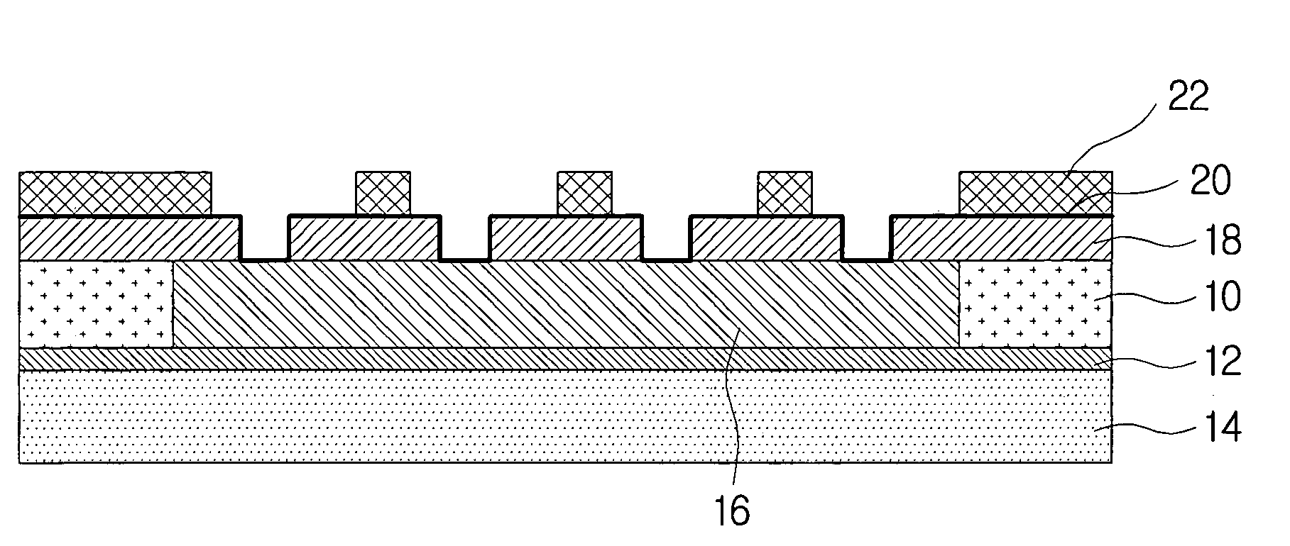
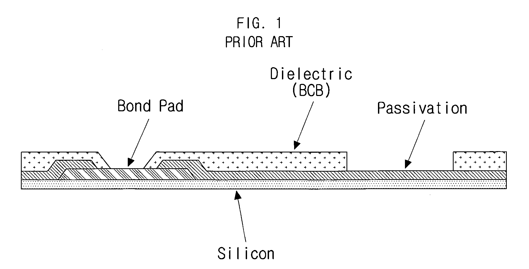
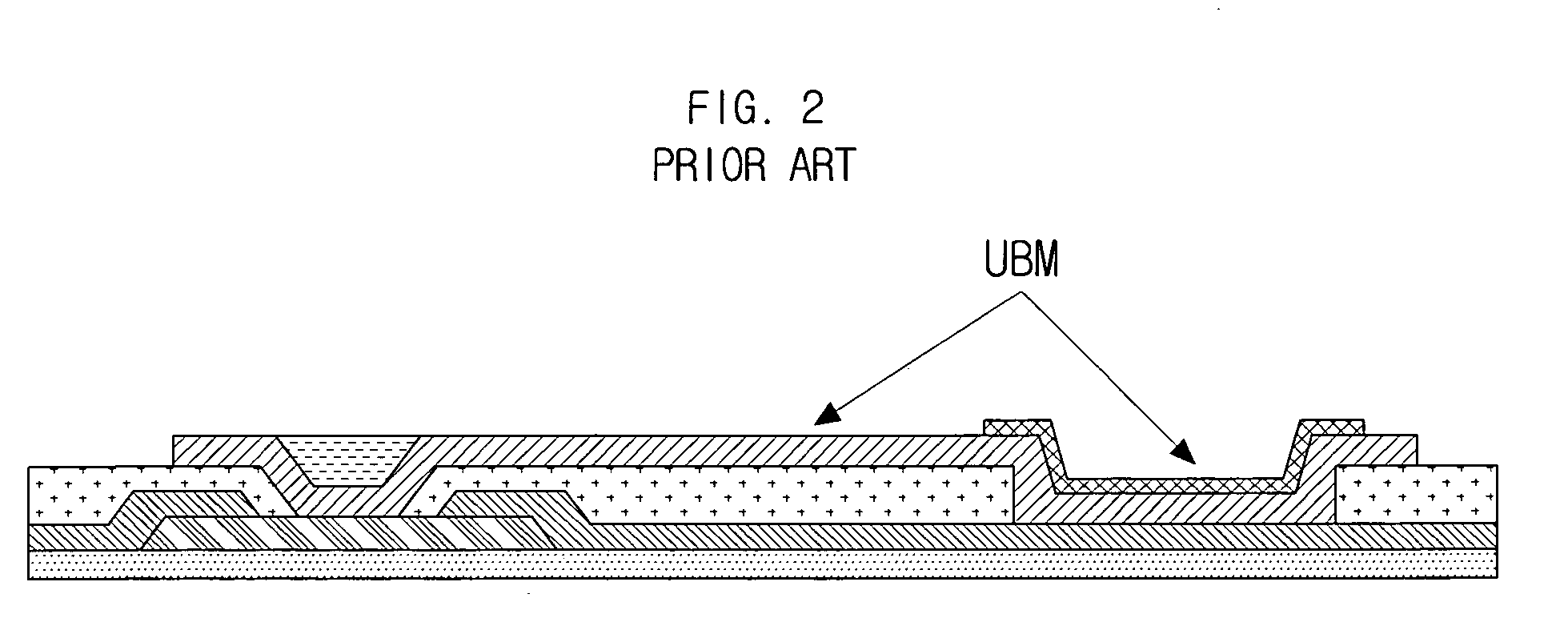
01 Redistribution layer structure for cost reduction
Redistribution layers (RDL) can be designed with optimized structures to reduce manufacturing costs while maintaining electrical performance. This includes using fewer metal layers, simplified routing patterns, and standardized design rules. The RDL approach can eliminate the need for traditional PCB substrates in certain applications, particularly in advanced packaging solutions, thereby reducing overall system costs through integration and miniaturization.- Redistribution layer structure for cost reduction: Redistribution layers (RDL) can be designed with optimized structures to reduce manufacturing costs while maintaining electrical performance. This includes using fewer metal layers, simplified routing patterns, and standardized design rules. The RDL approach can eliminate the need for traditional PCB substrates in certain applications, reducing overall package costs through integration of interconnect functions directly on the semiconductor die or package.
- Fan-out wafer level packaging with RDL for cost optimization: Fan-out wafer level packaging technology utilizing redistribution layers offers cost advantages over traditional PCB-based packaging by enabling higher integration density and eliminating substrate costs. This approach allows for direct connection of die to external contacts through redistribution layers, reducing the number of packaging components and assembly steps required. The technology enables cost-effective solutions for high-density interconnect applications.
- Hybrid substrate combining RDL and PCB technologies: Hybrid packaging solutions that combine redistribution layer technology with printed circuit board elements provide balanced cost-effectiveness by leveraging advantages of both approaches. This integration allows for fine-pitch connections through RDL in critical areas while using cost-effective PCB technology for less demanding interconnect regions. The hybrid approach optimizes material usage and manufacturing processes to achieve better cost-performance ratios.
- Material selection and process optimization for RDL cost reduction: Cost-effectiveness of redistribution layers can be improved through strategic material selection and manufacturing process optimization. This includes using alternative dielectric materials, optimized metal deposition techniques, and simplified patterning processes. Process innovations such as panel-level processing and batch fabrication methods can significantly reduce per-unit costs compared to traditional PCB manufacturing for high-volume applications.
- Design methodology for RDL versus PCB trade-off analysis: Systematic design methodologies enable evaluation of cost-effectiveness trade-offs between redistribution layer and PCB implementations. These approaches consider factors such as interconnect density requirements, electrical performance specifications, thermal management needs, and production volumes. Design tools and frameworks help determine optimal technology selection based on application-specific cost and performance requirements, including considerations for scalability and manufacturing yield.
02 Fan-out wafer level packaging with RDL for cost optimization
Fan-out wafer level packaging utilizing redistribution layers offers cost advantages over traditional PCB-based solutions by enabling higher integration density and reduced package size. This technology allows for direct chip-to-substrate connections without wire bonding, reducing material costs and improving electrical performance. The approach is particularly cost-effective for high-volume production where the initial tooling investment can be amortized across large quantities.Expand Specific Solutions03 Hybrid substrate combining RDL and PCB technologies
Hybrid substrate solutions that combine redistribution layer technology with traditional PCB structures provide a balanced approach to cost-effectiveness. This method leverages the fine-pitch capabilities of RDL for critical high-density interconnections while using conventional PCB technology for less demanding routing areas. The hybrid approach optimizes material usage and manufacturing processes to achieve cost savings while meeting performance requirements.Expand Specific Solutions04 Material selection and process optimization for RDL cost reduction
Cost-effectiveness in redistribution layer manufacturing can be achieved through strategic material selection and process optimization. This includes using alternative dielectric materials, optimized metal deposition techniques, and simplified photolithography processes. Manufacturing yield improvements and reduced processing steps contribute to lower production costs while maintaining reliability standards. The selection of appropriate materials and processes depends on the specific application requirements and production volume.Expand Specific Solutions05 Design methodology for RDL versus PCB cost comparison
Systematic design methodologies enable accurate cost comparison between redistribution layer and PCB solutions by considering factors such as layer count, via density, line width requirements, and manufacturing complexity. Design tools and simulation methods help optimize the trade-offs between performance, size, and cost. The analysis includes consideration of non-recurring engineering costs, production volume, and lifecycle costs to determine the most cost-effective solution for specific applications.Expand Specific Solutions
Key Players in RDL and PCB Manufacturing Industry
The cost-effectiveness comparison between Redistribution Layer (RDL) and PCB technologies represents a rapidly evolving segment within the semiconductor packaging industry, currently in a growth phase driven by miniaturization demands and advanced packaging requirements. The market demonstrates significant expansion potential, particularly in mobile and high-performance computing applications, with estimated values reaching billions annually. Technology maturity varies considerably across market players, with established leaders like Samsung Electronics, TSMC, and Intel driving advanced RDL implementations for cutting-edge applications, while companies such as Advanced Semiconductor Engineering, Powertech Technology, and Yamaichi Electronics focus on optimizing traditional PCB solutions and hybrid approaches. The competitive landscape shows clear segmentation between foundries pursuing next-generation RDL technologies for premium applications and assembly service providers enhancing PCB cost-efficiency for mainstream products, creating distinct value propositions across different market segments.
Samsung Electronics Co., Ltd.
Technical Solution: Samsung has invested heavily in advanced packaging technologies featuring redistribution layers for their memory and processor products. Their Package-on-Package (PoP) and System-in-Package (SiP) solutions utilize multi-layer RDL structures to achieve high-density interconnections while reducing overall package size. Samsung's cost analysis indicates that RDL-based packages provide 25-35% better space efficiency compared to traditional PCB solutions, making them particularly attractive for mobile applications where miniaturization is critical. However, their studies show PCB remains more cost-effective for applications requiring fewer than 200 I/O connections, while RDL becomes advantageous for higher pin counts and tighter pitch requirements.
Strengths: Strong integration capabilities, proven high-volume manufacturing, excellent miniaturization. Weaknesses: Higher tooling costs, longer development cycles compared to PCB solutions.
Taiwan Semiconductor Manufacturing Co., Ltd.
Technical Solution: TSMC has developed advanced packaging solutions including Chip-on-Wafer-on-Substrate (CoWoS) and Integrated Fan-Out (InFO) technologies that utilize redistribution layers for high-density interconnections. Their CoWoS technology employs silicon interposers with fine-pitch RDL to achieve superior electrical performance compared to traditional PCB solutions. The company's InFO packaging uses polymer-based RDL structures that provide cost advantages over silicon interposers while maintaining better signal integrity than standard PCB approaches. TSMC's analysis shows RDL solutions can reduce package footprint by 30-40% compared to equivalent PCB implementations, though at higher manufacturing costs for low-volume applications.
Strengths: Industry-leading RDL manufacturing capabilities, superior electrical performance, compact form factors. Weaknesses: Higher initial costs, complex manufacturing processes requiring specialized equipment.
Core Cost Analysis Methods for RDL vs PCB
Method of manufacturing wafer level package
PatentInactiveUS7632709B2
Innovation
- The method involves forming the first redistribution layer using semiconductor processes and subsequent layers using PCB processes, reducing costs by leveraging low-cost PCB processes for increased stability and efficiency, including steps like stacking an insulation layer, forming a seed layer, electroplating a redistribution pattern, and coupling conductive balls after passivation.

Printed circuit board, fabrication method thereof and mainboard of terminal product
PatentActiveEP1981314B1
Innovation
- A four-layer printed circuit board design with outer surface layers acting as primary grounds interconnected through vias, and inner layers arranged for signal wiring by functional areas, reducing the interlayer distance and optimizing line width and height to control impedance and crosstalk, thereby simplifying the fabrication process and reducing material usage.


Supply Chain Impact on RDL and PCB Economics
The supply chain dynamics significantly influence the economic viability of both Redistribution Layer (RDL) and PCB technologies, creating distinct cost structures and market positioning strategies. RDL technology relies heavily on advanced semiconductor fabrication facilities, which are concentrated in specific geographic regions, primarily in Asia-Pacific countries including Taiwan, South Korea, and Japan. This concentration creates supply chain vulnerabilities but also enables economies of scale within established semiconductor ecosystems.
PCB manufacturing benefits from a more distributed global supply chain with production facilities spanning across China, Southeast Asia, Europe, and North America. This geographic diversification provides greater supply chain resilience and flexibility in sourcing strategies. The PCB supply chain encompasses a broader range of material suppliers, from copper foil and fiberglass manufacturers to specialty chemical providers, creating multiple sourcing options and competitive pricing dynamics.
Raw material costs represent a critical differentiator between the two technologies. RDL processes require high-purity silicon wafers, specialized photoresists, and advanced metallization materials, which command premium pricing due to stringent quality requirements and limited supplier bases. The semiconductor-grade materials used in RDL fabrication are subject to longer lead times and higher inventory carrying costs, impacting overall economic efficiency.
PCB supply chains benefit from mature material ecosystems with standardized specifications and multiple qualified suppliers. Commodity materials such as FR-4 substrates, copper, and standard solder masks are readily available with shorter lead times and more predictable pricing structures. This maturity enables just-in-time manufacturing approaches and reduces working capital requirements.
Supply chain scalability presents another economic consideration. RDL production scaling requires significant capital investments in specialized equipment and cleanroom facilities, creating barriers to rapid capacity expansion. PCB manufacturing can achieve scalability through distributed production networks and standardized equipment, enabling more flexible capacity management and reduced capital intensity per unit of output.
Environmental Considerations in Packaging Technology Selection
Environmental considerations have become increasingly critical in packaging technology selection as the electronics industry faces mounting pressure to reduce its ecological footprint. The choice between Redistribution Layer (RDL) and traditional PCB technologies carries significant environmental implications that extend beyond immediate cost considerations to encompass lifecycle environmental impact, resource consumption, and end-of-life disposal challenges.
Material consumption patterns differ substantially between RDL and PCB manufacturing processes. RDL technology typically requires fewer raw materials due to its thinner profile and more efficient use of conductive materials. The wafer-level processing approach minimizes material waste through precise deposition techniques, contrasting with PCB manufacturing which involves subtractive processes that generate considerable copper and substrate waste. Additionally, RDL processes often utilize advanced materials with lower environmental impact profiles, including lead-free solders and halogen-free substrates that align with international environmental regulations.
Energy consumption during manufacturing represents another crucial environmental factor. RDL fabrication leverages semiconductor processing equipment that, while energy-intensive per unit time, achieves higher throughput and efficiency compared to traditional PCB manufacturing lines. The consolidated processing steps in RDL production reduce overall energy consumption per unit, particularly when considering the elimination of separate assembly processes required for discrete components on PCBs.
Waste generation and chemical usage patterns vary significantly between these technologies. PCB manufacturing involves extensive use of etching chemicals, plating solutions, and cleaning agents that require careful disposal and treatment. RDL processes, while still requiring specialized chemicals, typically generate less liquid waste due to their precision deposition methods and reduced processing steps. The photolithographic processes used in RDL manufacturing also enable better chemical recovery and recycling opportunities.
End-of-life considerations favor RDL technology in several aspects. The reduced material complexity and smaller form factors of RDL-based packages facilitate more efficient recycling processes. The higher integration density achievable with RDL technology also means fewer individual components require disposal, reducing the overall environmental burden of electronic waste. However, the advanced materials used in some RDL applications may present specialized recycling challenges that require dedicated processing facilities.
Regulatory compliance and environmental certifications increasingly influence technology selection decisions. Both RDL and PCB technologies must meet stringent environmental standards, but RDL's newer development trajectory often incorporates environmental considerations from the design phase, potentially offering advantages in meeting future regulatory requirements and sustainability targets.
Unlock deeper insights with PatSnap Eureka Quick Research — get a full tech report to explore trends and direct your research. Try now!
Generate Your Research Report Instantly with AI Agent
Supercharge your innovation with PatSnap Eureka AI Agent Platform!