

Crystal Bridging vs Annealing: A Comparative Study
MAR 19, 20269 MIN READ
Generate Your Research Report Instantly with AI Agent
PatSnap Eureka helps you evaluate technical feasibility & market potential.
Crystal Bridging and Annealing Background and Objectives
Crystal bridging and annealing represent two fundamental approaches to material processing and structural modification, each with distinct mechanisms and applications across various industries. Crystal bridging involves the formation of crystalline connections between particles or surfaces, creating continuous pathways that enhance mechanical, electrical, or thermal properties. This phenomenon occurs through controlled nucleation and growth processes, where crystalline phases develop at interfaces to establish robust interconnections.
Annealing, conversely, is a thermal treatment process designed to alter material properties through controlled heating and cooling cycles. This technique relieves internal stresses, promotes recrystallization, and optimizes grain structure to achieve desired mechanical and physical characteristics. The process has evolved from traditional metallurgical applications to encompass semiconductors, ceramics, and advanced composite materials.
The historical development of these technologies traces back to early metallurgy for annealing, while crystal bridging emerged from advances in materials science and nanotechnology. Both approaches have gained significant attention due to increasing demands for high-performance materials in electronics, aerospace, automotive, and energy storage applications. The convergence of these fields has created opportunities for hybrid processing strategies that leverage advantages of both techniques.
Current technological objectives focus on optimizing processing parameters to achieve superior material properties while maintaining cost-effectiveness and scalability. For crystal bridging, primary goals include controlling nucleation sites, managing growth kinetics, and ensuring uniform distribution of crystalline connections. Annealing objectives center on precise temperature control, atmosphere management, and time optimization to achieve target microstructures.
The comparative study of these approaches aims to establish comprehensive understanding of their respective strengths, limitations, and optimal application domains. This research seeks to identify synergistic opportunities where combined implementation could yield enhanced performance beyond individual techniques. Additionally, the study addresses energy efficiency considerations, processing time requirements, and equipment complexity factors that influence industrial adoption decisions.
Emerging applications in flexible electronics, energy storage devices, and advanced ceramics have intensified interest in both crystal bridging and annealing technologies. The development of in-situ monitoring techniques and process control systems has enabled more precise implementation of these approaches, leading to improved reproducibility and quality outcomes.
Market Demand for Advanced Crystal Processing Technologies
The semiconductor and electronics manufacturing industries are experiencing unprecedented demand for advanced crystal processing technologies, driven by the exponential growth in high-performance computing, artificial intelligence, and next-generation communication systems. Crystal bridging and annealing processes have emerged as critical technologies for addressing defect mitigation, stress relief, and structural optimization in semiconductor devices. The market demand stems from the industry's relentless pursuit of smaller feature sizes, higher device densities, and improved electrical performance characteristics.
Consumer electronics manufacturers are increasingly requiring sophisticated crystal processing solutions to meet the stringent quality standards of modern devices. The proliferation of 5G infrastructure, Internet of Things applications, and autonomous vehicle systems has created substantial market pressure for enhanced crystal quality and reliability. These applications demand materials with superior electrical properties, thermal stability, and mechanical integrity that can only be achieved through advanced processing techniques.
The photovoltaic industry represents another significant market driver for crystal processing technologies. Solar cell manufacturers are seeking cost-effective methods to improve crystal structure uniformity and reduce defect densities in silicon wafers. Both crystal bridging and annealing techniques offer potential solutions for enhancing photovoltaic conversion efficiency while maintaining manufacturing scalability and economic viability.
Emerging applications in quantum computing and advanced sensor technologies are creating new market segments with specialized requirements for ultra-high-purity crystals. These applications demand precise control over crystal defects, grain boundaries, and stress distributions, positioning advanced processing technologies as enablers for next-generation technological breakthroughs.
The aerospace and defense sectors are driving demand for crystal processing technologies capable of producing materials with exceptional reliability under extreme operating conditions. Military and space applications require crystals with enhanced radiation resistance, thermal cycling durability, and long-term stability characteristics.
Market growth is further accelerated by the increasing adoption of wide-bandgap semiconductors, including silicon carbide and gallium nitride materials. These materials present unique processing challenges that traditional techniques cannot adequately address, creating opportunities for innovative crystal processing approaches that combine bridging and annealing methodologies to optimize material properties and manufacturing yields.
Current State and Challenges in Crystal Formation Methods
Crystal formation methods have evolved significantly over the past decades, with crystal bridging and annealing emerging as two prominent approaches for controlling crystalline structure and properties. Currently, both techniques are widely employed across semiconductor manufacturing, pharmaceutical crystallization, and advanced materials synthesis, yet each faces distinct technological limitations that constrain their broader application.
Crystal bridging technology has reached a mature state in specific applications, particularly in semiconductor device fabrication where precise control over grain boundaries is critical. The method excels in creating controlled connections between crystal domains, enabling enhanced electrical conductivity and mechanical strength. However, current bridging techniques struggle with scalability issues, as maintaining uniform bridging conditions across large substrate areas remains technically challenging. Temperature gradients and localized stress concentrations often lead to inconsistent bridging quality, resulting in variable material properties.
Annealing processes, while more established, face their own set of constraints. Traditional thermal annealing requires extended processing times and high energy consumption, making it economically unfavorable for large-scale production. Advanced annealing variants, including rapid thermal annealing and laser annealing, have addressed some timing concerns but introduce new challenges related to thermal shock and non-uniform heating patterns. The precise control of annealing atmospheres and temperature profiles remains a significant technical hurdle.
Both methods encounter fundamental challenges in achieving optimal crystal quality while maintaining process efficiency. Crystal bridging suffers from limited understanding of the underlying nucleation mechanisms, particularly in complex multi-component systems. The formation of unwanted secondary phases during bridging can compromise final material properties. Similarly, annealing processes often result in grain coarsening beyond desired specifications, leading to degraded mechanical properties in certain applications.
Geographically, crystal bridging research is concentrated in advanced semiconductor manufacturing regions, including Taiwan, South Korea, and specific areas in the United States and Europe. Annealing technology development shows broader global distribution, with significant contributions from Japan, Germany, and emerging research centers in China and India.
The integration of real-time monitoring and control systems represents a common challenge for both approaches. Current characterization techniques often lack the temporal resolution needed to optimize process parameters dynamically, limiting the ability to achieve consistent, high-quality crystal formation across different material systems and processing conditions.
Existing Crystal Bridging and Annealing Solutions
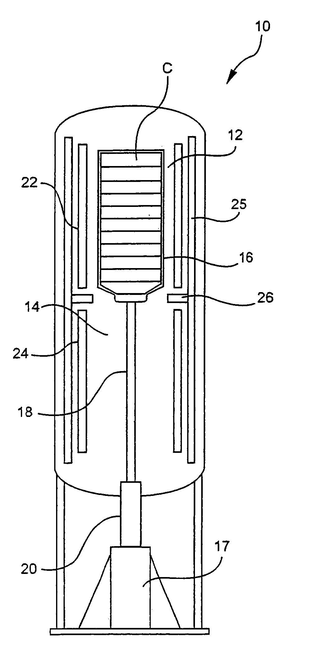
01 Annealing processes for crystalline materials
Various annealing techniques are employed to improve the crystalline structure and properties of materials. These processes involve controlled heating and cooling cycles to reduce internal stresses, eliminate defects, and enhance crystal formation. The annealing temperature, duration, and atmosphere are carefully controlled to achieve desired material properties such as improved mechanical strength, electrical conductivity, or optical characteristics.- Annealing processes for polymer materials: Annealing techniques are applied to polymer materials to improve their crystalline structure and mechanical properties. The process involves heating the material to specific temperatures and controlled cooling to reduce internal stresses and enhance crystal formation. This method is particularly effective for thermoplastic materials where controlled crystallization is desired to achieve optimal physical properties.
- Crystal bridging in fiber and film structures: Crystal bridging refers to the formation of crystalline connections between polymer chains or domains, which enhances the structural integrity and strength of fibers and films. This phenomenon occurs during processing or post-treatment steps and is crucial for improving tensile strength and dimensional stability. The bridging effect can be controlled through temperature, time, and mechanical stress parameters.
- Heat treatment methods for crystalline materials: Various heat treatment methods are employed to control crystallization and improve material properties. These methods include step-wise annealing, isothermal treatments, and gradient heating processes. The treatments are designed to optimize crystal size, distribution, and orientation, which directly affect the final product's performance characteristics such as clarity, strength, and thermal stability.
- Equipment and apparatus for annealing operations: Specialized equipment and apparatus have been developed for conducting annealing operations with precise temperature and atmosphere control. These systems include heating chambers, temperature control units, and cooling mechanisms designed to achieve uniform heat distribution and controlled cooling rates. The equipment enables reproducible processing conditions for consistent product quality.
- Applications in composite and multilayer structures: Crystal bridging and annealing techniques are applied to composite and multilayer structures to enhance interfacial bonding and overall structural performance. The processes facilitate the formation of crystalline connections across layer boundaries, improving adhesion and mechanical properties. These methods are particularly important in advanced materials where multiple layers with different properties need to be integrated effectively.
02 Crystal bridging in semiconductor devices
Crystal bridging techniques are utilized in semiconductor manufacturing to create electrical connections or structural links between different crystalline regions. This involves forming crystalline bridges that maintain lattice continuity across interfaces, which is crucial for device performance. The process may include epitaxial growth, recrystallization, or solid-phase crystallization methods to achieve proper crystal orientation and minimize defects at the bridging regions.Expand Specific Solutions03 Thermal treatment for crystal structure modification
Thermal treatment methods are applied to modify crystal structures through controlled heating processes. These techniques involve specific temperature profiles and holding times to induce phase transformations, grain growth, or recrystallization. The thermal treatment can be performed in various atmospheres including inert gases, vacuum, or reactive environments to achieve desired crystallographic changes while preventing unwanted oxidation or contamination.Expand Specific Solutions04 Crystal bridging in polymer and composite materials
In polymer and composite systems, crystal bridging refers to the formation of crystalline connections between different phases or regions. This phenomenon enhances mechanical properties by creating load-bearing pathways through crystalline structures. The bridging can occur during processing through controlled crystallization, where polymer chains or reinforcing materials form interconnected crystalline networks that improve strength, stiffness, and dimensional stability.Expand Specific Solutions05 Annealing equipment and apparatus design
Specialized equipment and apparatus are designed for performing annealing and crystal treatment processes. These systems include furnaces with precise temperature control, atmosphere management capabilities, and uniform heating zones. The equipment may feature multiple heating chambers, controlled cooling systems, and monitoring devices to ensure consistent processing conditions. Design considerations include energy efficiency, throughput optimization, and the ability to handle various material types and sizes.Expand Specific Solutions
Key Players in Crystal Processing and Materials Industry
The crystal bridging versus annealing technology landscape represents a mature semiconductor processing sector experiencing steady growth, with market size driven by increasing demand for advanced materials in electronics and photonics applications. The industry demonstrates high technical maturity, evidenced by established players like Corning Inc. and Applied Materials leading in specialized glass and materials engineering, while semiconductor giants including Taiwan Semiconductor Manufacturing Co., Micron Technology, and IBM drive innovation in crystal processing techniques. Asian manufacturers such as Sumitomo Electric Industries, Sharp Corp., and TanKeBlue Semiconductor contribute significant expertise in crystal growth and processing technologies. The competitive environment features both traditional materials companies and cutting-edge semiconductor foundries, with research institutions like Nanjing University of Science & Technology and Japan Science & Technology Agency supporting fundamental research. Technology maturity varies across applications, with established annealing processes being well-developed while advanced crystal bridging techniques continue evolving for next-generation semiconductor and optical device manufacturing.
Micron Technology, Inc.
Technical Solution: Micron has developed specialized crystal bridging techniques for memory device manufacturing, particularly for 3D NAND flash and DRAM applications. Their approach focuses on creating high-quality crystalline interfaces between different material layers while minimizing thermal budget impact on underlying structures. The company employs a combination of laser annealing and controlled crystal bridging to achieve optimal grain structure and electrical properties. Micron's process utilizes millisecond-duration laser pulses to selectively activate crystal growth while maintaining low substrate temperatures. This technique enables better control over crystal orientation and reduces defect density compared to conventional furnace annealing. Their crystal bridging methodology is specifically optimized for high-aspect-ratio structures common in 3D memory architectures, ensuring uniform crystal quality throughout the device stack.
Strengths: Specialized memory device expertise, innovative laser-based processing, excellent scalability for 3D structures. Weaknesses: Limited to memory applications, requires precise laser control systems.
Applied Materials, Inc.
Technical Solution: Applied Materials has developed advanced crystal bridging technologies for semiconductor manufacturing, utilizing plasma-enhanced chemical vapor deposition (PECVD) and atomic layer deposition (ALD) processes to create precise crystal structures. Their approach focuses on controlled nucleation and growth mechanisms that enable superior crystal bridging compared to traditional annealing methods. The company's Endura platform integrates multiple process chambers for sequential crystal formation steps, allowing for better control over crystal defects and grain boundaries. Their crystal bridging process operates at lower temperatures (300-400°C) compared to conventional annealing (800-1000°C), reducing thermal stress and improving device reliability. The technology incorporates real-time monitoring systems to optimize crystal formation parameters and ensure consistent quality across wafer batches.
Strengths: Industry-leading equipment reliability, comprehensive process control, lower temperature processing reduces thermal budget. Weaknesses: High capital equipment costs, complex process integration requirements.
Core Innovations in Crystal Structure Control Technologies
Crystal growth methods
PatentInactiveUS20040154527A1
Innovation
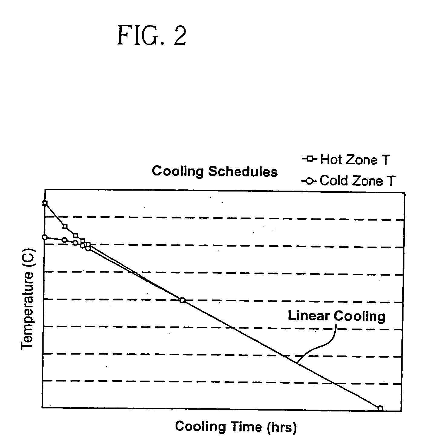
- A method involving in-situ annealing with a substantially constant cooling rate during the annealing process, specifically controlling temperature gradients and cooling rates to minimize stress and birefringence, allowing for the production of high-quality calcium fluoride crystals with reduced homogeneity and birefringence.
Crystal growth and annealing for minimized residual stress
PatentInactiveUS6350310B1
Innovation
- A method and apparatus that minimize temperature gradients during the annealing phase of crystal production, maintaining a uniform temperature to reduce residual stress and birefringence, using a thermal control system to manage temperature gradients during crystal growth and annealing.


Material Safety and Environmental Impact Assessment
Material safety considerations for crystal bridging and annealing processes present distinct risk profiles that require comprehensive evaluation. Crystal bridging operations typically involve controlled crystallization environments with specific temperature and pressure parameters, while annealing processes require sustained high-temperature exposure over extended periods. Both techniques utilize various chemical precursors and solvents that may pose inhalation, dermal contact, or fire hazards to personnel.
The primary safety concerns in crystal bridging include exposure to organic solvents used in solution-based crystallization methods, potential release of volatile compounds during controlled evaporation, and risks associated with pressure vessel operations in hydrothermal synthesis. Workers may encounter respiratory hazards from solvent vapors and particulate matter generated during crystal handling and processing stages.
Annealing processes present elevated risks due to prolonged high-temperature operations, typically ranging from 400°C to 1200°C depending on material specifications. These conditions create significant thermal hazards, potential exposure to metal oxides or ceramic dust, and risks from furnace atmospheres that may contain inert gases or reducing agents. Proper ventilation systems and personal protective equipment are essential to mitigate exposure to airborne contaminants generated during thermal treatment cycles.
Environmental impact assessment reveals that crystal bridging generally demonstrates superior environmental performance due to lower energy consumption and reduced greenhouse gas emissions. The process typically operates at ambient or moderately elevated temperatures, resulting in significantly lower carbon footprint compared to energy-intensive annealing operations. However, crystal bridging may generate liquid waste streams containing organic solvents that require specialized treatment and disposal protocols.
Annealing processes contribute substantially to environmental burden through high energy consumption, particularly when using electric or gas-fired furnaces for extended heating cycles. The carbon intensity of annealing operations depends heavily on local energy grid composition and furnace efficiency ratings. Additionally, some annealing atmospheres may release nitrogen oxides or other combustion byproducts that contribute to air quality degradation.
Waste management strategies differ significantly between the two approaches. Crystal bridging generates primarily liquid waste requiring solvent recovery or hazardous waste disposal, while annealing produces minimal direct waste but consumes substantial energy resources. Life cycle assessment studies indicate that crystal bridging typically achieves 40-60% lower environmental impact scores when considering energy consumption, emissions, and waste generation across the complete process chain.
Quality Standards and Performance Metrics for Crystal Processing
Quality standards for crystal processing encompass multiple dimensional parameters that directly impact the effectiveness of both crystal bridging and annealing techniques. The primary metrics include crystal lattice uniformity, measured through X-ray diffraction analysis with acceptable deviation ranges typically below 0.5% for high-grade applications. Surface roughness parameters, quantified using atomic force microscopy, must maintain Ra values under 10 nanometers for optimal performance in semiconductor applications.
Defect density serves as a critical performance indicator, with industry standards requiring dislocation densities below 10^4 cm^-2 for premium crystal substrates. Threading dislocation measurements utilize specialized etching techniques followed by optical microscopy analysis. Point defect concentrations, particularly oxygen and carbon impurities, are monitored through infrared spectroscopy with acceptable limits varying based on intended applications.
Thermal stability metrics evaluate crystal performance under operational conditions. Temperature coefficient measurements assess dimensional changes across operating ranges, with acceptable variations typically limited to parts per million per degree Celsius. Thermal shock resistance testing involves rapid temperature cycling protocols to validate structural integrity under stress conditions.
Mechanical property standards include hardness measurements using nanoindentation techniques, with values compared against established material databases. Fracture toughness testing employs controlled crack propagation methods to determine critical stress intensity factors. These mechanical parameters directly correlate with processing method effectiveness and long-term reliability.
Electrical characterization standards focus on resistivity uniformity across crystal surfaces, measured through four-point probe techniques with mapping resolution requirements. Carrier mobility and lifetime measurements utilize Hall effect analysis and photoconductivity decay methods respectively. These electrical properties serve as key indicators of crystal quality and processing optimization.
Optical quality metrics encompass transmission measurements across relevant wavelength ranges, with specifications varying by application requirements. Birefringence measurements using polarized light microscopy ensure optical uniformity. Surface optical scatter measurements quantify light scattering characteristics critical for photonic applications.
Contamination control standards establish acceptable limits for metallic and organic impurities, typically measured through secondary ion mass spectrometry and total reflection X-ray fluorescence techniques. Particle contamination levels are monitored using laser particle counters with size distribution analysis capabilities.
Unlock deeper insights with PatSnap Eureka Quick Research — get a full tech report to explore trends and direct your research. Try now!
Generate Your Research Report Instantly with AI Agent
Supercharge your innovation with PatSnap Eureka AI Agent Platform!