

Designing Compact Systems Using Gallium Nitride for Power Conversion Efficiency
JUN 17, 20269 MIN READ
Generate Your Research Report Instantly with AI Agent
Patsnap Eureka helps you evaluate technical feasibility & market potential.
GaN Power Conversion Background and Objectives
Gallium Nitride (GaN) technology represents a paradigm shift in power electronics, emerging from decades of semiconductor research that began in the 1960s. Unlike traditional silicon-based power devices, GaN offers superior material properties including a wider bandgap of 3.4 eV, higher breakdown field strength, and exceptional electron mobility. These fundamental characteristics enable power conversion systems to operate at higher frequencies, voltages, and temperatures while maintaining superior efficiency levels.
The evolution of GaN power devices has been driven by the increasing demand for compact, efficient power conversion solutions across multiple industries. From consumer electronics requiring smaller chargers to electric vehicles demanding lightweight power systems, the market has consistently pushed for technologies that can deliver more power in smaller form factors. Traditional silicon-based solutions have approached their theoretical limits, creating a technological gap that GaN technology is uniquely positioned to fill.
Historical development milestones in GaN power conversion trace back to early research in wide bandgap semiconductors, with significant commercial breakthroughs occurring in the 2010s. The technology has progressed from laboratory demonstrations to mass production, with manufacturing costs steadily declining and reliability metrics improving. Key technological advances include the development of enhancement-mode GaN transistors, improved thermal management solutions, and advanced packaging techniques that maximize the inherent benefits of GaN materials.
The primary objective of implementing GaN in compact power conversion systems centers on achieving unprecedented power density while maintaining high efficiency levels exceeding 95%. This involves overcoming traditional trade-offs between size, efficiency, and thermal performance that have constrained silicon-based designs. Target applications span from high-frequency switching power supplies and motor drives to renewable energy inverters and data center power infrastructure.
Technical objectives include developing GaN-based systems capable of operating at switching frequencies above 1 MHz, enabling significant reduction in passive component sizes. Additionally, the goal encompasses creating robust thermal management strategies that leverage GaN's superior thermal characteristics while addressing challenges related to localized heating and thermal cycling. Integration objectives focus on developing comprehensive system-level solutions that fully exploit GaN's capabilities rather than simply replacing silicon components.
The strategic vision for GaN power conversion technology extends beyond immediate performance improvements to enable entirely new applications and market segments. This includes ultra-compact power adapters, high-power-density electric vehicle chargers, and advanced grid-tied energy storage systems that were previously impractical with conventional semiconductor technologies.
Market Demand for Compact High-Efficiency Power Systems
The global power electronics market is experiencing unprecedented growth driven by the increasing demand for energy-efficient solutions across multiple industries. Consumer electronics manufacturers are under intense pressure to develop smaller, lighter devices without compromising performance, creating substantial demand for compact power conversion systems. The proliferation of smartphones, tablets, laptops, and wearable devices has established miniaturization as a critical market differentiator, with gallium nitride technology emerging as a key enabler for achieving these design objectives.
Electric vehicle adoption is accelerating worldwide, creating massive demand for high-efficiency power conversion systems that can maximize battery range while minimizing weight and thermal management requirements. Automotive manufacturers are actively seeking power electronics solutions that can deliver superior performance in increasingly constrained spaces, particularly for onboard chargers, DC-DC converters, and motor drive systems. The automotive sector's stringent reliability requirements and cost sensitivity are driving innovation in gallium nitride-based power systems.
Data center operators face mounting pressure to improve energy efficiency while accommodating exponentially growing computational demands. Server power supplies, voltage regulators, and power distribution systems require increasingly compact solutions that can operate at higher switching frequencies with reduced losses. The hyperscale data center market represents a significant opportunity for gallium nitride power conversion systems, where even marginal efficiency improvements translate to substantial operational cost savings and reduced environmental impact.
Renewable energy infrastructure development is creating substantial demand for efficient power conversion systems in solar inverters, wind turbine converters, and energy storage systems. Grid modernization initiatives worldwide are driving requirements for more sophisticated power electronics that can handle bidirectional power flow, reactive power compensation, and grid stabilization functions within compact form factors.
Industrial automation and robotics applications increasingly require high-power-density solutions for motor drives, servo systems, and power supplies. Manufacturing equipment designers are prioritizing compact, efficient power conversion systems that can reduce overall system footprint while improving operational reliability and reducing maintenance requirements.
The telecommunications infrastructure expansion, particularly for fifth-generation networks, is generating significant demand for efficient power systems that can support higher data rates and increased base station density while maintaining strict size and thermal constraints.
Current GaN Technology Status and Design Challenges
Gallium Nitride (GaN) technology has emerged as a transformative force in power electronics, offering superior performance characteristics compared to traditional silicon-based solutions. Current GaN devices demonstrate exceptional power density capabilities, with switching frequencies reaching beyond 1 MHz and power conversion efficiencies exceeding 98% in many applications. The technology has matured significantly, with commercial GaN power devices now available in voltage ratings from 30V to 900V, enabling applications ranging from smartphone chargers to electric vehicle onboard chargers.
The manufacturing landscape for GaN power devices has evolved considerably, with both GaN-on-Silicon and GaN-on-SiC substrates achieving commercial viability. GaN-on-Silicon technology dominates the lower voltage applications due to cost advantages, while GaN-on-SiC offers superior thermal performance for high-power applications. Major semiconductor manufacturers have established robust production capabilities, with yields improving steadily and costs declining approximately 15-20% annually over the past three years.
Despite significant progress, several critical challenges continue to constrain widespread GaN adoption in compact power systems. Thermal management remains a primary concern, as GaN devices generate concentrated heat in smaller form factors, requiring innovative cooling solutions and advanced packaging techniques. The high switching speeds that make GaN attractive also introduce electromagnetic interference challenges, demanding careful PCB layout and shielding strategies that can complicate compact system designs.
Gate drive circuit design presents another significant challenge, as GaN devices require precise timing control and protection mechanisms. The narrow safe operating area and sensitivity to gate voltage variations necessitate sophisticated driver circuits that can add complexity and cost to compact systems. Additionally, the lack of standardized design methodologies and limited availability of comprehensive simulation models continues to slow adoption rates among system designers.
Reliability concerns persist, particularly regarding long-term stability under high-frequency switching conditions and temperature cycling. While recent studies demonstrate improved reliability metrics, the relative newness of GaN technology compared to silicon creates uncertainty in mission-critical applications. Furthermore, the integration of GaN devices with existing system architectures often requires significant redesign efforts, as traditional design approaches may not fully exploit GaN's capabilities while addressing its unique requirements.
Supply chain maturity represents an ongoing challenge, with limited second-source options for many GaN device categories. This constraint affects design flexibility and cost optimization strategies, particularly for high-volume applications where supply security is paramount.
Existing GaN-Based Compact Power Conversion Solutions
01 Epitaxial growth techniques for compact GaN structures
Advanced epitaxial growth methods are employed to achieve high-quality, compact gallium nitride structures with improved crystal quality and reduced defect density. These techniques focus on optimizing growth parameters, substrate selection, and buffer layer design to enhance the compactness and structural integrity of GaN films and devices.- Crystal growth and substrate preparation techniques for compact GaN structures: Methods for growing high-quality gallium nitride crystals with improved compactness through optimized substrate preparation and growth conditions. These techniques focus on reducing defect density and improving crystal structure uniformity to achieve more compact semiconductor layers with enhanced electrical and optical properties.
- Device architecture optimization for enhanced GaN compactness: Design approaches for creating more compact gallium nitride-based devices through optimized layer structures and device geometries. These methods involve strategic arrangement of different semiconductor layers and optimization of device dimensions to maximize performance while minimizing overall device footprint and improving integration density.
- Doping and material composition control for compact GaN devices: Techniques for controlling the doping profiles and material composition in gallium nitride structures to achieve improved compactness and performance. These approaches involve precise control of impurity concentrations and alloy compositions to optimize electrical characteristics while maintaining structural integrity in reduced device dimensions.
- Processing and fabrication methods for compact GaN structures: Manufacturing processes and fabrication techniques specifically designed to create compact gallium nitride devices with high yield and reliability. These methods include advanced etching, deposition, and patterning techniques that enable the production of smaller, more efficient devices with improved thermal management and electrical performance.
- Thermal management and packaging solutions for compact GaN devices: Approaches for managing heat dissipation and packaging challenges in compact gallium nitride devices. These solutions address the thermal constraints that arise from increased power density in smaller device footprints, including advanced heat sink designs, thermal interface materials, and packaging configurations that maintain performance while enabling miniaturization.
02 Device miniaturization and integration approaches
Methods for creating compact GaN-based devices through advanced device architectures, integration techniques, and packaging solutions. These approaches enable higher device density, reduced footprint, and improved performance in power electronics and RF applications while maintaining thermal management and electrical characteristics.Expand Specific Solutions03 Substrate engineering for enhanced compactness
Substrate selection and engineering techniques that contribute to achieving compact GaN structures. This includes the use of various substrate materials, substrate preparation methods, and interface optimization to reduce lattice mismatch and improve the overall compactness of the resulting GaN layers.Expand Specific Solutions04 Doping and material composition optimization
Strategies for optimizing the doping profiles and material composition in GaN structures to achieve better compactness and performance. These methods involve precise control of impurity incorporation, alloy composition, and heterostructure design to enhance the electrical and physical properties of compact GaN devices.Expand Specific Solutions05 Processing and fabrication methods for compact structures
Manufacturing processes and fabrication techniques specifically designed to create compact GaN structures. These include etching methods, lithography techniques, and post-processing treatments that enable the formation of high-density, miniaturized GaN components with improved performance characteristics.Expand Specific Solutions
Key Players in GaN Power Electronics Industry
The gallium nitride power conversion market is experiencing rapid growth, transitioning from early adoption to mainstream commercialization phase with significant market expansion driven by demand for higher efficiency and compact power systems. The market demonstrates substantial scale potential across automotive, data center, consumer electronics, and renewable energy sectors, with increasing investment from both established semiconductor giants and specialized GaN companies. Technology maturity varies significantly among market participants, with established players like Intel Corp., Texas Instruments, and NXP USA leveraging extensive R&D capabilities and manufacturing infrastructure, while specialized GaN companies such as Navitas Semiconductor, GaN Systems, Transphorm Technology, and Cambridge GaN Devices focus on advanced GaN-specific innovations. Asian companies including InnoScience (Suzhou) Technology and Huawei Technologies are rapidly advancing their GaN capabilities, supported by strong research institutions like Southeast University and Xidian University, creating a competitive landscape where technological differentiation in power density, efficiency, and integration capabilities determines market positioning.
Navitas Semiconductor Ltd.
Technical Solution: Navitas Semiconductor develops integrated GaN power ICs that combine GaN power and silicon control circuits in a single package for compact power conversion systems. Their GaNFast technology integrates gate drivers, protection, and control logic with GaN transistors, achieving power densities up to 3x higher than silicon alternatives. The company's solutions operate at switching frequencies of 1MHz and above, enabling significant reduction in magnetic component size and overall system footprint. Their integrated approach eliminates external gate drive circuits, reducing component count by up to 20 components per design while improving reliability and reducing electromagnetic interference in compact power systems.
Strengths: Integrated solution reduces complexity, high switching frequency capability, strong IP portfolio. Weaknesses: Relatively new market presence, dependency on foundry partnerships for manufacturing.
InnoScience (Suzhou) Technology Holding Co., Ltd.
Technical Solution: InnoScience develops GaN-on-silicon power devices that enable compact power conversion systems with high efficiency and power density. Their technology platform achieves power conversion efficiencies exceeding 97% while operating at switching frequencies above 500kHz, allowing for significant miniaturization of passive components. The company's 8-inch GaN-on-silicon manufacturing process enables cost-effective production of high-performance devices suitable for compact power systems. Their solutions address thermal management through advanced device structures and packaging technologies, enabling power densities over 300W per cubic inch in applications ranging from consumer electronics to electric vehicle charging systems where space optimization is crucial.
Strengths: Cost-effective GaN-on-silicon approach, scalable manufacturing capability, strong presence in Asian markets. Weaknesses: Technology maturity compared to established players, limited global market penetration outside Asia.
Core GaN Device Design and Integration Innovations
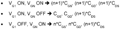
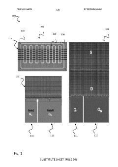
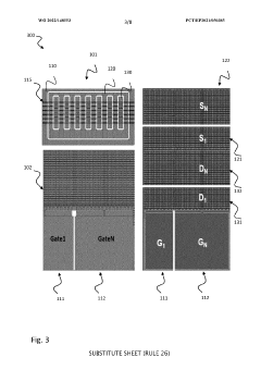
Multi-terminal gallium nitride power transistor
PatentWO2022148553A1
Innovation
- A configurable multi-terminal Gallium Nitride (GaN) power transistor with a split-gate design that allows for dynamic tuning of figures of merit during operation, enabling optimal efficiency at both light and heavy load conditions by modifying die area and performance through multiple gate, source, and drain terminals.
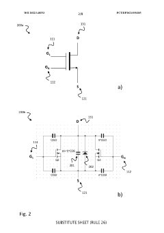
Devices and systems comprising drivers for power conversion circuits
PatentWO2014094115A1
Innovation
- A driver circuit with monitoring and control functions is introduced, utilizing a CMOS integrated circuit with a low voltage driver MOSFET, which includes latch and clamp circuitry to manage noise and transients, and an internal power source for self-powering, eliminating the need for a separate isolated power supply.


Thermal Management in Compact GaN Power Systems
Thermal management represents one of the most critical challenges in compact GaN power systems, directly impacting device reliability, performance, and lifespan. GaN devices generate significantly higher power densities compared to traditional silicon-based components, creating concentrated heat sources that require sophisticated cooling strategies. The superior electrical properties that enable miniaturization simultaneously intensify thermal stress, making effective heat dissipation essential for maintaining optimal power conversion efficiency.
The primary thermal challenge stems from GaN's inherently high power density capabilities, which can exceed 10 W/mm² in compact designs. This concentrated heat generation creates localized hot spots that can degrade device performance and trigger thermal runaway conditions. Junction temperatures exceeding 150°C significantly impact switching characteristics and long-term reliability, necessitating precise thermal control mechanisms.
Advanced thermal interface materials play a crucial role in compact GaN systems, with diamond-like carbon coatings and graphene-enhanced thermal pads offering thermal conductivities exceeding 400 W/mK. These materials facilitate efficient heat transfer from GaN dies to heat sinks while maintaining electrical isolation. Micro-channel cooling solutions have emerged as particularly effective, utilizing liquid coolants in precisely machined channels to achieve thermal resistances below 0.1 K/W.
Innovative packaging approaches address thermal constraints through multi-layer ceramic substrates and embedded cooling structures. Three-dimensional heat spreading techniques distribute thermal loads across larger surface areas, while integrated heat pipes and vapor chambers provide passive cooling solutions suitable for compact form factors. These approaches enable thermal management without compromising system miniaturization objectives.
Computational thermal modeling has become indispensable for optimizing compact GaN system designs, enabling prediction of temperature distributions and identification of thermal bottlenecks before physical prototyping. Advanced simulation tools incorporate electro-thermal coupling effects, allowing designers to optimize both electrical performance and thermal behavior simultaneously. This predictive capability accelerates development cycles and ensures thermal compliance in increasingly compact designs.
Safety Standards for High-Density GaN Power Designs
The rapid adoption of gallium nitride (GaN) technology in power conversion applications has necessitated the development of comprehensive safety standards specifically tailored for high-density power designs. As GaN devices enable unprecedented power densities and switching frequencies, traditional safety frameworks require significant adaptation to address the unique characteristics and potential hazards associated with these advanced semiconductor systems.
Current safety standards for GaN power designs primarily build upon existing frameworks such as IEC 60950-1, IEC 62368-1, and UL 1998, while incorporating specific provisions for wide bandgap semiconductor technologies. The International Electrotechnical Commission (IEC) has been actively developing supplementary guidelines that address the higher operating temperatures, faster switching transients, and increased electromagnetic interference potential inherent in GaN-based systems.
Thermal management represents a critical safety consideration in high-density GaN designs. Standards mandate specific junction temperature limits, typically not exceeding 150°C for commercial applications, along with requirements for thermal monitoring and protection circuits. The compact nature of GaN systems often results in concentrated heat generation, necessitating advanced thermal interface materials and heat dissipation strategies that comply with flammability ratings such as UL 94 V-0.
Electrical safety standards for GaN power systems emphasize isolation requirements, particularly given the high-frequency operation that can compromise traditional isolation barriers. Enhanced insulation coordination standards specify minimum creepage and clearance distances, accounting for the partial discharge characteristics unique to GaN switching behavior. Surge immunity requirements have been strengthened to address the sensitivity of GaN devices to voltage transients.
Electromagnetic compatibility (EMC) standards have evolved to accommodate the fast switching edges characteristic of GaN devices, which can generate significant conducted and radiated emissions. New measurement methodologies and limit specifications address frequencies extending well beyond traditional power electronics ranges, often requiring compliance up to several gigahertz.
Functional safety standards, particularly ISO 26262 for automotive applications and IEC 61508 for industrial systems, have incorporated specific failure mode analyses for GaN devices. These standards address the unique failure mechanisms of wide bandgap semiconductors, including gate oxide degradation and dynamic on-resistance drift, requiring enhanced diagnostic coverage and fault detection capabilities in safety-critical applications.
Unlock deeper insights with Patsnap Eureka Quick Research — get a full tech report to explore trends and direct your research. Try now!
Generate Your Research Report Instantly with AI Agent
Supercharge your innovation with Patsnap Eureka AI Agent Platform!