Disaggregated Memory vs SRAM: High-Throughput Workload Fit
MAY 12, 20269 MIN READ
Generate Your Research Report Instantly with AI Agent
PatSnap Eureka helps you evaluate technical feasibility & market potential.
Disaggregated Memory and SRAM Technology Background and Goals
Disaggregated memory and SRAM technologies represent two fundamentally different approaches to memory architecture design, each evolving along distinct trajectories to address the growing demands of high-throughput computing workloads. The historical development of these technologies reflects the continuous pursuit of balancing performance, scalability, and cost-effectiveness in modern data center environments.
SRAM technology has maintained its position as the gold standard for high-speed, low-latency memory applications since its inception in the 1960s. Its evolution has been characterized by consistent improvements in manufacturing processes, with transistor scaling enabling higher densities and faster access times. Modern SRAM implementations achieve sub-nanosecond access latencies and support extremely high bandwidth operations, making them indispensable for CPU caches, network processors, and real-time applications requiring deterministic performance characteristics.
Disaggregated memory emerged as a paradigm shift in the 2010s, driven by the limitations of traditional server-centric memory architectures. This approach decouples memory resources from compute nodes, enabling independent scaling and resource optimization across distributed systems. The technology leverages high-speed interconnects such as RDMA over InfiniBand or Ethernet to provide remote memory access with acceptable latency penalties compared to local memory access.
The primary technical goal of disaggregated memory systems is to achieve memory resource pooling and elastic scaling while maintaining performance levels suitable for production workloads. Current implementations target memory access latencies in the microsecond range, representing a significant improvement over traditional network storage but still orders of magnitude slower than local SRAM access.
SRAM technology continues to pursue aggressive scaling objectives, focusing on reducing power consumption per bit while increasing operational frequencies. Advanced SRAM designs incorporate techniques such as voltage scaling, process variation compensation, and novel cell topologies to maintain reliability at smaller geometries. The technology roadmap emphasizes achieving higher integration densities while preserving the fundamental advantage of zero refresh requirements and instant-on characteristics.
The convergence of these technologies in high-throughput workload scenarios presents unique opportunities for hybrid architectures. Emerging research explores tiered memory hierarchies that combine SRAM's ultra-low latency characteristics with disaggregated memory's scalability benefits, potentially enabling new classes of applications that require both high performance and massive memory capacity.
Market Demand for High-Throughput Computing Solutions
The global computing landscape is experiencing unprecedented demand for high-throughput solutions, driven by the exponential growth of data-intensive applications across multiple sectors. Cloud service providers, artificial intelligence companies, and scientific research institutions are increasingly seeking computing architectures that can handle massive parallel workloads while maintaining cost efficiency and energy optimization.
Enterprise applications such as real-time analytics, machine learning inference, and large-scale database operations require computing systems capable of processing terabytes of data with minimal latency. Traditional computing architectures face significant bottlenecks when dealing with memory-intensive workloads, creating substantial market opportunities for innovative memory solutions that can bridge the performance gap between processing units and storage systems.
The financial services sector demonstrates particularly strong demand for high-throughput computing, especially in algorithmic trading, risk modeling, and fraud detection systems. These applications require microsecond-level response times while processing millions of transactions simultaneously, pushing the boundaries of conventional memory hierarchies and creating urgent needs for more efficient memory architectures.
Scientific computing and research institutions represent another critical market segment, with applications in climate modeling, genomics research, and particle physics simulations requiring sustained high-throughput performance over extended periods. These workloads often involve complex data access patterns that challenge traditional memory systems, highlighting the importance of flexible and scalable memory solutions.
The emergence of edge computing and Internet of Things applications has further intensified demand for high-throughput solutions that can operate within constrained power and space requirements. This trend is driving innovation in memory technologies that can deliver superior performance per watt while maintaining the throughput characteristics required for real-time processing applications.
Market growth is also fueled by the increasing adoption of containerized applications and microservices architectures, which require computing infrastructure capable of rapidly scaling resources to meet fluctuating demand patterns. This dynamic environment necessitates memory solutions that can adapt quickly to varying workload characteristics while maintaining consistent high-throughput performance across diverse application scenarios.
Current State of Disaggregated Memory vs SRAM Technologies
The current landscape of disaggregated memory and SRAM technologies presents a complex ecosystem where traditional memory hierarchies are being challenged by emerging distributed architectures. Disaggregated memory systems have evolved from experimental concepts to production-ready solutions, with major cloud providers and enterprise vendors deploying these technologies at scale. Current implementations primarily focus on separating memory resources from compute nodes through high-speed interconnects, enabling dynamic memory allocation and improved resource utilization across data center environments.
SRAM technology continues to dominate high-performance computing scenarios where ultra-low latency and deterministic access patterns are critical. Modern SRAM implementations have achieved significant density improvements while maintaining sub-nanosecond access times, making them indispensable for cache hierarchies, network processing units, and real-time systems. However, SRAM faces fundamental scaling challenges due to manufacturing costs and power consumption constraints, particularly as workloads demand increasingly larger memory footprints.
The disaggregated memory ecosystem has matured considerably, with technologies like Intel Optane DC Persistent Memory, Samsung's CXL-enabled memory modules, and software-defined memory solutions from companies like MemVerge and ScaleFlux gaining commercial traction. These solutions typically achieve memory access latencies in the hundreds of nanoseconds to low microseconds range, representing a middle ground between traditional DRAM and storage-class memory.
Current technical barriers in disaggregated memory include network latency overhead, consistency protocols for distributed memory access, and application-level optimization requirements. Most implementations rely on RDMA-capable networks or emerging standards like Compute Express Link to minimize communication overhead. Software stack maturity remains a challenge, with limited operating system support and application frameworks specifically designed for disaggregated architectures.
SRAM technology faces different constraints, primarily centered around cost-per-bit economics and power density limitations. Advanced process nodes have enabled higher SRAM densities, but manufacturing yields and costs increase exponentially. Current SRAM solutions excel in scenarios requiring predictable performance characteristics but struggle with workloads demanding large memory capacities due to prohibitive costs and power requirements.
The geographical distribution of these technologies shows concentration in major semiconductor manufacturing regions, with leading-edge SRAM production primarily in Taiwan, South Korea, and advanced fabs in the United States. Disaggregated memory innovation centers around major cloud providers' research facilities and memory-focused startups in Silicon Valley, with significant development activities in China and Europe focusing on alternative memory architectures and interconnect technologies.
Existing Memory Solutions for High-Throughput Workloads
01 Disaggregated memory architecture and management
Systems and methods for implementing disaggregated memory architectures that separate memory resources from compute resources, allowing for flexible allocation and management of memory across distributed computing environments. These approaches enable dynamic memory provisioning and improved resource utilization through centralized memory pools that can be accessed by multiple processing units.- Disaggregated memory architecture and management: Systems and methods for implementing disaggregated memory architectures that separate memory resources from compute resources, allowing for flexible allocation and management of memory across distributed computing environments. These approaches enable dynamic memory provisioning and improved resource utilization through centralized memory pools that can be accessed by multiple compute nodes.
- SRAM throughput optimization techniques: Methods for enhancing SRAM performance through various optimization strategies including advanced access patterns, pipelining techniques, and bandwidth management. These solutions focus on maximizing data transfer rates and minimizing latency in SRAM operations through improved circuit design and access scheduling algorithms.
- Memory controller and interface optimization: Advanced memory controller designs and interface protocols that improve data throughput between processors and memory systems. These technologies include sophisticated buffering mechanisms, command queuing strategies, and protocol optimizations that reduce memory access latency while increasing overall system performance.
- Cache hierarchy and memory subsystem integration: Integrated approaches for optimizing cache hierarchies and memory subsystems to improve overall memory throughput. These solutions involve coordinated management of different memory levels, intelligent prefetching mechanisms, and adaptive caching strategies that enhance data availability and reduce memory bottlenecks.
- High-performance memory interconnect and networking: Technologies for implementing high-speed interconnects and networking solutions that enable efficient communication between disaggregated memory components and computing resources. These systems provide low-latency, high-bandwidth connections that support scalable memory architectures and distributed computing environments.
02 SRAM throughput optimization techniques
Methods for enhancing static random-access memory throughput through various optimization strategies including advanced access patterns, pipelining techniques, and bandwidth management. These solutions focus on maximizing data transfer rates and minimizing latency in SRAM operations to improve overall system performance.Expand Specific Solutions03 Memory controller and interface enhancements
Advanced memory controller designs and interface protocols that facilitate high-speed communication between processing units and disaggregated memory systems. These innovations include specialized controllers that manage memory access requests, optimize data flow, and maintain coherency across distributed memory architectures.Expand Specific Solutions04 Cache coherency and synchronization mechanisms
Techniques for maintaining data consistency and synchronization in disaggregated memory systems, particularly focusing on cache coherency protocols and synchronization primitives. These methods ensure data integrity when multiple processors access shared memory resources in distributed computing environments.Expand Specific Solutions05 Performance monitoring and adaptive memory allocation
Systems for monitoring memory performance metrics and implementing adaptive allocation strategies in disaggregated memory environments. These solutions include real-time performance analysis, dynamic resource allocation algorithms, and intelligent memory management policies that optimize throughput based on workload characteristics.Expand Specific Solutions
Key Players in Memory and High-Performance Computing Industry
The disaggregated memory versus SRAM competition for high-throughput workloads represents a rapidly evolving market at a critical inflection point. The industry is transitioning from early adoption to mainstream deployment, driven by increasing demand for memory-intensive applications and AI workloads. Market growth is accelerating as enterprises seek cost-effective alternatives to traditional SRAM architectures. Technology maturity varies significantly across players, with established semiconductor leaders like Samsung Electronics, Micron Technology, and Intel driving innovation through advanced memory architectures and manufacturing capabilities. Memory specialists such as ChangXin Memory Technologies and emerging players like Taalas are developing specialized solutions, while system integrators including Google, Huawei, and IBM are implementing these technologies in large-scale deployments. The competitive landscape shows strong momentum toward disaggregated memory solutions, particularly for cloud and data center applications where throughput requirements exceed traditional SRAM limitations.
Samsung Electronics Co., Ltd.
Technical Solution: Samsung has developed High Bandwidth Memory (HBM) and Processing-in-Memory (PIM) technologies to address high-throughput workload requirements. Their approach integrates SRAM-based buffer memory with HBM stacks, enabling near-data computing capabilities. Samsung's disaggregated memory solution utilizes their AQUABOLT HBM2E with up to 460GB/s bandwidth per stack, combined with intelligent memory controllers that can dynamically partition memory resources across multiple compute nodes. The company's PIM technology reduces data movement by performing computations directly within the memory subsystem, particularly beneficial for AI and machine learning workloads requiring massive parallel processing.
Strengths: Industry-leading memory bandwidth, proven HBM manufacturing capabilities, innovative PIM technology for reduced data movement. Weaknesses: Higher cost per bit compared to traditional DRAM, limited software ecosystem for PIM programming models.
Google LLC
Technical Solution: Google has implemented disaggregated memory architectures in their data centers through custom silicon solutions and software-defined memory management. Their approach leverages Tensor Processing Units (TPUs) with large on-chip SRAM buffers combined with remote memory pools accessible via high-speed interconnects. Google's system dynamically balances between local SRAM for latency-critical operations and disaggregated memory for capacity-intensive workloads. Their software stack includes intelligent memory placement algorithms that predict access patterns and pre-position data accordingly. The company reports achieving 2-3x improvement in memory utilization efficiency while maintaining sub-microsecond access times for frequently used data through their hybrid SRAM-disaggregated memory hierarchy.
Strengths: Massive scale deployment experience, custom silicon optimization, advanced ML-driven memory management algorithms. Weaknesses: Proprietary solutions with limited commercial availability, requires significant infrastructure investment for implementation.
Core Innovations in Disaggregated Memory Technologies
Static random-access memory (SRAM) cell for high-speed content-addressable memory and in-memory boolean logic operation
PatentInactiveUS20230197154A1
Innovation
- An 8T SRAM cell is proposed, incorporating two additional PMOS access transistors with differential read ports, which reduces read disturbance by using PMOS transistors for access and precharging the read bit line to ground, enabling high-speed and stable IMC operations.


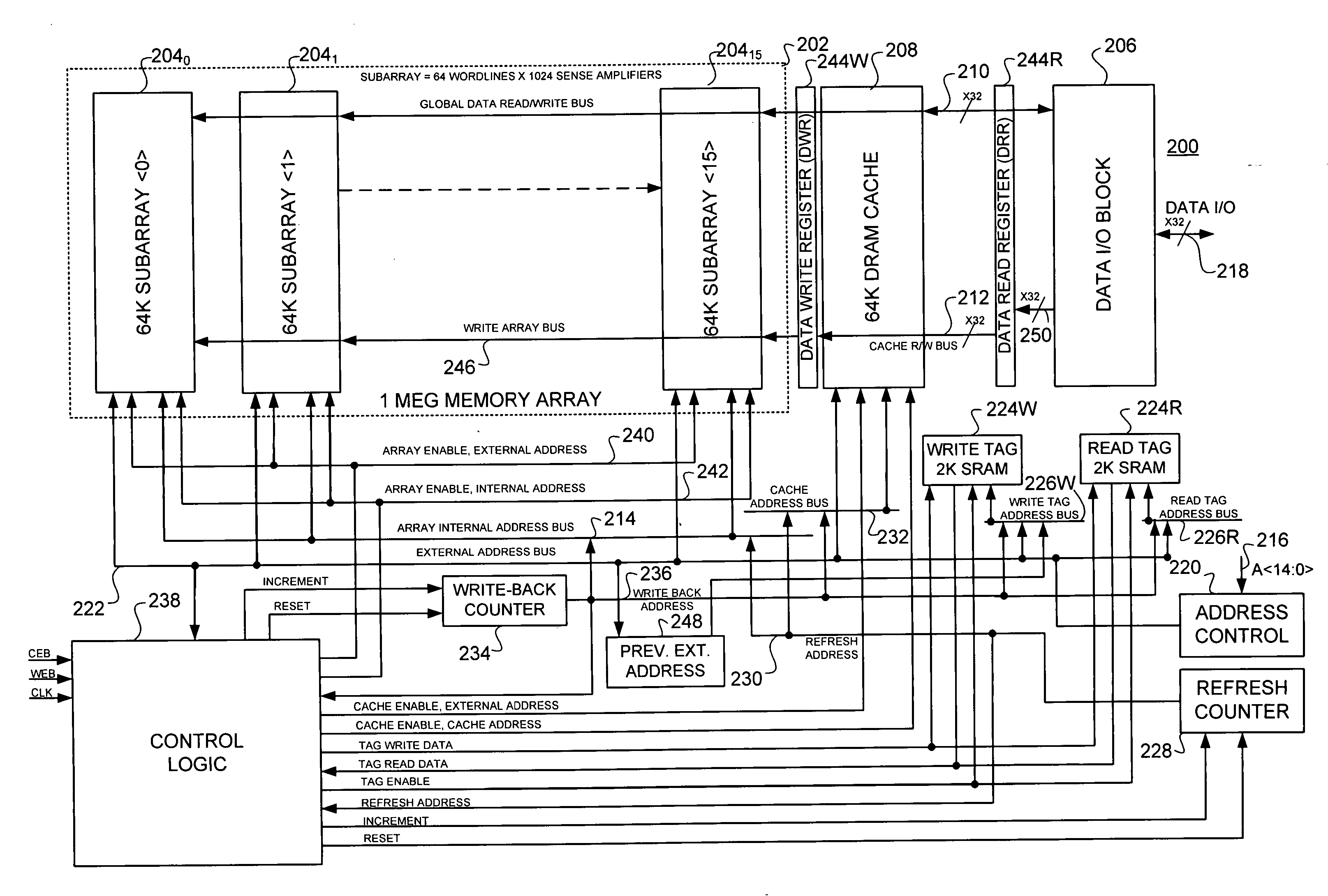
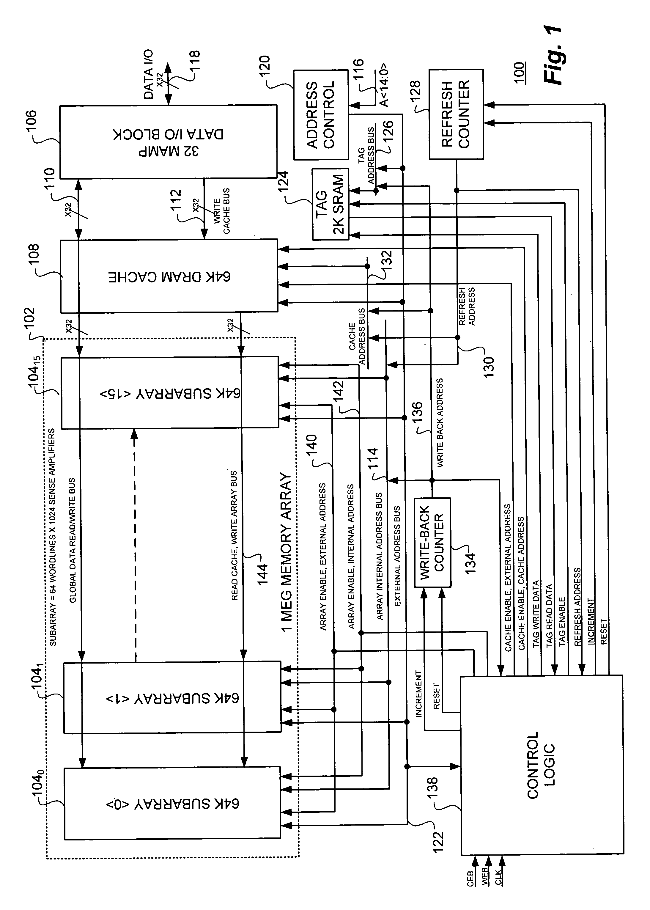
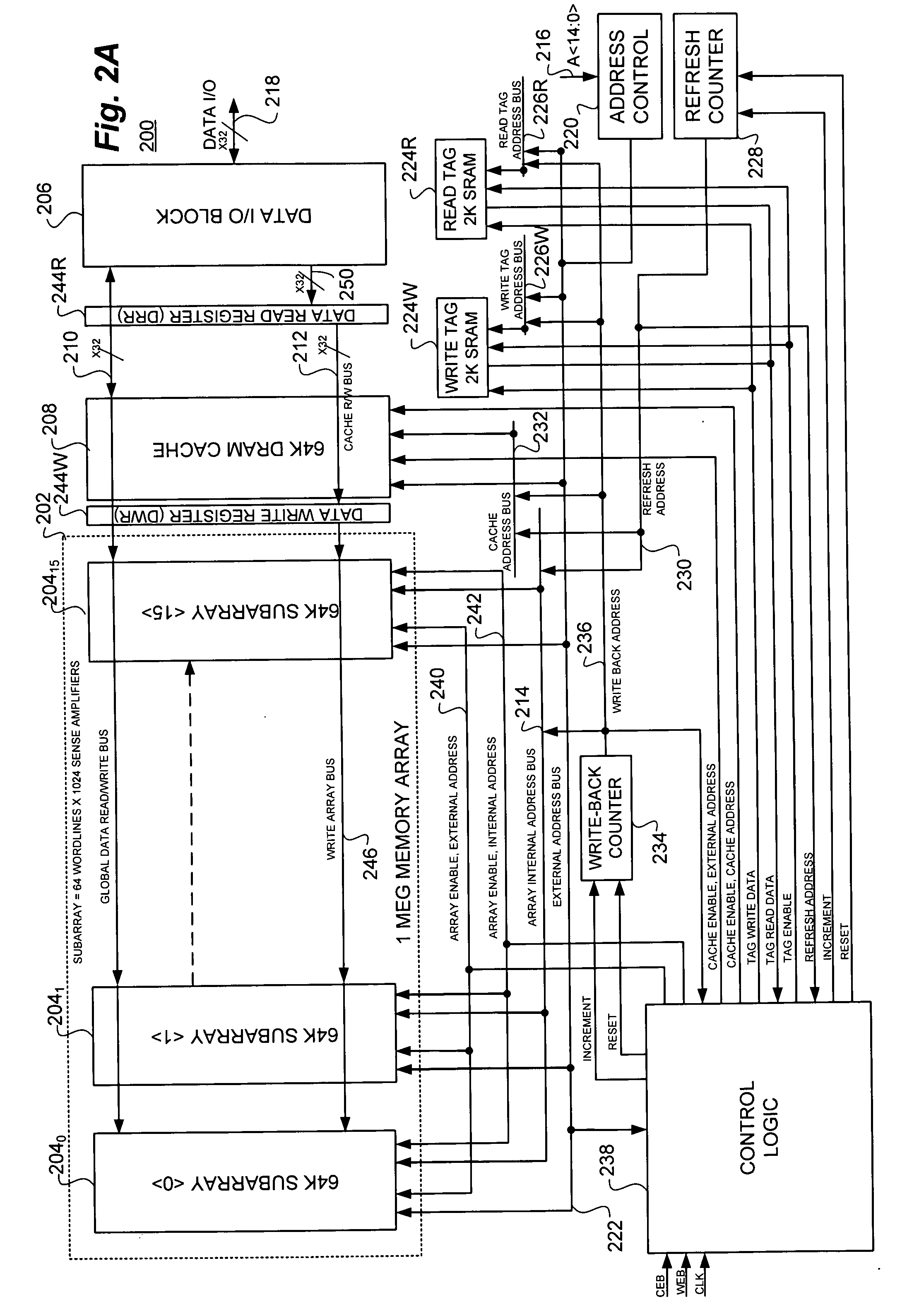
Static random access memory (SRAM) compatible, high availability memory array and method employing synchronous dynamic random access memory (DRAM) in conjunction with a data cache and separate read and write registers and tag blocks
PatentInactiveUS20060190676A1
Innovation
- A high-speed, static random access memory (SRAM) compatible memory array is developed, employing synchronous dynamic random access memory (DRAM) with a single DRAM cache and separate read and write data registers, along with dual tags to manage cache operations efficiently, thereby reducing cycle time and power consumption.

Performance Benchmarking and Evaluation Methodologies
Establishing comprehensive performance benchmarking methodologies for disaggregated memory versus SRAM in high-throughput workloads requires a multi-dimensional evaluation framework. The primary challenge lies in developing metrics that accurately capture the nuanced performance characteristics of both memory architectures under varying computational demands. Traditional benchmarking approaches often fail to account for the distributed nature of disaggregated memory systems and their inherent latency variations.
The evaluation methodology must incorporate both synthetic and real-world workload patterns to ensure comprehensive assessment. Synthetic benchmarks should focus on memory access patterns, bandwidth utilization, and latency sensitivity measurements. These controlled tests enable precise isolation of performance variables and facilitate direct comparison between SRAM and disaggregated memory configurations. Key synthetic metrics include sequential and random access throughput, memory bandwidth saturation points, and latency distribution analysis under different load conditions.
Real-world workload evaluation presents additional complexity due to the heterogeneous nature of high-throughput applications. Database operations, machine learning inference, and streaming analytics each exhibit distinct memory access patterns that significantly impact performance outcomes. The benchmarking framework must capture application-specific metrics such as transaction processing rates, model inference latency, and data pipeline throughput to provide actionable insights for system architects.
Standardized testing environments are crucial for ensuring reproducible and comparable results across different hardware configurations. The methodology should define specific hardware specifications, network configurations, and software stack requirements to minimize environmental variables. Additionally, the framework must account for thermal throttling, power consumption variations, and system stability under sustained high-throughput operations.
Statistical analysis methodologies play a critical role in interpreting benchmark results and identifying performance trends. The evaluation framework should incorporate confidence intervals, percentile analysis, and regression modeling to quantify performance differences and predict scaling behavior. This analytical approach enables decision-makers to assess the statistical significance of performance variations and make informed architectural choices based on empirical evidence rather than theoretical assumptions.
Cost-Benefit Analysis of Memory Architecture Choices
The economic evaluation of disaggregated memory versus SRAM architectures for high-throughput workloads reveals significant cost differentials across multiple dimensions. Initial capital expenditure analysis demonstrates that SRAM-based solutions require substantially higher upfront investment, with costs ranging from $8-15 per gigabyte compared to disaggregated memory's $2-4 per gigabyte. However, this comparison becomes more nuanced when factoring in infrastructure requirements and deployment complexity.
Operational expenditure patterns show contrasting profiles between the two architectures. SRAM systems exhibit lower power consumption per access operation, typically consuming 0.1-0.5 picojoules per bit, while disaggregated memory solutions consume 10-50 picojoules per bit due to network traversal overhead. For high-frequency trading and real-time analytics workloads processing millions of transactions per second, this power differential translates to significant operational cost variations over multi-year deployment cycles.
Total cost of ownership calculations must incorporate scalability economics and maintenance overhead. Disaggregated memory architectures demonstrate superior cost scaling characteristics, with linear cost growth as memory requirements expand. SRAM solutions face exponential cost increases beyond certain capacity thresholds due to physical constraints and cooling requirements. The break-even point typically occurs at 512GB-1TB memory pool sizes for sustained high-throughput operations.
Performance-adjusted cost metrics reveal that while SRAM delivers 10-100x lower latency, the cost per transaction processed favors disaggregated memory for workloads exceeding 100,000 operations per second with moderate latency tolerance. Financial modeling indicates that disaggregated architectures achieve 40-60% lower five-year total cost of ownership for large-scale deployments, despite higher per-operation latency penalties.
Risk-adjusted return calculations must account for technology obsolescence cycles and upgrade flexibility. Disaggregated memory systems offer superior investment protection through modular scaling and technology refresh capabilities, while SRAM investments face higher stranding risks due to integrated hardware dependencies and limited upgrade pathways.
Unlock deeper insights with PatSnap Eureka Quick Research — get a full tech report to explore trends and direct your research. Try now!
Generate Your Research Report Instantly with AI Agent
Supercharge your innovation with PatSnap Eureka AI Agent Platform!