
Enhancing Circuit Performance with Schottky Diode Arrays
MAR 24, 20269 MIN READ
Generate Your Research Report Instantly with AI Agent
Patsnap Eureka helps you evaluate technical feasibility & market potential.
Schottky Diode Array Circuit Enhancement Background and Objectives
Schottky diode arrays have emerged as critical components in modern electronic systems, driven by the increasing demand for high-frequency, low-power, and high-efficiency circuit designs. The evolution of semiconductor technology has positioned these devices at the forefront of addressing performance bottlenecks in various applications, from radio frequency circuits to power management systems. The unique characteristics of Schottky diodes, including their low forward voltage drop and fast switching capabilities, make them particularly valuable when configured in array architectures.
The historical development of Schottky diode technology traces back to the 1930s when Walter Schottky first described the metal-semiconductor junction phenomenon. However, practical implementation in array configurations gained momentum in the 1980s with advances in semiconductor fabrication processes. The transition from discrete components to integrated array structures marked a significant milestone, enabling designers to achieve superior circuit performance through optimized layout geometries and enhanced thermal management.
Contemporary circuit design challenges have intensified the focus on Schottky diode arrays as enabling technologies. The proliferation of wireless communication systems, Internet of Things devices, and electric vehicle applications has created unprecedented demands for components that can operate efficiently across wide frequency ranges while maintaining minimal power consumption. Traditional silicon diodes often fall short in meeting these stringent requirements, particularly in high-frequency switching applications where parasitic capacitances and reverse recovery times become limiting factors.
The primary objective of enhancing circuit performance through Schottky diode arrays centers on achieving optimal trade-offs between speed, efficiency, and reliability. Key performance metrics include reducing switching losses, minimizing electromagnetic interference, improving thermal dissipation, and enhancing overall system reliability. These objectives align with broader industry trends toward miniaturization and energy efficiency, where every component must contribute to overall system optimization.
Array configurations offer unique advantages over single-diode implementations by enabling parallel processing capabilities, redundancy for improved reliability, and distributed thermal management. The geometric arrangement of diodes within arrays can be tailored to specific application requirements, whether for voltage multiplication, signal rectification, or protection circuits. This flexibility represents a fundamental shift from traditional discrete component approaches toward integrated solutions that maximize performance density.
The technological evolution continues to push boundaries in materials science, with silicon carbide and gallium arsenide substrates offering superior performance characteristics compared to conventional silicon. These advanced materials enable Schottky diode arrays to operate at higher temperatures, frequencies, and power levels, expanding their applicability across demanding industrial and aerospace applications.
The historical development of Schottky diode technology traces back to the 1930s when Walter Schottky first described the metal-semiconductor junction phenomenon. However, practical implementation in array configurations gained momentum in the 1980s with advances in semiconductor fabrication processes. The transition from discrete components to integrated array structures marked a significant milestone, enabling designers to achieve superior circuit performance through optimized layout geometries and enhanced thermal management.
Contemporary circuit design challenges have intensified the focus on Schottky diode arrays as enabling technologies. The proliferation of wireless communication systems, Internet of Things devices, and electric vehicle applications has created unprecedented demands for components that can operate efficiently across wide frequency ranges while maintaining minimal power consumption. Traditional silicon diodes often fall short in meeting these stringent requirements, particularly in high-frequency switching applications where parasitic capacitances and reverse recovery times become limiting factors.
The primary objective of enhancing circuit performance through Schottky diode arrays centers on achieving optimal trade-offs between speed, efficiency, and reliability. Key performance metrics include reducing switching losses, minimizing electromagnetic interference, improving thermal dissipation, and enhancing overall system reliability. These objectives align with broader industry trends toward miniaturization and energy efficiency, where every component must contribute to overall system optimization.
Array configurations offer unique advantages over single-diode implementations by enabling parallel processing capabilities, redundancy for improved reliability, and distributed thermal management. The geometric arrangement of diodes within arrays can be tailored to specific application requirements, whether for voltage multiplication, signal rectification, or protection circuits. This flexibility represents a fundamental shift from traditional discrete component approaches toward integrated solutions that maximize performance density.
The technological evolution continues to push boundaries in materials science, with silicon carbide and gallium arsenide substrates offering superior performance characteristics compared to conventional silicon. These advanced materials enable Schottky diode arrays to operate at higher temperatures, frequencies, and power levels, expanding their applicability across demanding industrial and aerospace applications.
Market Demand for High-Performance Schottky Diode Solutions
The global semiconductor market continues to experience unprecedented growth, driven by the proliferation of electronic devices across consumer, automotive, industrial, and telecommunications sectors. Within this expanding landscape, high-performance Schottky diode solutions have emerged as critical components for next-generation circuit designs that demand superior efficiency, speed, and reliability.
Power management applications represent the largest segment driving demand for advanced Schottky diode arrays. Modern electronic systems require increasingly sophisticated power conversion and regulation capabilities to support high-performance processors, memory modules, and specialized integrated circuits. The transition toward higher switching frequencies in power supplies necessitates diodes with minimal forward voltage drop and ultra-fast recovery times, characteristics that Schottky diodes inherently provide.
The automotive industry has become a significant growth driver, particularly with the accelerated adoption of electric vehicles and advanced driver assistance systems. These applications demand robust semiconductor solutions capable of operating under extreme conditions while maintaining high efficiency. Schottky diode arrays play crucial roles in battery management systems, DC-DC converters, and motor control circuits where energy efficiency directly impacts vehicle performance and range.
Telecommunications infrastructure modernization, including the deployment of fifth-generation wireless networks, creates substantial demand for high-frequency switching components. Base stations, network equipment, and data centers require power management solutions that can handle increased data throughput while minimizing energy consumption. Schottky diodes excel in these applications due to their superior high-frequency characteristics and thermal stability.
Consumer electronics manufacturers increasingly prioritize compact, energy-efficient designs to meet market expectations for longer battery life and reduced form factors. Portable devices, wearables, and Internet of Things applications drive demand for miniaturized Schottky diode solutions that maintain performance while occupying minimal board space.
Industrial automation and renewable energy sectors present emerging opportunities for specialized Schottky diode applications. Solar inverters, wind power systems, and industrial motor drives require components that can withstand harsh operating environments while delivering consistent performance over extended operational lifespans.
Market dynamics indicate strong preference for integrated solutions that combine multiple diodes within single packages, enabling simplified circuit designs and improved thermal management. This trend toward integration aligns with broader industry movements toward system-level optimization and cost reduction through component consolidation.
Power management applications represent the largest segment driving demand for advanced Schottky diode arrays. Modern electronic systems require increasingly sophisticated power conversion and regulation capabilities to support high-performance processors, memory modules, and specialized integrated circuits. The transition toward higher switching frequencies in power supplies necessitates diodes with minimal forward voltage drop and ultra-fast recovery times, characteristics that Schottky diodes inherently provide.
The automotive industry has become a significant growth driver, particularly with the accelerated adoption of electric vehicles and advanced driver assistance systems. These applications demand robust semiconductor solutions capable of operating under extreme conditions while maintaining high efficiency. Schottky diode arrays play crucial roles in battery management systems, DC-DC converters, and motor control circuits where energy efficiency directly impacts vehicle performance and range.
Telecommunications infrastructure modernization, including the deployment of fifth-generation wireless networks, creates substantial demand for high-frequency switching components. Base stations, network equipment, and data centers require power management solutions that can handle increased data throughput while minimizing energy consumption. Schottky diodes excel in these applications due to their superior high-frequency characteristics and thermal stability.
Consumer electronics manufacturers increasingly prioritize compact, energy-efficient designs to meet market expectations for longer battery life and reduced form factors. Portable devices, wearables, and Internet of Things applications drive demand for miniaturized Schottky diode solutions that maintain performance while occupying minimal board space.
Industrial automation and renewable energy sectors present emerging opportunities for specialized Schottky diode applications. Solar inverters, wind power systems, and industrial motor drives require components that can withstand harsh operating environments while delivering consistent performance over extended operational lifespans.
Market dynamics indicate strong preference for integrated solutions that combine multiple diodes within single packages, enabling simplified circuit designs and improved thermal management. This trend toward integration aligns with broader industry movements toward system-level optimization and cost reduction through component consolidation.
Current State and Challenges of Schottky Diode Array Technology
Schottky diode array technology has reached a mature stage in terms of fundamental device physics and manufacturing processes, yet significant challenges persist in optimizing performance for advanced circuit applications. Current fabrication techniques primarily rely on metal-semiconductor junction formation using materials such as platinum silicide, titanium silicide, and various compound semiconductors including gallium arsenide and silicon carbide substrates.
The state-of-the-art manufacturing processes have achieved remarkable precision in controlling barrier heights, typically ranging from 0.3 to 1.2 eV depending on the metal-semiconductor combination. Modern photolithography and etching techniques enable array densities exceeding 10^6 diodes per square centimeter, with individual diode dimensions scaling down to sub-micron levels. However, process uniformity across large wafer areas remains a critical limitation, with barrier height variations of ±50 mV commonly observed.
Temperature stability represents one of the most pressing challenges in current Schottky diode array implementations. The inherent temperature coefficient of barrier height, typically -2 mV/°C, causes significant performance drift in precision applications. This thermal sensitivity becomes particularly problematic in high-power circuits where self-heating effects compound the issue, leading to thermal runaway conditions in poorly designed arrays.
Parasitic effects constitute another major challenge limiting circuit performance enhancement. Inter-diode coupling through substrate resistance and capacitance creates unwanted signal crosstalk, especially in high-frequency applications above 10 GHz. The distributed nature of array parasitics makes circuit modeling complex and often inaccurate, hindering optimal design implementation.
Reliability concerns persist despite decades of development, particularly regarding electromigration in metal contacts and interface degradation under high current density conditions. Current density limitations typically restrict operation to below 10^5 A/cm², constraining the power handling capabilities of compact array designs.
Manufacturing cost remains elevated due to the precision required in metal deposition and pattern definition processes. The need for specialized equipment and clean room facilities limits widespread adoption, particularly in cost-sensitive consumer applications where silicon PN junction alternatives remain more economically viable.
The state-of-the-art manufacturing processes have achieved remarkable precision in controlling barrier heights, typically ranging from 0.3 to 1.2 eV depending on the metal-semiconductor combination. Modern photolithography and etching techniques enable array densities exceeding 10^6 diodes per square centimeter, with individual diode dimensions scaling down to sub-micron levels. However, process uniformity across large wafer areas remains a critical limitation, with barrier height variations of ±50 mV commonly observed.
Temperature stability represents one of the most pressing challenges in current Schottky diode array implementations. The inherent temperature coefficient of barrier height, typically -2 mV/°C, causes significant performance drift in precision applications. This thermal sensitivity becomes particularly problematic in high-power circuits where self-heating effects compound the issue, leading to thermal runaway conditions in poorly designed arrays.
Parasitic effects constitute another major challenge limiting circuit performance enhancement. Inter-diode coupling through substrate resistance and capacitance creates unwanted signal crosstalk, especially in high-frequency applications above 10 GHz. The distributed nature of array parasitics makes circuit modeling complex and often inaccurate, hindering optimal design implementation.
Reliability concerns persist despite decades of development, particularly regarding electromigration in metal contacts and interface degradation under high current density conditions. Current density limitations typically restrict operation to below 10^5 A/cm², constraining the power handling capabilities of compact array designs.
Manufacturing cost remains elevated due to the precision required in metal deposition and pattern definition processes. The need for specialized equipment and clean room facilities limits widespread adoption, particularly in cost-sensitive consumer applications where silicon PN junction alternatives remain more economically viable.
Existing Circuit Performance Enhancement Solutions
01 Schottky diode array structure and layout optimization
Optimizing the physical structure and layout of Schottky diode arrays can significantly improve circuit performance. This includes arrangements of multiple diodes in specific configurations, spacing optimization between diode elements, and geometric design considerations to minimize parasitic effects. The structural design affects key parameters such as capacitance, resistance, and switching characteristics of the array.- Schottky diode array structure and layout optimization: The physical arrangement and structural design of Schottky diodes in array configurations significantly impacts circuit performance. Optimized layouts can reduce parasitic capacitance and resistance, improve thermal management, and enhance overall electrical characteristics. Various geometric configurations and spacing arrangements between individual diodes in the array are employed to achieve better performance metrics such as switching speed and power handling capability.
- Integration of Schottky diode arrays with semiconductor devices: Schottky diode arrays can be integrated with other semiconductor components to form complex circuits with enhanced functionality. This integration approach allows for improved circuit density, reduced interconnection losses, and better overall system performance. The co-fabrication techniques enable the creation of monolithic structures that combine the fast switching characteristics of Schottky diodes with other active and passive components on the same substrate.
- Thermal management and heat dissipation in Schottky diode arrays: Effective thermal management is critical for maintaining optimal performance in Schottky diode arrays, especially in high-power applications. Various heat dissipation structures and thermal coupling techniques are employed to prevent performance degradation due to elevated temperatures. Advanced packaging methods and substrate materials with high thermal conductivity help distribute heat more evenly across the array, ensuring consistent electrical characteristics and extended device lifetime.
- Voltage clamping and protection circuits using Schottky diode arrays: Schottky diode arrays are utilized in voltage clamping and circuit protection applications to safeguard sensitive electronic components from overvoltage conditions. The low forward voltage drop and fast switching characteristics of Schottky diodes make them ideal for transient voltage suppression. Array configurations provide multiple protection paths and can be designed to handle various voltage levels and current requirements in different circuit topologies.
- High-frequency and switching performance enhancement: Schottky diode arrays are specifically designed to achieve superior high-frequency operation and fast switching performance in various circuit applications. The inherent low junction capacitance and absence of minority carrier storage enable rapid transitions between conducting and non-conducting states. Design techniques focus on minimizing parasitic elements and optimizing the metal-semiconductor interface to achieve maximum switching speeds and efficiency in RF circuits, power converters, and high-speed digital applications.
02 Integration of Schottky diodes with semiconductor devices
Integrating Schottky diode arrays with other semiconductor components such as transistors, MOSFETs, or integrated circuits enhances overall circuit performance. This integration approach improves switching speed, reduces power consumption, and enables compact circuit designs. The monolithic integration techniques allow for better thermal management and reduced interconnection losses.Expand Specific Solutions03 High-frequency and high-speed switching applications
Schottky diode arrays are specifically designed and optimized for high-frequency and high-speed switching applications. The low forward voltage drop and fast recovery time characteristics make them suitable for RF circuits, power converters, and high-speed digital applications. Design considerations include minimizing junction capacitance and optimizing carrier mobility for enhanced switching performance.Expand Specific Solutions04 Thermal management and power handling in diode arrays
Effective thermal management techniques are crucial for maintaining performance and reliability of Schottky diode arrays under high power conditions. This includes heat dissipation structures, thermal coupling considerations, and temperature-dependent performance optimization. Proper thermal design prevents performance degradation and extends device lifetime in power electronics applications.Expand Specific Solutions05 Protection and ESD circuits using Schottky diode arrays
Schottky diode arrays are employed in protection circuits and electrostatic discharge applications to safeguard sensitive electronic components. The arrays provide clamping functions, voltage regulation, and transient suppression capabilities. Design strategies focus on achieving low clamping voltage, high current handling capability, and fast response time to protect against voltage spikes and ESD events.Expand Specific Solutions
Key Players in Schottky Diode and Semiconductor Industry
The Schottky diode array market represents a mature yet evolving segment within the broader semiconductor industry, currently valued at several billion dollars with steady growth driven by automotive, telecommunications, and power management applications. The industry demonstrates advanced technological maturity, with established players like Taiwan Semiconductor Manufacturing Co., Infineon Technologies, and ROHM Co. leading in manufacturing capabilities and process innovations. Key competitors including ON Semiconductor, Power Integrations, and Wolfspeed are driving technological advancement through specialized high-performance solutions, while Asian manufacturers such as SMIC and Shanghai Huahong Grace provide cost-effective alternatives. The competitive landscape shows consolidation among tier-one suppliers, with companies like Toshiba Electronic Devices, Mitsubishi Electric, and Microchip Technology leveraging integrated design and manufacturing capabilities to maintain market position in this technology-intensive sector.
Infineon Technologies AG
Technical Solution: Infineon develops advanced Schottky diode arrays with silicon carbide (SiC) technology, featuring ultra-low forward voltage drop of 0.3V and reverse recovery times under 25ns. Their CoolSiC Schottky diodes integrate multiple diodes in single packages for power factor correction and switching applications. The company's proprietary trench MOS barrier technology reduces leakage current by 90% while maintaining fast switching characteristics. These arrays support frequencies up to 1MHz with junction temperatures reaching 175°C, making them suitable for automotive and industrial power systems.
Strengths: Industry-leading SiC technology with excellent thermal performance and low switching losses. Weaknesses: Higher cost compared to silicon alternatives and limited availability in high-volume applications.
ROHM Co., Ltd.
Technical Solution: ROHM develops compact Schottky diode arrays using advanced silicon and SiC technologies for automotive and consumer electronics. Their arrays feature forward voltage drops of 0.4V and reverse leakage currents below 10μA at 25°C. The company's proprietary guard ring structure enhances breakdown voltage reliability while reducing chip size by 30%. Multi-diode configurations in single packages support current ratings from 1A to 30A with operating frequencies up to 500kHz. ROHM's arrays incorporate thermal coupling optimization to prevent hot-spot formation and ensure uniform current distribution across multiple diodes.
Strengths: Excellent miniaturization capabilities and reliable automotive-grade quality standards. Weaknesses: Limited high-power applications and moderate switching speed compared to pure SiC solutions.
Core Innovations in Schottky Diode Array Design
Schottky Diodes Having Low-Voltage and High-Concentration Rings
PatentInactiveUS20090294865A1
Innovation
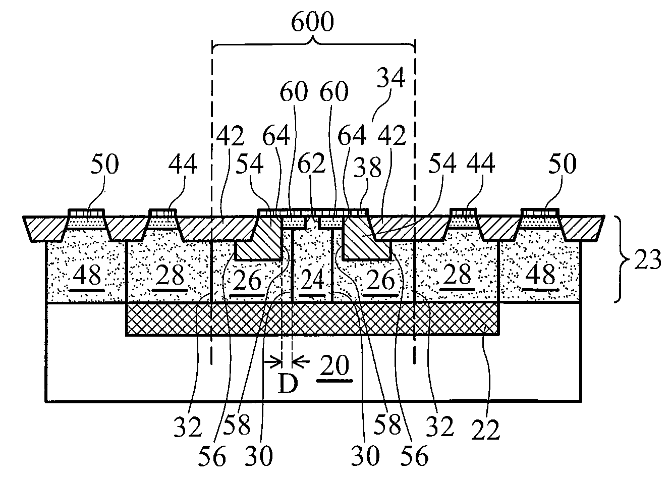
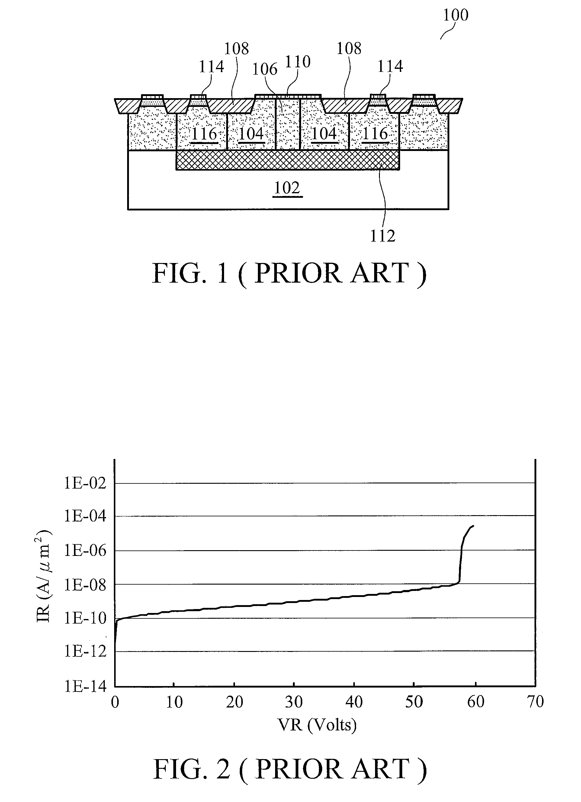
- The structure includes a semiconductor substrate with high-voltage n-type and p-type well regions, a metal-containing layer forming a Schottky barrier, a low-voltage p-type well region, and a heavily doped p-type region, which reduces leakage current and increases on-current by modifying the Schottky diode design with additional fingers connected in parallel.

Schottky diode employing recesses for elements of junction barrier array
PatentWO2013036724A1
Innovation
- A Schottky diode design featuring a substrate with a drift layer and a Schottky layer, incorporating a junction barrier array with doped regions and recesses to enhance the depth of these regions, along with edge termination structures like guard rings and a mesa guard ring, formed using ion implantation to improve electric field suppression and current/voltage characteristics.


Thermal Management Strategies for Schottky Arrays
Thermal management represents one of the most critical challenges in implementing high-performance Schottky diode arrays, as these devices generate substantial heat during operation that can severely impact their electrical characteristics and long-term reliability. The inherently low forward voltage drop that makes Schottky diodes attractive for high-frequency applications also results in concentrated power dissipation, particularly in array configurations where multiple devices operate simultaneously within confined spaces.
Effective heat dissipation strategies begin with optimized substrate selection and thermal interface materials. Silicon carbide and gallium nitride substrates offer superior thermal conductivity compared to traditional silicon, enabling more efficient heat transfer from the active junction to the package. Advanced thermal interface materials, including diamond-like carbon coatings and high-conductivity metal matrix composites, provide enhanced thermal pathways while maintaining electrical isolation where required.
Package-level thermal management employs sophisticated heat sink designs and thermal spreading techniques. Copper-based heat spreaders with optimized fin geometries maximize surface area for convective cooling, while embedded heat pipes and vapor chambers enable rapid heat transport away from hotspots. For high-power array applications, liquid cooling systems with microchannel heat exchangers provide superior thermal performance, though at increased system complexity.
Array-level thermal considerations focus on minimizing thermal coupling between adjacent devices and managing temperature gradients across the array. Strategic device spacing, thermal isolation trenches, and differential heat sinking help prevent thermal runaway conditions where localized heating degrades neighboring devices. Temperature-aware circuit design techniques, including thermal feedback control and dynamic load balancing, actively manage power distribution to maintain uniform temperature profiles.
Advanced thermal management approaches incorporate real-time temperature monitoring and adaptive control systems. Integrated temperature sensors enable precise thermal mapping across the array, while intelligent power management algorithms dynamically adjust operating parameters to prevent thermal stress. These systems balance performance optimization with thermal constraints, ensuring reliable operation across varying environmental conditions and load profiles.
Effective heat dissipation strategies begin with optimized substrate selection and thermal interface materials. Silicon carbide and gallium nitride substrates offer superior thermal conductivity compared to traditional silicon, enabling more efficient heat transfer from the active junction to the package. Advanced thermal interface materials, including diamond-like carbon coatings and high-conductivity metal matrix composites, provide enhanced thermal pathways while maintaining electrical isolation where required.
Package-level thermal management employs sophisticated heat sink designs and thermal spreading techniques. Copper-based heat spreaders with optimized fin geometries maximize surface area for convective cooling, while embedded heat pipes and vapor chambers enable rapid heat transport away from hotspots. For high-power array applications, liquid cooling systems with microchannel heat exchangers provide superior thermal performance, though at increased system complexity.
Array-level thermal considerations focus on minimizing thermal coupling between adjacent devices and managing temperature gradients across the array. Strategic device spacing, thermal isolation trenches, and differential heat sinking help prevent thermal runaway conditions where localized heating degrades neighboring devices. Temperature-aware circuit design techniques, including thermal feedback control and dynamic load balancing, actively manage power distribution to maintain uniform temperature profiles.
Advanced thermal management approaches incorporate real-time temperature monitoring and adaptive control systems. Integrated temperature sensors enable precise thermal mapping across the array, while intelligent power management algorithms dynamically adjust operating parameters to prevent thermal stress. These systems balance performance optimization with thermal constraints, ensuring reliable operation across varying environmental conditions and load profiles.
Reliability and Quality Standards for Diode Arrays
The reliability and quality standards for Schottky diode arrays represent critical benchmarks that determine their viability in high-performance circuit applications. These standards encompass multiple dimensions of performance evaluation, including electrical characteristics, thermal stability, mechanical durability, and long-term operational reliability under various environmental conditions.
Industry-standard reliability testing protocols for Schottky diode arrays typically follow established frameworks such as JEDEC standards, MIL-STD specifications, and IEC guidelines. These protocols mandate comprehensive testing procedures including accelerated life testing, thermal cycling, humidity resistance testing, and mechanical shock evaluation. The testing regimens simulate decades of operational stress within compressed timeframes, enabling manufacturers to predict device behavior and failure modes across extended service periods.
Quality assurance metrics focus on several key parameters that directly impact circuit performance enhancement capabilities. Forward voltage drop consistency across array elements must maintain tight tolerances, typically within ±5% variation, to ensure predictable switching behavior. Reverse leakage current specifications become particularly stringent for high-frequency applications, where excessive leakage can compromise signal integrity and introduce unwanted noise characteristics.
Thermal performance standards address the critical relationship between junction temperature and device reliability. Quality specifications typically require operation across temperature ranges from -55°C to +150°C, with detailed characterization of temperature coefficients for forward voltage and reverse current parameters. Thermal resistance specifications ensure adequate heat dissipation capabilities, preventing performance degradation under high-power switching conditions.
Manufacturing quality control processes incorporate statistical process control methodologies to maintain consistent device characteristics across production batches. Automated testing systems evaluate each diode element within arrays, screening for parametric outliers that could compromise overall array performance. Traceability requirements ensure complete documentation of manufacturing processes, enabling rapid identification and resolution of quality issues.
Qualification standards for mission-critical applications demand additional validation procedures, including radiation hardness testing for aerospace applications and extended burn-in procedures for automotive electronics. These enhanced qualification requirements ensure reliable operation in demanding environments where circuit performance enhancement must be maintained throughout extended operational lifespans without degradation or failure.
Industry-standard reliability testing protocols for Schottky diode arrays typically follow established frameworks such as JEDEC standards, MIL-STD specifications, and IEC guidelines. These protocols mandate comprehensive testing procedures including accelerated life testing, thermal cycling, humidity resistance testing, and mechanical shock evaluation. The testing regimens simulate decades of operational stress within compressed timeframes, enabling manufacturers to predict device behavior and failure modes across extended service periods.
Quality assurance metrics focus on several key parameters that directly impact circuit performance enhancement capabilities. Forward voltage drop consistency across array elements must maintain tight tolerances, typically within ±5% variation, to ensure predictable switching behavior. Reverse leakage current specifications become particularly stringent for high-frequency applications, where excessive leakage can compromise signal integrity and introduce unwanted noise characteristics.
Thermal performance standards address the critical relationship between junction temperature and device reliability. Quality specifications typically require operation across temperature ranges from -55°C to +150°C, with detailed characterization of temperature coefficients for forward voltage and reverse current parameters. Thermal resistance specifications ensure adequate heat dissipation capabilities, preventing performance degradation under high-power switching conditions.
Manufacturing quality control processes incorporate statistical process control methodologies to maintain consistent device characteristics across production batches. Automated testing systems evaluate each diode element within arrays, screening for parametric outliers that could compromise overall array performance. Traceability requirements ensure complete documentation of manufacturing processes, enabling rapid identification and resolution of quality issues.
Qualification standards for mission-critical applications demand additional validation procedures, including radiation hardness testing for aerospace applications and extended burn-in procedures for automotive electronics. These enhanced qualification requirements ensure reliable operation in demanding environments where circuit performance enhancement must be maintained throughout extended operational lifespans without degradation or failure.
Unlock deeper insights with Patsnap Eureka Quick Research — get a full tech report to explore trends and direct your research. Try now!
Generate Your Research Report Instantly with AI Agent
Supercharge your innovation with Patsnap Eureka AI Agent Platform!