

Enhancing Selectivity in CVD Processes for Complex Geometries
APR 8, 20269 MIN READ
Generate Your Research Report Instantly with AI Agent
Patsnap Eureka helps you evaluate technical feasibility & market potential.
CVD Selectivity Enhancement Background and Objectives
Chemical Vapor Deposition (CVD) has emerged as a cornerstone technology in semiconductor manufacturing, enabling the precise deposition of thin films across diverse substrate materials. Since its inception in the 1960s, CVD processes have evolved from simple thermal decomposition methods to sophisticated plasma-enhanced and atomic layer deposition techniques. This evolution has been driven by the relentless miniaturization of electronic devices and the increasing complexity of three-dimensional structures in modern semiconductor architectures.
The fundamental challenge in contemporary CVD applications lies in achieving selective deposition on complex geometries while maintaining uniformity and material quality. Traditional CVD processes often struggle with conformal coverage in high-aspect-ratio structures, leading to non-uniform film thickness, void formation, and compromised device performance. As semiconductor devices transition toward advanced node technologies below 7nm and incorporate intricate 3D architectures such as FinFETs, gate-all-around transistors, and through-silicon vias, the demand for enhanced selectivity has become paramount.
Current market drivers indicate a critical need for CVD selectivity enhancement across multiple application domains. The semiconductor industry's progression toward heterogeneous integration and advanced packaging solutions requires precise material deposition in confined spaces with varying surface chemistries. Memory devices, particularly 3D NAND flash structures with aspect ratios exceeding 60:1, present unprecedented challenges for conventional CVD approaches. Additionally, emerging applications in MEMS devices, power electronics, and quantum computing platforms demand selective deposition capabilities that current technologies cannot adequately address.
The primary objective of enhancing CVD selectivity for complex geometries encompasses several interconnected goals. First, achieving area-selective deposition that enables material growth exclusively on designated surfaces while preventing unwanted nucleation on adjacent regions. Second, maintaining excellent step coverage and conformality in high-aspect-ratio features without compromising deposition rate or film quality. Third, developing process windows that accommodate varying surface conditions and geometric constraints within a single substrate.
Furthermore, the technology aims to establish scalable manufacturing processes that can be integrated into existing semiconductor fabrication workflows without significant infrastructure modifications. This includes developing precursor chemistries and process conditions that provide inherent selectivity mechanisms, reducing reliance on complex masking and etching sequences that increase manufacturing costs and cycle times.
The ultimate vision encompasses creating intelligent CVD systems capable of real-time process adaptation based on substrate geometry and surface characteristics, enabling unprecedented control over material deposition in next-generation electronic devices and emerging nanotechnology applications.
Market Demand for Selective CVD in Complex Geometries
The semiconductor industry represents the primary driving force behind the demand for selective CVD in complex geometries, particularly as device architectures continue to evolve toward three-dimensional structures and smaller feature sizes. Advanced memory devices such as 3D NAND flash and emerging storage technologies require precise material deposition within high-aspect-ratio trenches and complex channel structures. The transition from planar to vertical architectures has created unprecedented challenges for conventional CVD processes, necessitating enhanced selectivity to achieve uniform coverage while preventing unwanted deposition on specific surfaces.
Logic device manufacturing has intensified the need for selective CVD solutions as transistor scaling approaches physical limits. FinFET and gate-all-around transistor architectures demand precise control over material deposition on complex three-dimensional surfaces. The requirement for conformal deposition within narrow channels while maintaining selectivity against mask materials has become critical for achieving target device performance and yield rates.
The power semiconductor sector presents substantial growth opportunities for selective CVD technologies, driven by the expansion of electric vehicle markets and renewable energy infrastructure. Wide bandgap semiconductors such as silicon carbide and gallium nitride require specialized deposition processes capable of handling complex device geometries while maintaining material quality and interface integrity.
Emerging applications in quantum computing and photonics are creating new market segments for selective CVD processes. Quantum device fabrication requires atomic-level precision in material deposition within complex cavity structures and waveguide geometries. The growing photonics market, particularly for data center interconnects and autonomous vehicle sensors, demands selective deposition capabilities for compound semiconductor materials on silicon platforms.
The microelectromechanical systems market continues to expand, requiring selective CVD processes for depositing functional materials within intricate three-dimensional structures. Applications ranging from automotive sensors to biomedical devices necessitate precise control over material properties and deposition selectivity to achieve desired mechanical and electrical characteristics.
Manufacturing cost pressures across all semiconductor segments are driving demand for selective CVD processes that can reduce processing steps and improve yield rates. The ability to achieve selective deposition eliminates the need for additional masking and etching steps, resulting in simplified process flows and reduced manufacturing complexity.
Current CVD Selectivity Challenges in Complex Structures
Chemical vapor deposition processes face significant selectivity challenges when applied to complex three-dimensional structures, particularly as semiconductor devices continue to scale down and adopt intricate architectures. The fundamental issue stems from the inherent difficulty of controlling precursor adsorption and reaction kinetics across surfaces with varying orientations, aspect ratios, and chemical compositions within a single substrate.
One of the primary challenges involves achieving uniform deposition selectivity in high-aspect-ratio structures such as deep trenches, vias, and fin-shaped transistors. Traditional CVD processes often exhibit preferential deposition on certain crystal planes or surface orientations, leading to non-uniform film thickness and compromised device performance. This selectivity variation becomes particularly pronounced in structures with aspect ratios exceeding 10:1, where mass transport limitations and surface diffusion effects create significant deposition gradients.
Surface chemistry heterogeneity presents another critical challenge in complex geometries. Different regions of a patterned substrate may expose various materials including silicon, silicon dioxide, silicon nitride, and metal layers simultaneously. Each surface exhibits distinct adsorption energies and reaction pathways for CVD precursors, resulting in competing deposition rates that compromise overall process selectivity. The challenge intensifies when attempting to achieve area-selective deposition, where material growth is desired only on specific regions while maintaining clean surfaces elsewhere.
Temperature and pressure gradients within complex structures further complicate selectivity control. Narrow channels and deep cavities can experience localized heating effects and restricted gas flow, creating microenvironments with different thermodynamic conditions compared to open surface areas. These variations directly impact precursor decomposition rates and surface reaction kinetics, leading to unpredictable selectivity behavior across the substrate.
Precursor transport limitations in confined geometries represent a fundamental physical constraint affecting CVD selectivity. In narrow spaces, molecular flow regimes dominate over viscous flow, altering the effective precursor concentration and residence time. This phenomenon becomes particularly problematic in structures with varying opening sizes, where larger features may deplete precursor supply before it reaches smaller, more confined regions.
The temporal evolution of selectivity during extended deposition processes poses additional challenges. Initial surface conditions that favor selective deposition may change as film growth progresses, potentially leading to selectivity loss or reversal. Surface roughening, stress accumulation, and chemical composition changes during deposition can fundamentally alter the thermodynamic driving forces that govern selective growth behavior in complex three-dimensional structures.
Existing Selective CVD Solutions for Complex Geometries
01 Selective CVD deposition using masking layers and surface preparation
Chemical vapor deposition selectivity can be achieved through the use of masking layers or surface treatments that promote deposition on specific areas while inhibiting it on others. This approach involves preparing substrate surfaces with different chemical or physical properties to control where material deposition occurs. Surface activation or passivation techniques enable selective growth patterns essential for semiconductor device fabrication and microelectronics applications.- Selective CVD deposition using masking layers: Chemical vapor deposition selectivity can be achieved through the use of masking layers or patterned substrates that prevent deposition on certain areas while allowing it on others. This approach involves applying protective layers to specific regions before the CVD process, enabling selective material deposition only on exposed surfaces. The masking materials are chosen based on their resistance to the CVD precursors and process conditions, allowing precise control over where thin films are deposited.
- Temperature-controlled selective CVD: Selectivity in CVD processes can be controlled by manipulating substrate temperature to favor deposition on specific materials or regions. Different materials have varying activation energies for deposition reactions, allowing selective growth by maintaining temperatures that promote deposition on target surfaces while inhibiting it on others. This thermal selectivity approach is particularly useful in semiconductor manufacturing where different materials respond differently to temperature variations during the deposition process.
- Precursor chemistry modification for selective deposition: The selectivity of CVD processes can be enhanced by modifying precursor chemistry and gas compositions to preferentially react with specific substrate materials. This involves selecting precursors that exhibit different reaction rates or mechanisms depending on the underlying surface chemistry. By tailoring the chemical properties of the precursor gases and adjusting process parameters such as pressure and flow rates, selective deposition can be achieved without requiring physical masking or complex patterning steps.
- Plasma-enhanced selective CVD techniques: Plasma-enhanced CVD methods can provide improved selectivity through controlled ion bombardment and radical generation that preferentially activate certain surfaces. The plasma environment creates reactive species that can be directed to enhance deposition rates on desired areas while minimizing unwanted deposition elsewhere. Process parameters such as plasma power, frequency, and gas composition can be optimized to achieve the desired selectivity for specific material combinations and device structures.
- Surface preparation and treatment for selective CVD: Achieving selectivity in CVD processes can be accomplished through surface preparation techniques that modify surface energy, chemistry, or morphology of different regions. Pre-treatment methods such as cleaning, oxidation, or functionalization create surfaces with varying affinities for CVD precursors. These surface modifications enable area-selective deposition by exploiting differences in nucleation rates and growth kinetics between treated and untreated regions, eliminating the need for traditional masking approaches.
02 Gas phase chemistry control for selective deposition
Selectivity in CVD processes can be enhanced by controlling gas phase chemistry, including precursor selection, gas flow rates, and reaction chamber conditions. By optimizing the chemical reactions and transport phenomena, deposition can be directed to occur preferentially on certain materials or surface types. This method relies on differences in surface reaction kinetics and adsorption characteristics to achieve spatial selectivity without physical masks.Expand Specific Solutions03 Temperature-dependent selective CVD processes
Selective deposition can be achieved by exploiting temperature gradients or temperature-dependent reaction rates across the substrate. Different materials exhibit varying deposition rates at specific temperatures, allowing selective growth on targeted regions. This thermal selectivity approach is particularly useful for creating patterned structures where localized heating or cooling can be applied to control deposition locations.Expand Specific Solutions04 Plasma-enhanced CVD selectivity techniques
Plasma-enhanced chemical vapor deposition offers improved selectivity through ion bombardment and radical generation that can be spatially controlled. The plasma conditions, including power, frequency, and gas composition, can be tuned to achieve selective deposition or etching on specific substrate areas. This technique provides enhanced control over film properties and deposition patterns compared to thermal CVD processes.Expand Specific Solutions05 Area-selective atomic layer deposition and CVD hybrid approaches
Advanced selectivity can be achieved through hybrid approaches combining atomic layer deposition principles with CVD techniques, utilizing self-limiting surface reactions and inhibitor molecules. These methods employ blocking layers or self-assembled monolayers that prevent deposition on non-target areas while allowing growth on desired surfaces. Such approaches enable precise pattern definition at nanoscale dimensions for advanced semiconductor manufacturing.Expand Specific Solutions
Key Players in Advanced CVD Equipment and Materials
The CVD selectivity enhancement market for complex geometries represents an emerging technological frontier currently in its early-to-mid development stage. Market size remains relatively modest but shows strong growth potential driven by semiconductor miniaturization and advanced manufacturing demands. Technology maturity varies significantly across industry players, with established semiconductor equipment manufacturers like Tokyo Electron Ltd. and ASM IP Holding BV leading in commercial applications, while Siemens AG and Qualcomm Inc. contribute through automation and wireless integration solutions. Research institutions including Zhejiang University, Shanghai Jiao Tong University, and Harbin Institute of Technology are advancing fundamental CVD process understanding, particularly in nanostructure control and surface chemistry optimization. European entities like CEA and CNRS provide critical materials science research, while companies such as BASF Corp. focus on precursor chemistry development. The competitive landscape indicates a technology still requiring substantial R&D investment before widespread commercial deployment.
Siemens AG
Technical Solution: Siemens applies CVD selectivity enhancement through digital twin technology and advanced process simulation for industrial applications involving complex geometries. Their approach integrates IoT sensors and machine learning algorithms to optimize precursor delivery and reaction conditions in real-time. The company's solutions include automated process control systems that adjust temperature profiles, gas flow rates, and pressure conditions to maintain selectivity across varying geometric features. Siemens' digital factory concepts incorporate predictive maintenance and process optimization tools specifically designed for CVD applications in automotive and aerospace components with intricate internal structures.
Strengths: Strong digitalization and automation expertise, comprehensive industrial solutions portfolio, global service network. Weaknesses: Limited focus on specialized CVD equipment, less experience in semiconductor-specific applications, higher integration complexity.
Zhejiang University
Technical Solution: Zhejiang University conducts research on plasma-enhanced CVD techniques with focus on selective deposition mechanisms for complex 3D structures. Their work involves developing novel plasma chemistry approaches using pulsed plasma and multi-frequency excitation to control ion bombardment and radical generation for enhanced selectivity. The university's research includes computational fluid dynamics modeling of precursor transport in high aspect ratio features and development of surface kinetics models for selective nucleation. Their studies explore the use of co-reactant gases and surface passivation techniques to achieve area-selective CVD on patterned substrates with complex topographies.
Strengths: Strong fundamental research capabilities, advanced computational modeling expertise, collaborative research opportunities. Weaknesses: Limited commercial application experience, longer technology transfer timelines, resource constraints for large-scale development.
Core Innovations in Area-Selective CVD Techniques
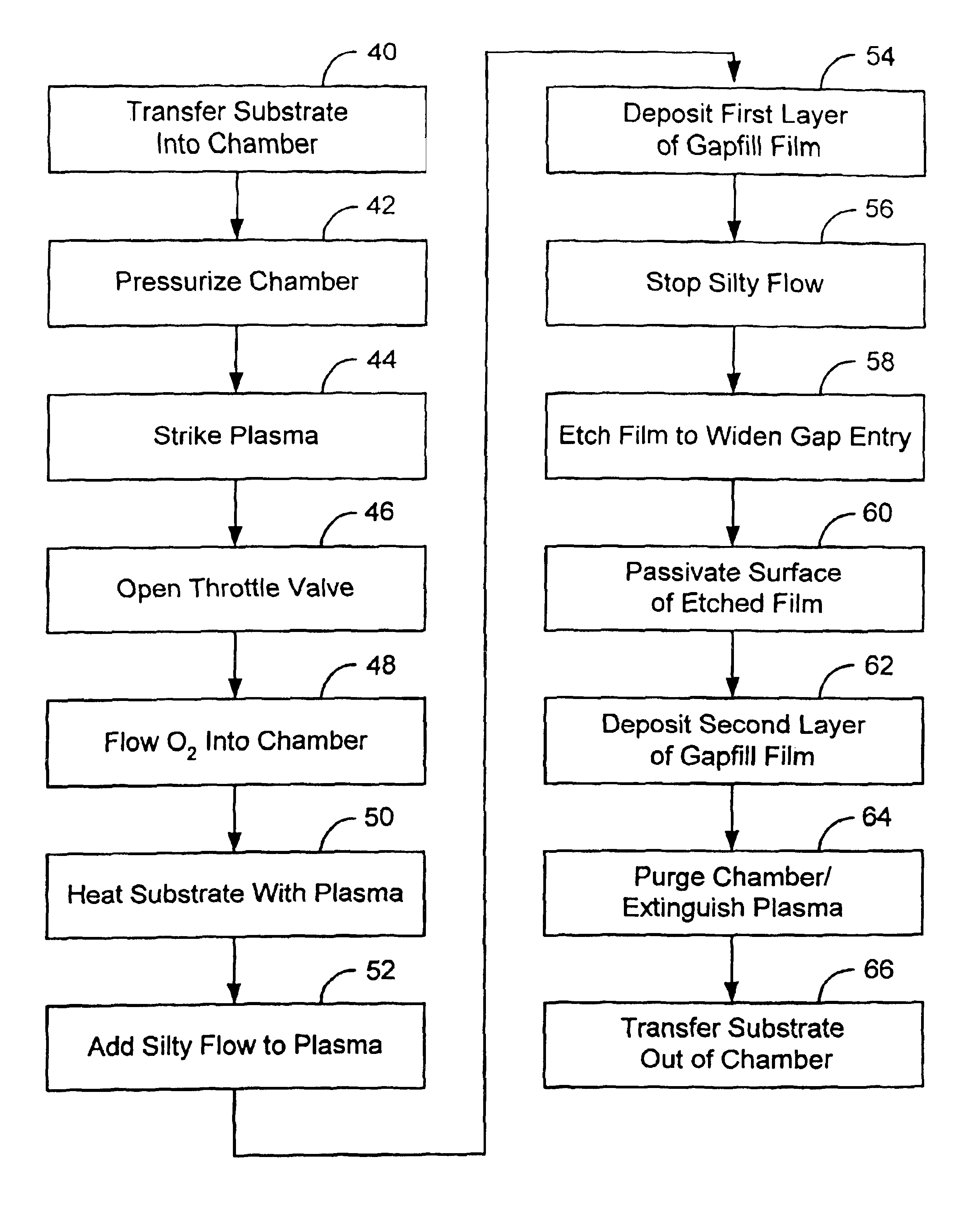
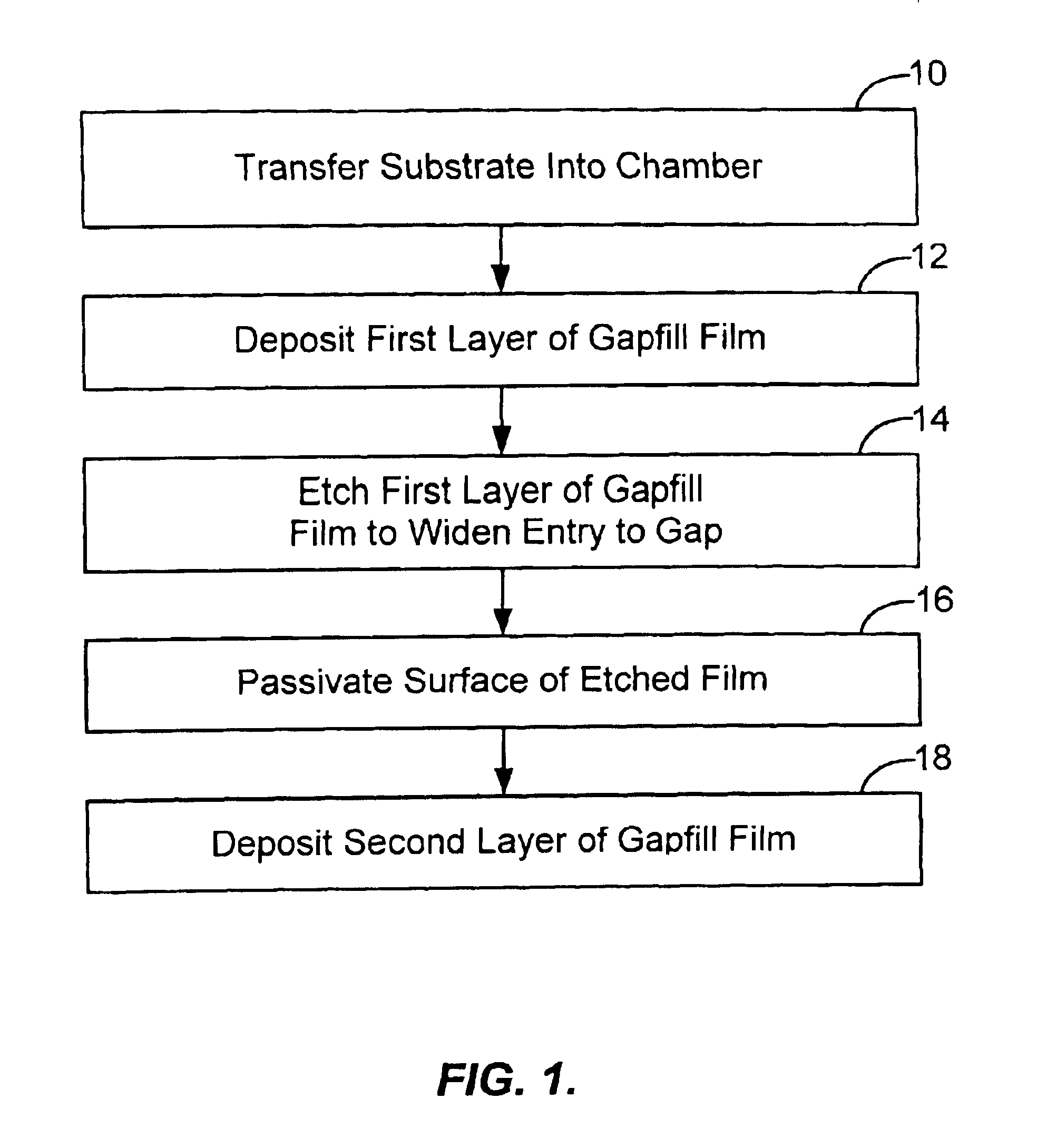
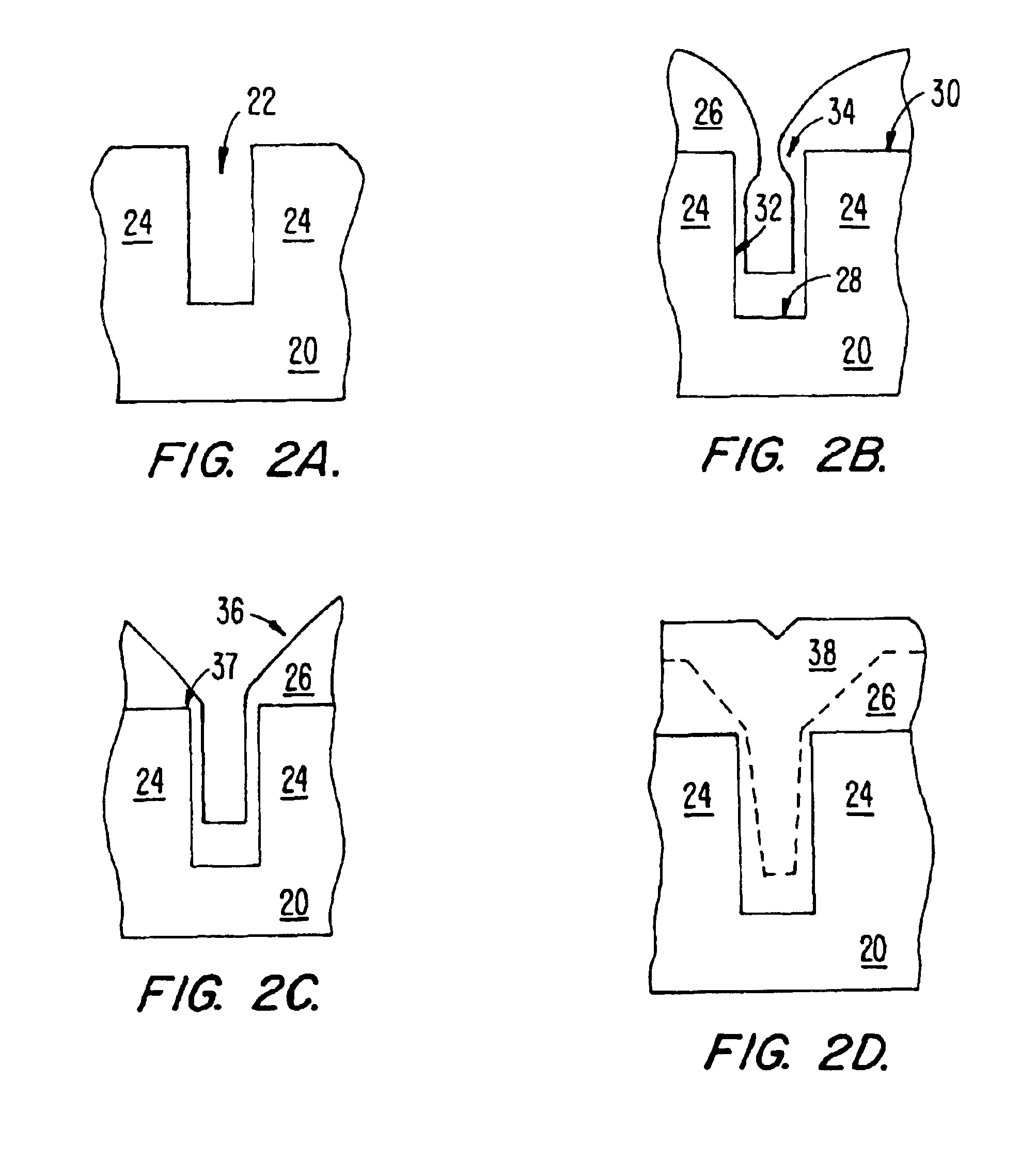
HDP-CVD dep/etch/dep process for improved deposition into high aspect ratio features
PatentInactiveUS6908862B2
Innovation
- An in situ HDP-CVD dep/etch/dep process involving a first film deposition, followed by etching with a halogen etchant, passivation with an oxygen-containing plasma, and subsequent deposition using a second gaseous mixture to achieve 100% gapfill in high aspect ratio features, particularly for semiconductor applications.

Method and apparatus for asymmetric selective physical vapor deposition
PatentWO2019177861A1
Innovation
- The method and apparatus for asymmetric selective physical vapor deposition involve directing streams of material from PVD sources at non-perpendicular angles to the substrate surface, using collimators to control angular ranges, and linearly scanning the substrate to deposit materials only on specific portions of features, such as top and sidewalls, enabling asymmetric deposition profiles while maintaining uniformity across all features.


Environmental Impact of Advanced CVD Processes
The environmental implications of advanced CVD processes for complex geometries present multifaceted challenges that require comprehensive assessment across the entire process lifecycle. Traditional CVD operations already generate significant environmental concerns through precursor consumption, energy utilization, and waste generation, but the pursuit of enhanced selectivity in complex geometries introduces additional environmental considerations that must be carefully evaluated.
Energy consumption represents one of the most significant environmental impacts in selective CVD processes. Advanced temperature control systems, extended processing times, and sophisticated vacuum systems required for achieving high selectivity in complex geometries substantially increase power demands. The need for precise thermal management across intricate three-dimensional structures often necessitates higher operating temperatures and longer processing cycles, directly correlating with increased carbon footprint and operational costs.
Chemical precursor utilization efficiency becomes critically important when considering environmental sustainability. Selective CVD processes for complex geometries typically require specialized precursors with enhanced reactivity profiles, many of which are synthesized through energy-intensive chemical processes. The selectivity enhancement often comes at the cost of reduced precursor utilization efficiency, leading to increased waste generation and higher consumption of raw materials per unit of deposited material.
Waste stream management poses significant challenges in advanced CVD operations. The pursuit of selectivity often involves the use of masking materials, sacrificial layers, and specialized cleaning agents that generate additional waste streams requiring proper treatment and disposal. Unreacted precursors, byproducts from surface reactions, and cleaning solvents contribute to a complex mixture of chemical wastes that demand sophisticated treatment protocols to prevent environmental contamination.
Atmospheric emissions from selective CVD processes require careful monitoring and control. The enhanced chemical reactivity needed for selective deposition often produces volatile organic compounds and potentially hazardous byproducts that must be captured and treated before atmospheric release. Advanced scrubbing systems and emission control technologies become essential components of environmentally responsible CVD operations.
The development of green chemistry approaches in CVD precursor design offers promising pathways for reducing environmental impact. Research into biodegradable precursors, water-based chemistries, and lower-temperature processing conditions demonstrates potential for maintaining selectivity performance while minimizing environmental consequences. These innovations represent critical areas for continued development in sustainable CVD technology advancement.
Process Integration Challenges in Selective CVD Manufacturing
Process integration challenges in selective CVD manufacturing represent one of the most critical bottlenecks in achieving high-quality deposition on complex geometries. The fundamental difficulty lies in maintaining precise control over multiple interdependent process parameters while ensuring uniform selectivity across intricate three-dimensional structures. Traditional CVD systems were primarily designed for planar substrates, making their adaptation to complex geometries inherently problematic.
Temperature uniformity emerges as a primary integration challenge, particularly when dealing with substrates featuring varying thermal masses and surface orientations. Complex geometries create thermal gradients that directly impact precursor decomposition kinetics and surface reaction rates. These variations lead to non-uniform selectivity, where some regions experience desired selective deposition while others suffer from unwanted nucleation or inadequate film growth.
Precursor delivery and mass transport limitations become exponentially more complex in confined spaces and high-aspect-ratio features. The integration of gas delivery systems must account for diffusion limitations, residence time variations, and potential precursor depletion effects. These factors create spatial variations in precursor concentration, directly compromising selectivity uniformity across the substrate.
Surface preparation and cleaning integration present additional complications in manufacturing environments. Complex geometries often require specialized cleaning protocols and surface treatments that must be seamlessly integrated into the overall process flow. The challenge intensifies when considering batch-to-batch consistency and the need for in-situ monitoring capabilities.
Real-time process monitoring and control integration face significant technical hurdles due to the limited accessibility of measurement points on complex substrates. Traditional monitoring techniques become inadequate, necessitating the development of advanced sensing technologies and predictive control algorithms. The integration of these systems into existing manufacturing infrastructure requires substantial modifications to both hardware and software platforms.
Contamination control throughout the integrated process chain represents another critical challenge. Complex geometries create additional surfaces and crevices where contaminants can accumulate, potentially compromising selectivity in subsequent processing steps. The integration of effective contamination mitigation strategies without disrupting the overall process flow requires careful optimization of cleaning cycles, environmental controls, and material handling procedures.
Unlock deeper insights with Patsnap Eureka Quick Research — get a full tech report to explore trends and direct your research. Try now!
Generate Your Research Report Instantly with AI Agent
Supercharge your innovation with Patsnap Eureka AI Agent Platform!