

Evaluating Hybrid Bonding For High-Speed Data Transfers
APR 9, 20269 MIN READ
Generate Your Research Report Instantly with AI Agent
PatSnap Eureka helps you evaluate technical feasibility & market potential.
Hybrid Bonding Technology Background and Objectives
Hybrid bonding technology represents a revolutionary advancement in semiconductor packaging and interconnect solutions, emerging from the convergence of traditional wire bonding and advanced flip-chip technologies. This innovative approach combines the benefits of multiple bonding methodologies to create robust, high-performance connections capable of supporting the ever-increasing demands of modern electronic systems. The technology has evolved from early research in three-dimensional integrated circuits and heterogeneous integration, where conventional single-bonding approaches proved insufficient for complex multi-die configurations.
The fundamental principle of hybrid bonding lies in its ability to simultaneously establish electrical, mechanical, and thermal connections through multiple interface mechanisms. Unlike traditional bonding methods that rely on a single connection type, hybrid bonding integrates copper-to-copper direct bonding, dielectric-to-dielectric adhesion, and micro-bump interconnects within a unified process flow. This multi-modal approach enables unprecedented levels of integration density while maintaining signal integrity across high-frequency operations.
The primary objective of implementing hybrid bonding for high-speed data transfers centers on achieving superior electrical performance through reduced parasitic effects and enhanced signal transmission capabilities. Traditional interconnect solutions face significant limitations when operating at frequencies exceeding several gigahertz, where issues such as crosstalk, signal attenuation, and electromagnetic interference become critical performance bottlenecks. Hybrid bonding addresses these challenges by providing shorter electrical paths, improved impedance control, and enhanced shielding characteristics.
Another key objective involves maximizing bandwidth density while minimizing form factor constraints. Modern applications in artificial intelligence, 5G communications, and high-performance computing demand unprecedented data throughput rates within increasingly compact device architectures. Hybrid bonding enables fine-pitch interconnect arrays with spacing as tight as 10 micrometers, facilitating thousands of parallel data channels within minimal footprint areas.
Thermal management represents an equally critical objective, as high-speed data processing generates substantial heat loads that can degrade performance and reliability. Hybrid bonding's multi-material interface structure provides enhanced thermal conduction pathways, enabling more efficient heat dissipation compared to conventional bonding approaches. This thermal advantage becomes particularly important in applications requiring sustained high-speed operation without performance throttling.
The technology also aims to achieve superior mechanical reliability under various environmental stresses, including thermal cycling, mechanical shock, and long-term aging effects. The distributed stress distribution across multiple bonding interfaces reduces localized failure risks and extends operational lifetime, making hybrid bonding suitable for mission-critical applications requiring exceptional reliability standards.
Market Demand for High-Speed Data Transfer Solutions
The global demand for high-speed data transfer solutions has experienced unprecedented growth driven by the exponential increase in data generation and consumption across multiple industries. Cloud computing infrastructure, artificial intelligence applications, and edge computing deployments require increasingly sophisticated interconnect technologies capable of handling massive data volumes with minimal latency. Traditional copper-based interconnects face fundamental physical limitations in bandwidth and power efficiency, creating substantial market opportunities for advanced bonding technologies.
Data centers represent the largest market segment for high-speed data transfer solutions, with hyperscale operators continuously upgrading their infrastructure to support emerging workloads. The proliferation of machine learning training, real-time analytics, and high-frequency trading applications demands interconnect solutions that can deliver terabits per second of aggregate bandwidth while maintaining strict power consumption targets. Hybrid bonding technology addresses these requirements by enabling direct chip-to-chip connections with superior electrical performance compared to conventional packaging approaches.
The telecommunications sector drives significant demand through the deployment of 5G networks and preparation for 6G infrastructure. Network equipment manufacturers require advanced packaging solutions to achieve the processing speeds necessary for massive MIMO systems, network slicing, and ultra-low latency applications. Hybrid bonding enables the integration of heterogeneous components including digital signal processors, radio frequency circuits, and optical transceivers within compact form factors essential for modern base station designs.
High-performance computing applications in scientific research, financial modeling, and autonomous vehicle development create specialized market segments with stringent performance requirements. These applications often involve complex computational workloads that benefit from tightly coupled processing elements connected through high-bandwidth, low-latency interconnects. Hybrid bonding technology facilitates the creation of advanced multi-chip modules that can deliver the computational density and memory bandwidth required for these demanding applications.
Consumer electronics markets increasingly demand high-speed data transfer capabilities for applications such as augmented reality, virtual reality, and high-resolution display systems. Mobile device manufacturers seek packaging technologies that can support advanced camera systems, neural processing units, and high-speed wireless connectivity while maintaining compact device profiles and acceptable power consumption levels.
The automotive industry represents an emerging market segment as vehicles incorporate more sophisticated electronic systems for autonomous driving, infotainment, and vehicle-to-everything communication. These applications require robust interconnect solutions capable of operating reliably in harsh environmental conditions while delivering the performance necessary for safety-critical functions.
Current State and Challenges of Hybrid Bonding Technology
Hybrid bonding technology has emerged as a critical enabler for high-speed data transfer applications, representing a significant advancement over traditional wire bonding and flip-chip interconnection methods. This technology combines direct copper-to-copper bonding with dielectric-to-dielectric bonding at the wafer or die level, enabling unprecedented interconnect density and electrical performance. Currently, the technology is primarily deployed in advanced memory applications, high-performance computing processors, and emerging artificial intelligence accelerators where bandwidth requirements exceed conventional packaging capabilities.
The global landscape of hybrid bonding technology is dominated by a few key regions, with Taiwan, South Korea, and advanced foundries in the United States leading development efforts. TSMC has achieved commercial production using hybrid bonding for their advanced packaging solutions, while Samsung and SK Hynix have implemented the technology in high-bandwidth memory products. Intel's Foveros technology represents another significant implementation, demonstrating the technology's viability for heterogeneous integration applications.
Despite these successes, several fundamental challenges continue to constrain widespread adoption of hybrid bonding technology. Surface preparation and cleanliness requirements represent the most critical technical hurdle, as even nanometer-scale contamination can prevent proper bonding formation. The technology demands extremely tight surface roughness specifications, typically requiring root mean square roughness values below 0.3 nanometers, which pushes current chemical mechanical planarization processes to their limits.
Thermal management during the bonding process presents another significant challenge, particularly for temperature-sensitive devices. The annealing temperatures required for optimal bond strength, typically ranging from 200°C to 400°C, can adversely affect underlying device performance and reliability. This thermal budget constraint becomes increasingly problematic as device geometries shrink and thermal sensitivity increases.
Alignment accuracy requirements pose substantial manufacturing challenges, with typical specifications demanding sub-micron precision across entire wafer surfaces. Current lithography and bonding equipment struggle to maintain these tolerances consistently, leading to yield limitations that impact commercial viability. The technology also faces scalability challenges related to wafer-level uniformity, as process variations across large wafer areas can result in non-uniform bonding quality.
Cost considerations remain a significant barrier to broader adoption, as hybrid bonding requires specialized equipment, extended process times, and higher material consumption compared to conventional assembly methods. The technology's complexity also demands enhanced process monitoring and quality control systems, further increasing manufacturing overhead and capital requirements for implementation.
Current Hybrid Bonding Solutions for Data Transfer
01 High-speed data transmission through hybrid bonding interfaces
Hybrid bonding technology enables high-speed data transfer by creating direct electrical connections between bonded chips or substrates. This approach minimizes signal path length and reduces parasitic capacitance and inductance, allowing for faster data transmission rates. The direct metal-to-metal and dielectric-to-dielectric bonding provides improved signal integrity and reduced latency compared to traditional interconnection methods.- High-speed data transmission through hybrid bonding interfaces: Hybrid bonding technology enables high-speed data transfer by creating direct electrical connections between chips or substrates through metal-to-metal and dielectric-to-dielectric bonding. This approach minimizes signal path length and reduces parasitic capacitance and inductance, allowing for faster data transmission rates. The technology supports multi-gigabit per second data transfer speeds by optimizing the physical interface between bonded components and reducing signal degradation.
- Signal integrity optimization in hybrid bonded structures: Maintaining signal integrity is crucial for achieving high data transfer speeds in hybrid bonding applications. Techniques include impedance matching, controlled signal routing, and minimizing crosstalk between adjacent interconnects. Advanced design methodologies ensure that signal quality is preserved across the bonded interface, enabling reliable high-speed communication. Proper alignment and bonding quality directly impact the electrical performance and data transfer capabilities.
- Parallel data transmission architectures using hybrid bonding: Hybrid bonding enables the implementation of wide parallel data buses by providing numerous simultaneous electrical connections between bonded components. This parallel architecture significantly increases aggregate data transfer bandwidth compared to traditional serial interfaces. The technology allows for dense interconnect arrays that support multiple data channels operating concurrently, thereby multiplying effective data transfer speeds.
- Thermal management for sustained high-speed data transfer: Effective thermal management is essential for maintaining high data transfer speeds in hybrid bonded systems, as heat generation can limit performance. Design strategies include thermal interface optimization, heat dissipation pathways through the bonded structure, and thermal coupling between components. Proper thermal design ensures that components can operate at maximum data transfer rates without thermal throttling or reliability degradation.
- Advanced packaging configurations for enhanced bandwidth: Hybrid bonding enables novel packaging configurations such as chip-on-chip, chip-on-wafer, and three-dimensional stacking that dramatically increase data transfer bandwidth. These configurations reduce interconnect distances and allow for massive parallel connectivity between processing elements. The technology supports heterogeneous integration where different chip types can be bonded together with optimized high-speed interfaces tailored to specific data transfer requirements.
02 Optimized interconnect density for enhanced bandwidth
Increasing the density of interconnects in hybrid bonding structures significantly improves data transfer bandwidth. Fine-pitch bonding techniques allow for a greater number of signal paths within a given area, enabling parallel data transmission and higher aggregate throughput. The reduced pitch between connections also shortens signal propagation distances, contributing to faster data transfer speeds.Expand Specific Solutions03 Signal integrity enhancement through impedance matching
Proper impedance matching in hybrid bonding structures is critical for maintaining signal integrity at high data transfer speeds. Design techniques that control the electrical characteristics of bonding interfaces help minimize signal reflection and crosstalk. This includes optimizing the geometry and materials of the bonding pads and interconnects to achieve consistent impedance throughout the signal path.Expand Specific Solutions04 Advanced materials for reduced signal loss
The selection of materials with low electrical resistance and dielectric loss is essential for achieving high data transfer speeds in hybrid bonding applications. Advanced conductor materials and low-k dielectrics reduce signal attenuation and power consumption. These materials enable longer transmission distances and higher frequencies while maintaining signal quality and reducing thermal issues.Expand Specific Solutions05 Three-dimensional integration for parallel data pathways
Three-dimensional stacking using hybrid bonding creates multiple parallel data pathways between vertically integrated chips, dramatically increasing overall data transfer capacity. This architecture reduces the distance data must travel and allows for massive parallelism in data transmission. The vertical integration also enables heterogeneous integration of different technologies optimized for specific functions.Expand Specific Solutions
Key Players in Hybrid Bonding and Semiconductor Industry
The hybrid bonding technology for high-speed data transfers represents an emerging market segment within the broader semiconductor packaging and interconnect industry, currently in its early commercialization phase with significant growth potential driven by increasing demands for higher bandwidth and lower latency in data centers and telecommunications infrastructure. The market demonstrates substantial scale opportunities, particularly in 5G networks, cloud computing, and AI applications, with major telecommunications equipment manufacturers like Huawei Technologies, ZTE Corp., Samsung Electronics, and Ericsson leading development efforts alongside specialized companies such as Adeia Semiconductor Bonding Technologies and research institutions like Southeast University and Electronics & Telecommunications Research Institute. Technology maturity varies across implementations, with companies like Qualcomm and NTT advancing practical applications while others focus on foundational research, indicating a competitive landscape where established players leverage existing market positions while emerging specialists drive innovation in bonding methodologies and materials science.
Huawei Technologies Co., Ltd.
Technical Solution: Huawei has developed hybrid bonding solutions integrated into their high-speed communication infrastructure and data center equipment. Their approach combines traditional wire bonding with advanced flip-chip technologies to optimize signal transmission in 5G base stations and optical networking equipment. The company's hybrid bonding implementation focuses on thermal management and signal integrity for applications requiring data rates up to 400Gbps. Their technology incorporates proprietary materials and bonding processes designed to minimize insertion loss and crosstalk in high-density interconnect scenarios. Huawei's solutions are particularly optimized for their telecom equipment where reliable high-speed data transfer is critical for network performance.
Strengths: Strong integration with telecom infrastructure and extensive R&D resources for high-speed applications. Weaknesses: Geopolitical restrictions limiting global market access and technology sharing constraints.
Telefonaktiebolaget LM Ericsson
Technical Solution: Ericsson has developed hybrid bonding solutions for their 5G radio equipment and network infrastructure products, focusing on high-speed backhaul and fronthaul data transmission requirements. Their technology combines advanced packaging techniques with optimized interconnect designs to support data rates exceeding 100Gbps in base station applications. The hybrid bonding implementation incorporates specialized materials and processes designed to maintain signal integrity across wide temperature ranges typical in outdoor telecommunications equipment. Ericsson's solutions emphasize reliability and long-term performance stability, critical for telecommunications infrastructure deployment. Their approach integrates hybrid bonding with advanced thermal management systems to ensure consistent performance in demanding environmental conditions.
Strengths: Strong telecommunications infrastructure expertise and proven reliability in harsh operating environments. Weaknesses: Technology development primarily focused on telecom applications with limited diversification into other high-speed data markets.
Core Patents in Hybrid Bonding for High-Speed Applications
Hybrid bonded interconnect bridging
PatentActiveUS12107075B2
Innovation
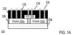
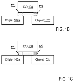
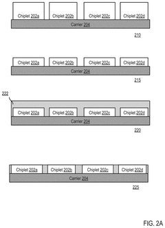
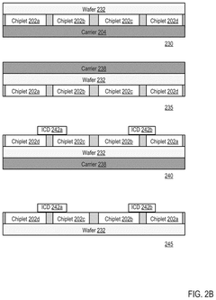
- The use of a hybrid bond, comprising a copper bond and an oxide bond, for direct interconnect die coupling to chiplets, enabling finer pitch connections less than 10 micrometers, along with trans-silicon via connections, conductive pillars, and fluorosilicate glass dielectric layers for improved signal transfer and power distribution.
Hybrid bonding for semiconductor device assemblies
PatentActiveUS12532780B2
Innovation
- The application of a copper nitride composite material on bond pads, formed through a microwave plasma process, acts as an oxidation barrier and facilitates interconnection between bond pads, decomposing during thermal annealing to form gap-free metal-metal bonds.


Thermal Management in High-Speed Hybrid Bonding
Thermal management represents one of the most critical challenges in high-speed hybrid bonding applications, where elevated data transfer rates generate substantial heat that can compromise both performance and reliability. The intimate contact between bonded surfaces in hybrid bonding creates unique thermal pathways that require careful consideration during design and implementation phases.
The fundamental thermal challenge stems from the increased power density associated with high-speed signal transmission through hybrid bonded interfaces. As data rates exceed 100 Gbps, the electrical losses within the bonding materials and interconnect structures generate localized heating that can reach temperatures exceeding 85°C under continuous operation. This thermal buildup directly impacts signal integrity through increased electrical resistance and potential delamination of bonded interfaces.
Heat dissipation in hybrid bonding systems follows complex three-dimensional pathways through the bonded materials, substrate layers, and surrounding packaging structures. The thermal conductivity mismatch between different bonding materials, typically ranging from 1.5 W/mK for polymer-based bonds to 150 W/mK for metallic interconnects, creates thermal bottlenecks that concentrate heat in specific regions. These hotspots can cause thermal expansion mismatches leading to mechanical stress and potential bond failure.
Advanced thermal management strategies for high-speed hybrid bonding incorporate both passive and active cooling approaches. Passive solutions include optimized thermal interface materials with enhanced conductivity, strategic placement of thermal vias, and heat spreading layers integrated within the bonding stack. Active cooling methods involve micro-channel cooling systems and thermoelectric coolers positioned in proximity to high-power bonding regions.
Temperature monitoring and control systems play essential roles in maintaining optimal operating conditions. Real-time thermal sensing through embedded temperature sensors enables dynamic thermal management, allowing systems to adjust operating parameters or activate cooling mechanisms when predetermined temperature thresholds are exceeded. This adaptive approach ensures consistent performance while preventing thermal-induced failures.
The integration of thermal simulation tools during the design phase enables prediction of temperature distributions and identification of potential thermal issues before physical implementation. Computational fluid dynamics modeling combined with finite element thermal analysis provides insights into heat flow patterns and enables optimization of cooling strategies specific to hybrid bonding configurations.
Signal Integrity Optimization in Hybrid Bonded Systems
Signal integrity optimization represents a critical engineering challenge in hybrid bonded systems designed for high-speed data transfers. The intimate physical connection achieved through hybrid bonding creates unique electromagnetic environments that require sophisticated modeling and mitigation strategies to maintain signal quality across the interconnect interface.
The primary signal integrity concerns in hybrid bonded systems stem from impedance discontinuities at the bonding interface. Unlike traditional wire bonding or flip-chip connections, hybrid bonding creates direct metal-to-metal and dielectric-to-dielectric contacts that can introduce subtle but significant impedance variations. These variations manifest as reflections, crosstalk, and signal distortion that become increasingly problematic as data rates exceed 25 Gbps per channel.
Crosstalk mitigation in hybrid bonded architectures requires careful consideration of the three-dimensional field coupling between adjacent signal paths. The reduced separation distances inherent in hybrid bonding can exacerbate near-end and far-end crosstalk, particularly in dense I/O configurations. Advanced ground plane design and strategic via placement become essential for creating effective isolation between high-speed differential pairs.
Power delivery network optimization plays a crucial role in maintaining signal integrity within hybrid bonded systems. The low-impedance connection provided by hybrid bonding enables more efficient power distribution, but also creates new challenges in managing simultaneous switching noise and ground bounce. Decoupling capacitor placement and power plane design must account for the altered current return paths created by the bonded interface.
Electromagnetic modeling of hybrid bonded systems requires sophisticated simulation tools capable of handling the multi-scale nature of these interconnects. Full-wave electromagnetic solvers must accurately capture both the microscopic details of the bonded interface and the macroscopic behavior of the complete system. Time-domain and frequency-domain analysis techniques provide complementary insights into signal propagation characteristics and potential optimization opportunities.
Advanced equalization and signal conditioning techniques become increasingly important as hybrid bonded systems push toward higher data rates. Pre-emphasis, de-emphasis, and adaptive equalization algorithms must be tailored to compensate for the specific channel characteristics introduced by the hybrid bonding process, including any frequency-dependent losses or phase distortions inherent in the bonded interface structure.
Unlock deeper insights with PatSnap Eureka Quick Research — get a full tech report to explore trends and direct your research. Try now!
Generate Your Research Report Instantly with AI Agent
Supercharge your innovation with PatSnap Eureka AI Agent Platform!