

Evaluating the Threshold Voltage Variability in VLSI
MAR 7, 20269 MIN READ
Generate Your Research Report Instantly with AI Agent
PatSnap Eureka helps you evaluate technical feasibility & market potential.
VLSI Threshold Voltage Evolution and Research Objectives
The evolution of Very Large Scale Integration (VLSI) technology has been fundamentally driven by the relentless pursuit of Moore's Law, which predicted the doubling of transistor density every two years. This scaling trajectory has led to dramatic reductions in transistor dimensions, from micrometers in the 1970s to today's advanced nodes at 3nm and below. However, as device dimensions approach atomic scales, threshold voltage variability has emerged as one of the most critical challenges threatening the continued advancement of semiconductor technology.
Threshold voltage represents the minimum gate voltage required to create a conducting channel between source and drain terminals in a MOSFET device. Historically, when transistors were relatively large, statistical variations in threshold voltage were negligible compared to the nominal operating voltage. The manufacturing process variations, dopant fluctuations, and geometric irregularities had minimal impact on overall circuit performance due to the averaging effect across large device areas.
The transition from planar to three-dimensional device architectures, including FinFET and Gate-All-Around (GAA) structures, has introduced new complexities in threshold voltage control. While these advanced architectures offer improved electrostatic control and reduced short-channel effects, they have simultaneously introduced novel sources of variability related to fin width variations, sidewall roughness, and complex stress engineering techniques.
Contemporary VLSI design faces unprecedented challenges as threshold voltage variations now represent a significant percentage of the supply voltage, particularly in low-power applications. Random dopant fluctuations, line edge roughness, metal gate granularity, and high-k dielectric thickness variations contribute to device-to-device threshold voltage mismatches that can severely impact circuit functionality and yield.
The primary research objectives in addressing threshold voltage variability encompass multiple interconnected domains. Process technology development aims to minimize the root causes of variation through advanced lithography techniques, atomic layer deposition for precise thickness control, and innovative doping methodologies. Circuit design objectives focus on developing robust architectures that can tolerate increased variability while maintaining performance targets.
Statistical modeling and characterization represent another crucial research frontier, requiring sophisticated measurement techniques and predictive models that can accurately capture the complex interactions between various sources of variation. The development of machine learning-based approaches for variation prediction and compensation has become increasingly important for next-generation technology nodes.
The ultimate goal extends beyond mere variation reduction to encompass comprehensive design-for-variability methodologies that enable continued scaling while ensuring reliable operation across diverse application domains, from high-performance computing to ultra-low-power Internet of Things devices.
Market Demand for Reliable VLSI with Stable Vth
The semiconductor industry faces unprecedented challenges as device scaling continues toward sub-nanometer nodes, where threshold voltage variability has emerged as a critical reliability concern. Modern VLSI systems require increasingly stringent performance specifications, driving substantial market demand for devices with stable threshold voltage characteristics. This demand spans across multiple application domains, from high-performance computing processors to safety-critical automotive electronics, where voltage fluctuations can compromise system functionality and reliability.
Consumer electronics manufacturers are experiencing growing pressure to deliver products with extended operational lifespans and consistent performance metrics. Mobile device processors, graphics processing units, and system-on-chip solutions must maintain stable threshold voltages across varying environmental conditions and aging cycles. The proliferation of Internet of Things devices has further amplified this requirement, as these systems often operate in harsh environments with limited maintenance opportunities, necessitating robust voltage stability over extended periods.
The automotive sector represents a particularly demanding market segment for stable threshold voltage VLSI components. Advanced driver assistance systems, autonomous vehicle controllers, and electric vehicle power management units require exceptional reliability standards. Threshold voltage drift in these applications can lead to timing violations, power consumption anomalies, and potential safety hazards, creating substantial liability concerns for manufacturers.
Data center and cloud computing infrastructure providers constitute another significant market driver for reliable VLSI with stable threshold voltages. Server processors and memory controllers experiencing voltage variability can result in computational errors, system crashes, and data integrity issues. The economic impact of such failures in large-scale computing environments has intensified the focus on threshold voltage stability as a key procurement criterion.
Emerging applications in artificial intelligence and machine learning accelerators have introduced new reliability requirements. Neural network processors and specialized AI chips must maintain consistent computational accuracy across extended training and inference cycles. Threshold voltage variations can introduce computational drift, affecting model accuracy and requiring frequent recalibration, which impacts operational efficiency and cost-effectiveness.
The market demand extends beyond traditional digital applications to mixed-signal and analog circuits, where threshold voltage stability directly affects signal integrity and measurement precision. Medical devices, precision instrumentation, and communication systems require exceptional voltage stability to maintain regulatory compliance and performance specifications throughout their operational lifetime.
Current Vth Variability Challenges in Advanced VLSI Nodes
Advanced VLSI nodes operating at 7nm, 5nm, and below face unprecedented threshold voltage variability challenges that fundamentally threaten device reliability and circuit performance. As transistor dimensions shrink to atomic scales, the statistical nature of dopant placement becomes increasingly problematic, with individual dopant atoms significantly impacting device characteristics. Random dopant fluctuation emerges as the dominant source of Vth variation, where the discrete placement of dopant atoms within the channel region creates substantial device-to-device variations that cannot be adequately controlled through traditional manufacturing processes.
Process-induced variations represent another critical challenge category, encompassing line edge roughness, gate oxide thickness fluctuations, and metal gate work function variations. Line edge roughness becomes particularly severe at advanced nodes, where even nanometer-scale variations in gate dimensions translate to significant threshold voltage shifts. The introduction of high-k dielectrics and metal gates, while necessary for continued scaling, introduces additional variability sources through interface trap density variations and work function non-uniformities across the wafer.
Temperature-dependent threshold voltage variations pose increasing challenges as power densities escalate in advanced nodes. Local heating effects create spatial temperature gradients across the die, leading to corresponding Vth variations that impact circuit timing and power consumption. The temperature coefficient of threshold voltage becomes more pronounced in ultra-scaled devices, where reduced thermal mass and increased current densities exacerbate thermal effects.
Aging-related threshold voltage drift mechanisms, including bias temperature instability and hot carrier injection, exhibit accelerated degradation rates in advanced nodes. The reduced gate oxide thickness and higher electric fields characteristic of scaled devices amplify these degradation mechanisms, leading to time-dependent Vth shifts that compromise long-term reliability. Negative bias temperature instability particularly affects PMOS devices, while positive bias temperature instability increasingly impacts NMOS devices in advanced process nodes.
Statistical variations in threshold voltage now exceed 50mV in some advanced node implementations, representing a significant fraction of the total supply voltage. This variability directly impacts yield, performance predictability, and power consumption, necessitating sophisticated compensation techniques and design methodologies to maintain acceptable manufacturing yields and circuit functionality across process, voltage, and temperature corners.
Existing Vth Variability Measurement and Control Solutions
01 Threshold voltage compensation circuits and techniques
Various circuit designs and compensation techniques can be implemented to mitigate threshold voltage variations in VLSI devices. These methods involve feedback mechanisms, calibration circuits, and adaptive biasing schemes that dynamically adjust operating parameters to compensate for threshold voltage shifts. Such techniques help maintain consistent circuit performance across process variations and operating conditions.- Threshold voltage compensation circuits and techniques: Various circuit designs and compensation techniques can be implemented to mitigate threshold voltage variations in VLSI devices. These methods include feedback circuits, calibration schemes, and adaptive biasing techniques that dynamically adjust operating parameters to compensate for threshold voltage shifts. Such approaches help maintain consistent circuit performance across process variations and operating conditions.
- Process control and manufacturing techniques for threshold voltage uniformity: Manufacturing process optimization and control methods can be employed to reduce threshold voltage variability during fabrication. These techniques include precise doping control, improved lithography methods, and advanced annealing processes that enhance uniformity across the wafer. Process monitoring and feedback systems enable real-time adjustments to maintain consistent device characteristics.
- Device structure modifications for reduced variability: Specific transistor structures and geometries can be designed to minimize threshold voltage variations. These include multi-gate devices, strain engineering techniques, and optimized channel designs that provide better control over electrostatic characteristics. Such structural modifications help reduce sensitivity to process variations and improve device matching.
- Statistical modeling and simulation methods: Advanced statistical modeling techniques and simulation tools can be utilized to predict and analyze threshold voltage variability in VLSI circuits. These methods incorporate Monte Carlo simulations, corner analysis, and variability-aware design methodologies that enable designers to account for threshold voltage fluctuations during the design phase. Such approaches facilitate robust circuit design that maintains functionality across expected variation ranges.
- Adaptive body biasing and voltage scaling techniques: Dynamic body biasing and adaptive voltage scaling methods can be implemented to counteract threshold voltage variations during operation. These techniques adjust substrate bias voltages or supply voltages based on detected performance metrics or environmental conditions. Such adaptive approaches enable optimization of power consumption and performance while compensating for threshold voltage shifts due to process variations, temperature changes, and aging effects.
02 Process control and manufacturing techniques for threshold voltage uniformity
Manufacturing process optimization methods focus on reducing threshold voltage variability through improved fabrication techniques. These approaches include precise control of doping profiles, gate oxide thickness uniformity, and channel engineering. Advanced lithography and implantation techniques are employed to achieve better device matching and reduced statistical variations across the wafer.Expand Specific Solutions03 Statistical modeling and characterization of threshold voltage variations
Methods for characterizing and modeling threshold voltage variability enable better prediction and analysis of device behavior. These techniques involve statistical analysis of device parameters, Monte Carlo simulations, and corner case modeling. Such approaches help designers understand the impact of process variations and design circuits with adequate margins to ensure reliable operation.Expand Specific Solutions04 Body biasing and substrate control techniques
Adaptive body biasing and substrate voltage control methods provide dynamic adjustment of threshold voltages to compensate for variations. These techniques involve applying controlled voltages to the substrate or body terminals of transistors to modulate their threshold voltages. This approach enables post-manufacturing tuning and real-time compensation for temperature and process variations.Expand Specific Solutions05 Design-for-manufacturability approaches for variability reduction
Design methodologies that incorporate variability-aware techniques help create more robust circuits. These approaches include the use of larger device geometries in critical paths, redundancy schemes, and layout optimization techniques that minimize sensitivity to process variations. Circuit topologies are selected to be inherently less sensitive to threshold voltage mismatches, and design rules are established to ensure adequate margins.Expand Specific Solutions
Leading Semiconductor Companies in Vth Management
The threshold voltage variability evaluation in VLSI represents a mature yet evolving technological domain within the advanced semiconductor industry. The market demonstrates significant scale, driven by increasing demand for precision in nanoscale device characterization across consumer electronics, automotive, and high-performance computing applications. Technology maturity varies considerably among key players, with established semiconductor giants like IBM, Toshiba, Texas Instruments, Qualcomm, and Sony Group leading in advanced characterization methodologies and process optimization. Memory specialists including Micron Technology, Samsung Display, and Yangtze Memory Technologies contribute specialized expertise in threshold voltage control for storage applications. EDA leaders like Synopsys provide critical simulation and modeling tools, while emerging players such as DB HITEK and China Star Optoelectronics represent growing regional capabilities. The competitive landscape reflects a consolidating industry where technological leadership increasingly depends on advanced process control and variability mitigation capabilities.
International Business Machines Corp.
Technical Solution: IBM has developed comprehensive threshold voltage variability evaluation methodologies for advanced VLSI nodes. Their approach combines statistical modeling with machine learning algorithms to predict threshold voltage variations across different process corners and environmental conditions. The company utilizes advanced characterization techniques including temperature coefficient analysis and aging effects assessment to ensure robust circuit design. IBM's methodology incorporates Monte Carlo simulations with over 10,000 iterations to capture statistical variations, enabling accurate prediction of yield and performance metrics. Their evaluation framework supports both planar and FinFET technologies, with particular emphasis on sub-7nm processes where threshold voltage control becomes increasingly critical for circuit reliability and power efficiency.
Strengths: Advanced statistical modeling capabilities, comprehensive process coverage, strong research foundation. Weaknesses: High computational complexity, requires extensive characterization data, limited accessibility for smaller design teams.
Synopsys, Inc.
Technical Solution: Synopsys provides industry-leading EDA tools for threshold voltage variability analysis through their HSPICE and PrimeSim platforms. Their solution integrates Monte Carlo analysis with advanced device models to evaluate threshold voltage variations across process, voltage, and temperature conditions. The platform supports statistical compact models that accurately capture device-to-device variations, including random dopant fluctuations and line edge roughness effects. Synopsys' methodology enables designers to perform comprehensive variability analysis with correlation-aware sampling techniques, reducing simulation time by up to 50% while maintaining accuracy. Their tools support advanced nodes down to 3nm technology, incorporating machine learning-based prediction models for faster convergence and improved statistical coverage of threshold voltage distributions.
Strengths: Industry-standard tools, comprehensive device model support, efficient simulation algorithms. Weaknesses: High licensing costs, steep learning curve, requires significant computational resources for large-scale analysis.
Advanced Techniques for Threshold Voltage Characterization
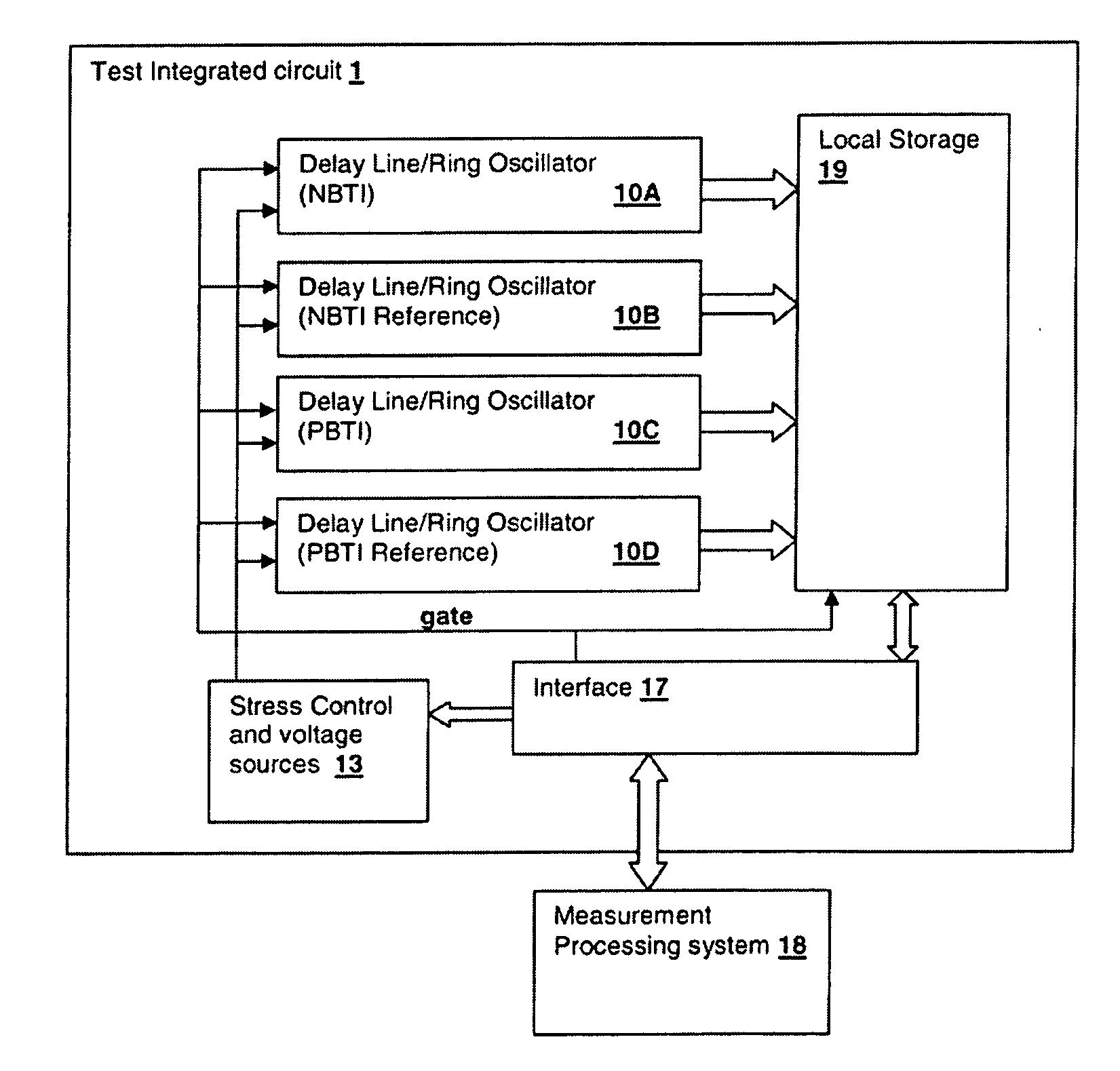
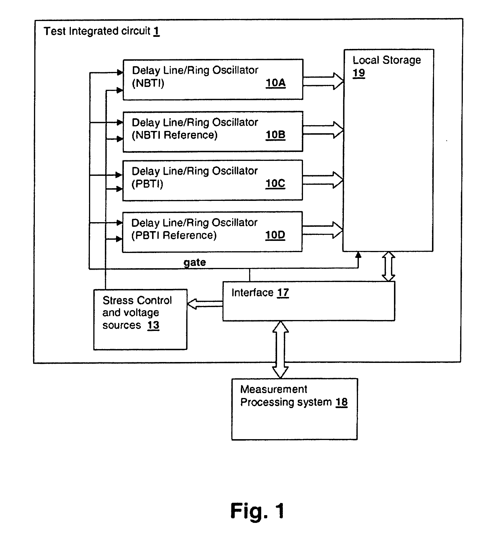
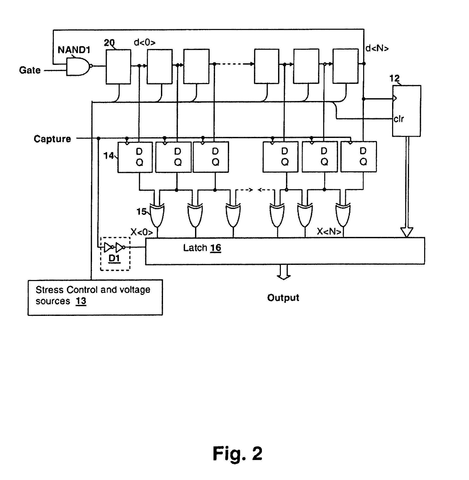
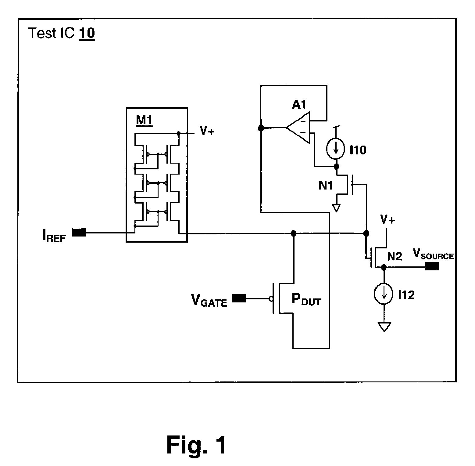
Delay-Based Bias Temperature Instability Recovery Measurements for Characterizing Stress Degradation and Recovery
PatentInactiveUS20090319202A1
Innovation
- A circuit and method using a delay line or ring oscillator with stress-induced NBTI or PBTI effects, where stress is applied and then removed to measure threshold voltage changes, employing edge detection and overflow counters for high-resolution frequency measurements, allowing for sub-microsecond range characterization and repetitive stress simulations.

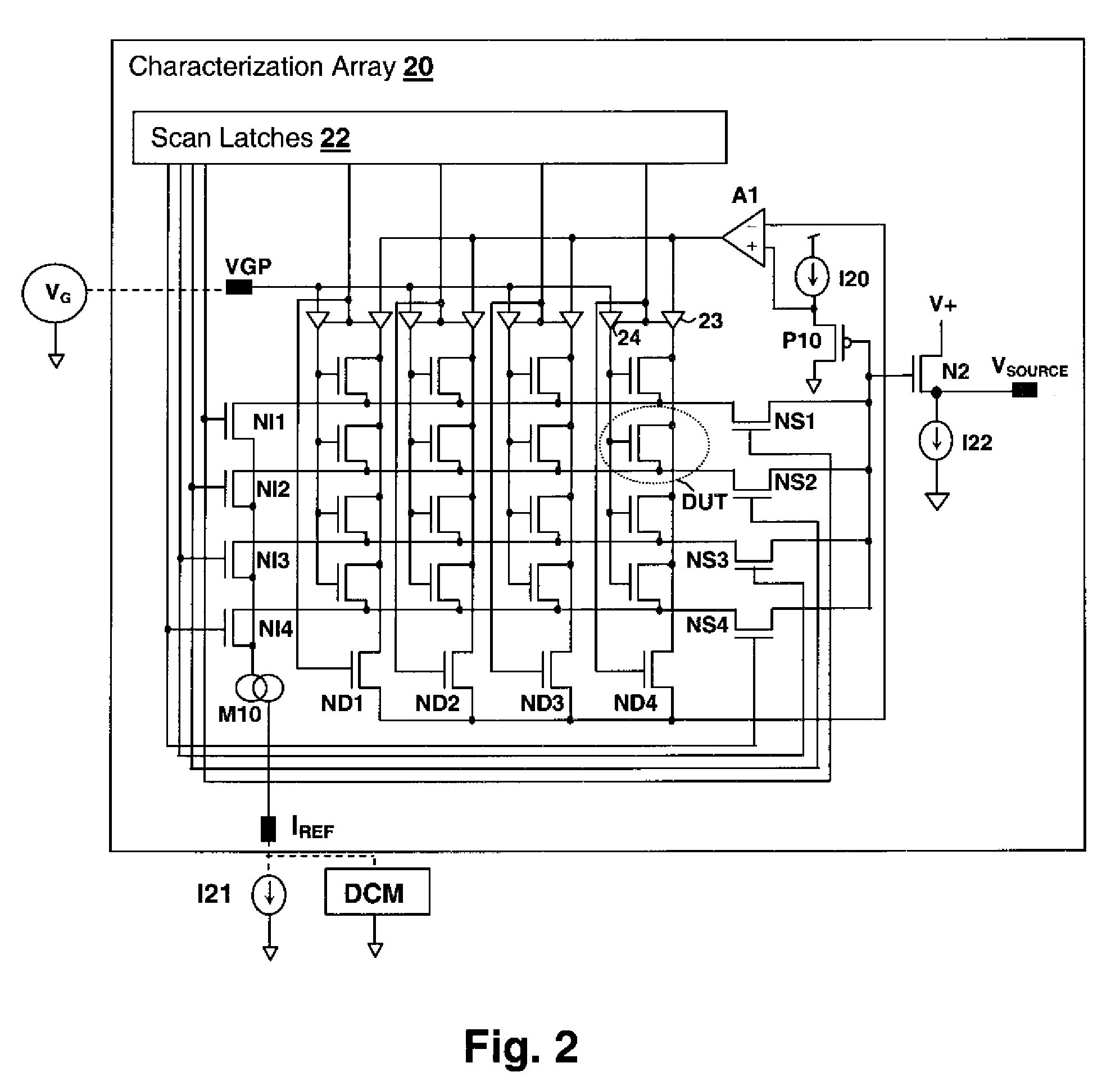
Array-based early threshold voltage recovery characterization measurement
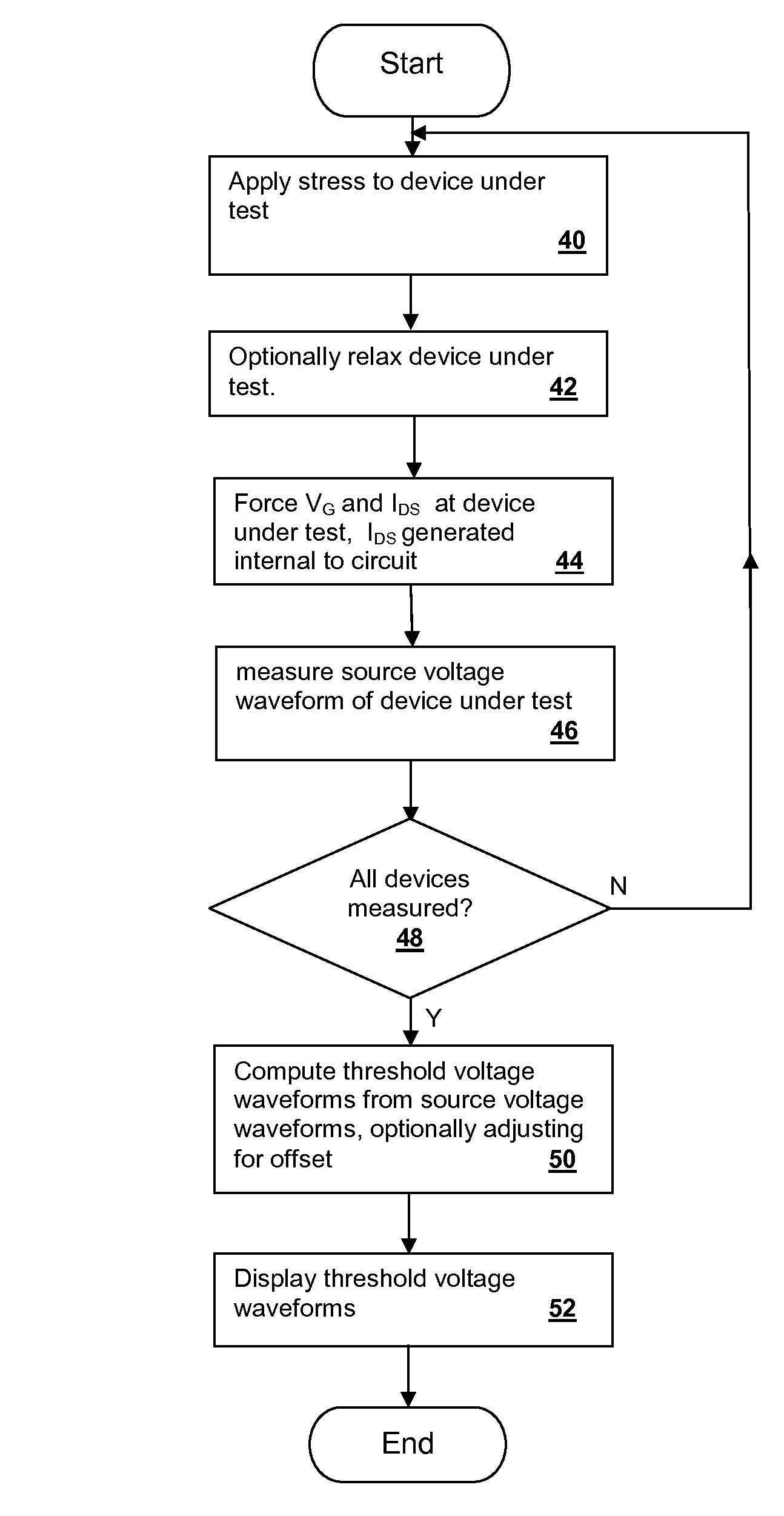
PatentInactiveUS7868640B2
Innovation
- A characterization circuit and methodology that provides a constant drain-source current to the device under test, allowing for the measurement of time-varying source voltage waveforms and threshold voltage changes, enabling early detection of NBTI/PBTI effects under actual operating conditions in a logic circuit environment.

Semiconductor Industry Standards for Vth Testing
The semiconductor industry has established comprehensive standards for threshold voltage (Vth) testing to ensure consistent and reliable evaluation of VLSI devices across different manufacturers and applications. These standards are primarily governed by organizations such as JEDEC Solid State Technology Association, IEEE, and International Electrotechnical Commission (IEC), which provide detailed specifications for measurement methodologies, test conditions, and acceptance criteria.
JEDEC standards, particularly JESD22 series, define the fundamental requirements for Vth characterization in semiconductor devices. These specifications outline precise measurement protocols including drain current levels, gate voltage sweep rates, and temperature conditions during testing. The standards mandate specific current criteria for threshold voltage extraction, typically requiring measurements at drain currents ranging from 1μA to 100μA depending on device geometry and application requirements.
IEEE Standard 1481 provides additional guidelines for statistical analysis of threshold voltage variations, establishing protocols for sample size determination, measurement repeatability, and data reporting formats. This standard emphasizes the importance of multiple measurement points across wafer maps and die locations to capture spatial variations effectively. The specification also defines acceptable measurement uncertainties and calibration requirements for test equipment.
Temperature testing standards require Vth characterization across operational temperature ranges, typically from -40°C to 125°C for commercial applications and extended ranges for automotive and aerospace applications. These standards specify thermal equilibrium requirements, measurement timing, and temperature coefficient calculations to ensure accurate characterization of temperature-dependent variations.
Process control standards integrate Vth testing into manufacturing quality systems, defining control limits, statistical process control methodologies, and corrective action protocols. These standards establish correlation requirements between different test equipment and measurement sites, ensuring consistency across global manufacturing facilities.
Recent updates to industry standards have incorporated advanced statistical methods for variability analysis, including Monte Carlo simulation requirements and machine learning-based prediction models. These evolving standards reflect the increasing complexity of modern VLSI devices and the need for more sophisticated characterization techniques to maintain manufacturing yield and device reliability in advanced technology nodes.
Process Variation Impact on VLSI Yield and Reliability
Process variations in VLSI manufacturing represent one of the most critical challenges affecting semiconductor yield and long-term reliability. These variations stem from inherent limitations in fabrication processes, where parameters such as gate length, oxide thickness, dopant concentration, and metal line width cannot be controlled with absolute precision across entire wafers and between different manufacturing lots.
The impact on yield manifests primarily through parametric failures, where devices fail to meet specified performance criteria despite being functionally correct. Threshold voltage variations directly contribute to timing failures, as transistors with higher threshold voltages switch slower, potentially causing setup time violations in critical paths. Conversely, devices with lower threshold voltages may exhibit excessive leakage current, leading to power consumption failures or reduced noise margins.
Statistical analysis reveals that process variations follow complex distributions that compound across multiple process steps. Random variations, including random dopant fluctuations and line edge roughness, create device-to-device mismatches within the same die. Systematic variations, such as across-wafer gradients and proximity effects, introduce spatial correlations that can cause entire regions of a chip to exhibit similar deviations from nominal behavior.
Reliability implications extend beyond initial manufacturing yield, as process variations influence long-term degradation mechanisms. Devices operating near specification limits due to process variations are more susceptible to aging effects such as bias temperature instability and hot carrier injection. The interaction between initial process-induced parameter shifts and time-dependent degradation creates a compounding reliability risk that must be carefully managed through design margins and screening procedures.
Modern yield enhancement strategies employ sophisticated statistical models to predict and compensate for process variation effects. Design-for-manufacturability techniques, including statistical timing analysis and process-aware design optimization, help maintain acceptable yield levels while minimizing the performance penalties associated with conservative design margins. Advanced process control and adaptive manufacturing techniques continue to evolve as essential tools for managing the growing impact of process variations in scaled VLSI technologies.
Unlock deeper insights with PatSnap Eureka Quick Research — get a full tech report to explore trends and direct your research. Try now!
Generate Your Research Report Instantly with AI Agent
Supercharge your innovation with PatSnap Eureka AI Agent Platform!