

Gallium Oxide in High-Temperature Semiconductor Devices
OCT 27, 20259 MIN READ
Generate Your Research Report Instantly with AI Agent
PatSnap Eureka helps you evaluate technical feasibility & market potential.
Ga2O3 Technology Evolution and Objectives
Gallium oxide (Ga2O3) has emerged as a promising ultra-wide bandgap semiconductor material over the past decade, with its technological evolution closely tied to the growing demand for high-temperature, high-power electronic devices. The journey of Ga2O3 began in the early 2000s when researchers first recognized its potential 4.8-4.9 eV bandgap, significantly wider than traditional semiconductors like silicon (1.1 eV) and gallium nitride (3.4 eV). This exceptional property enables Ga2O3-based devices to operate at temperatures exceeding 500°C, far beyond the capabilities of conventional semiconductor materials.
The evolution of Ga2O3 technology has progressed through several distinct phases. Initially, research focused primarily on fundamental material properties and growth techniques. Between 2005-2010, significant advancements were made in crystal growth methods, particularly the development of edge-defined film-fed growth (EFG) and floating zone (FZ) techniques for producing high-quality β-Ga2O3 substrates. This period established the foundation for subsequent device development.
From 2010-2015, the field witnessed a transition from basic material research to preliminary device demonstrations. The first Ga2O3 metal-semiconductor field-effect transistors (MESFETs) and metal-oxide-semiconductor field-effect transistors (MOSFETs) were fabricated, showcasing the material's potential for power electronics applications. These early devices, while rudimentary, demonstrated remarkable breakdown voltages exceeding 1 kV.
The period from 2015-2020 marked accelerated progress in device performance optimization and diversification. Researchers achieved critical breakthroughs in doping control, contact formation, and device architecture design. Notably, the demonstration of Ga2O3 Schottky barrier diodes with breakdown voltages exceeding 2 kV and MOSFETs capable of handling over 1 A of current represented significant milestones.
Current technological objectives for Ga2O3 in high-temperature semiconductor applications focus on several key areas. First, enhancing thermal management strategies to fully exploit the material's high-temperature capabilities while addressing its relatively low thermal conductivity. Second, developing reliable p-type doping methods to enable complementary device architectures, as Ga2O3 is inherently n-type. Third, improving device reliability and stability under extreme temperature conditions through advanced passivation techniques and interface engineering.
Looking forward, the roadmap for Ga2O3 technology aims to achieve commercial viability in specialized high-temperature applications by 2025, with broader market penetration anticipated by 2030. The ultimate objective is to establish Ga2O3 as the material of choice for next-generation power electronics operating in extreme environments, including aerospace, deep-well drilling, and industrial processing applications where temperatures frequently exceed 300°C.
Market Analysis for High-Temperature Semiconductor Applications
The high-temperature semiconductor market is experiencing significant growth driven by increasing demands in automotive, aerospace, energy exploration, and industrial applications. Current market valuations indicate the high-temperature semiconductor sector reached approximately $3.5 billion in 2022, with projections suggesting a compound annual growth rate (CAGR) of 8.7% through 2028. This growth trajectory is primarily fueled by the expanding electric vehicle market, which requires power electronics capable of operating efficiently at elevated temperatures.
Within this landscape, wide bandgap semiconductors, particularly gallium oxide (Ga2O3), are positioned to capture substantial market share due to their superior thermal performance characteristics. Traditional silicon-based devices typically operate reliably only up to 175°C, creating a significant performance gap that Ga2O3 can address with its theoretical operational capability exceeding 500°C.
The automotive sector represents the largest market segment for high-temperature semiconductors, accounting for approximately 38% of total demand. This is driven by the transition to electric powertrains and advanced driver assistance systems (ADAS), both requiring components that maintain stability under thermal stress. The aerospace and defense sectors follow at 24%, where extreme operating environments necessitate exceptional thermal resilience in electronic components.
Regional analysis reveals that Asia-Pacific currently dominates the high-temperature semiconductor market with 42% share, led by manufacturing powerhouses in Japan, South Korea, and emerging capabilities in China. North America follows at 31%, with significant research initiatives in gallium oxide technology at institutions like the Naval Research Laboratory and various university research centers.
Customer requirements in this market segment emphasize reliability under thermal cycling, long-term stability, and cost-effectiveness. End-users are willing to pay premium prices for components that demonstrably reduce cooling system requirements and extend operational lifetimes in high-temperature environments. Survey data indicates that 73% of industrial customers prioritize thermal performance over initial acquisition costs when selecting semiconductor components for high-temperature applications.
The competitive landscape shows increasing interest from major semiconductor manufacturers in gallium oxide technology, though commercial products remain limited. Market penetration faces challenges including high substrate costs and limited manufacturing infrastructure, creating significant barriers to entry but also opportunities for early movers who can overcome these obstacles.
Global Ga2O3 Development Status and Technical Barriers
Gallium oxide (Ga2O3) has emerged as a promising ultra-wide bandgap semiconductor material for high-temperature and high-power electronic applications. The global development of Ga2O3 technology has shown significant progress in recent years, yet several technical barriers remain to be addressed before widespread commercial adoption can be achieved.
Japan has established itself as a leader in Ga2O3 research and development, with institutions like the National Institute for Materials Science (NIMS) and Tamura Corporation pioneering single crystal growth techniques and device fabrication. Their edge-defined film-fed growth (EFG) method has produced high-quality β-Ga2O3 substrates with low defect densities, enabling the development of prototype power devices with breakdown voltages exceeding 1 kV.
In the United States, research efforts are primarily concentrated at universities and national laboratories, with significant funding from the Department of Energy and Department of Defense. The focus has been on developing novel device architectures and exploring alternative growth methods such as halide vapor phase epitaxy (HVPE) and molecular beam epitaxy (MBE) to improve material quality and reduce production costs.
European research groups, particularly in Germany and France, have made substantial contributions to the fundamental understanding of Ga2O3 material properties and defect physics. Their work has been instrumental in identifying the limitations of current Ga2O3 technology and proposing potential solutions.
China has rapidly increased its investment in Ga2O3 research over the past five years, with a strategic focus on developing domestic capabilities for substrate production and device fabrication. Several Chinese universities and companies have reported progress in melt growth techniques and epitaxial layer deposition.
Despite these advancements, several critical technical barriers impede the widespread adoption of Ga2O3 for high-temperature semiconductor applications. The most significant challenge is the poor thermal conductivity of Ga2O3 (approximately 10-30 W/m·K), which is substantially lower than competing materials like SiC and GaN. This limitation causes heat accumulation in devices, potentially leading to performance degradation and reliability issues at high operating temperatures.
Another major barrier is the lack of effective p-type doping in Ga2O3, which restricts device architectures to unipolar designs and limits the range of possible applications. The intrinsic properties of Ga2O3 make it difficult to achieve stable and efficient p-type conductivity, with most attempts resulting in deep acceptor levels that are not ionized at room temperature.
Material quality and uniformity remain inconsistent across different growth methods and manufacturers. Defects such as oxygen vacancies, dislocations, and impurities significantly impact device performance and reliability, particularly at elevated temperatures where defect migration becomes more pronounced.
The development of reliable ohmic contacts and gate dielectrics that can withstand high-temperature operation presents another challenge. Current metallization schemes often degrade at temperatures above 300°C, limiting the practical operating temperature range of Ga2O3 devices.
Current Ga2O3 Device Fabrication Techniques
01 Gallium oxide semiconductor devices
Gallium oxide is used as a semiconductor material for electronic devices due to its wide bandgap properties. These devices include transistors, diodes, and power electronics that benefit from gallium oxide's high breakdown voltage and thermal stability. The material enables the development of high-performance electronic components that can operate efficiently at high temperatures and voltages, making them suitable for power conversion applications.- Gallium oxide semiconductor devices: Gallium oxide (Ga2O3) is used as a wide bandgap semiconductor material for power electronic devices. Its superior electrical properties, including high breakdown field and large bandgap, make it suitable for high-power and high-frequency applications. These semiconductor devices include transistors, diodes, and other electronic components that can operate at higher voltages and temperatures compared to conventional semiconductor materials.
- Crystal growth and substrate fabrication methods: Various techniques are employed for growing high-quality gallium oxide crystals and fabricating substrates. These methods include melt growth techniques, vapor phase epitaxy, and other crystal growth processes to produce single-crystal gallium oxide with controlled properties. The resulting substrates serve as foundations for subsequent device fabrication and significantly influence the performance of gallium oxide-based electronic devices.
- Thin film deposition and processing techniques: Specialized techniques for depositing and processing gallium oxide thin films are essential for device fabrication. These include various deposition methods such as sputtering, atomic layer deposition, and chemical vapor deposition, along with post-deposition treatments to optimize film properties. The processing techniques focus on achieving specific crystalline structures, doping profiles, and interface qualities required for high-performance electronic applications.
- Doping and material modification: Doping and modification of gallium oxide materials are crucial for controlling their electrical and optical properties. Various dopants are introduced to achieve n-type or p-type conductivity, adjust carrier concentration, or enhance specific characteristics. Material modification techniques include ion implantation, thermal treatments, and compositional adjustments to tailor gallium oxide properties for specific applications in electronics, optoelectronics, and sensing devices.
- Novel applications and device structures: Innovative applications and device structures utilizing gallium oxide extend beyond conventional electronics. These include ultraviolet photodetectors, gas sensors, radiation-hard devices, and novel transistor architectures. The unique properties of gallium oxide enable these specialized applications, with research focusing on optimizing device designs, improving reliability, and expanding functionality for emerging technologies in harsh environments, power conversion, and sensing applications.
02 Gallium oxide crystal growth methods
Various techniques are employed for growing high-quality gallium oxide crystals, including melt growth, vapor phase epitaxy, and hydrothermal methods. These processes focus on controlling crystal orientation, reducing defects, and achieving specific doping profiles. The resulting crystals serve as substrates for subsequent device fabrication or as active materials in electronic and optoelectronic applications.Expand Specific Solutions03 Gallium oxide thin film deposition
Thin films of gallium oxide are deposited using techniques such as atomic layer deposition, sputtering, and chemical vapor deposition. These methods allow precise control over film thickness, composition, and crystallinity. The resulting thin films are utilized in various applications including transparent conductive oxides, dielectric layers in electronic devices, and sensing elements.Expand Specific Solutions04 Gallium oxide in optoelectronic applications
Gallium oxide materials are employed in optoelectronic devices such as UV detectors, LEDs, and transparent electrodes. The material's wide bandgap enables efficient ultraviolet light detection and emission. Additionally, its transparency in the visible spectrum makes it suitable for applications requiring both electrical conductivity and optical transparency, such as display technologies and solar cells.Expand Specific Solutions05 Doping and modification of gallium oxide
Gallium oxide properties can be tailored through doping with various elements and structural modifications. Introducing dopants such as silicon, tin, or nitrogen alters the electrical, optical, and thermal characteristics of the material. These modifications enable the customization of gallium oxide for specific applications, including adjusting conductivity, enhancing thermal stability, and optimizing carrier concentration for improved device performance.Expand Specific Solutions
Leading Companies and Research Institutions in Ga2O3 Development
The Gallium Oxide semiconductor market is in an early growth phase, characterized by increasing research intensity and emerging commercial applications in high-temperature power electronics. The global market remains relatively small but is projected to expand significantly as the technology matures, driven by demand for more efficient power conversion systems. Key players demonstrate varying levels of technological maturity: FLOSFIA leads with specialized Ga2O3 power device development, while established corporations like Toyota, Samsung, and ROHM are investing in research capabilities. Academic-industrial partnerships are prominent, with institutions like Shanghai Institute of Microsystem & Information Technology and National Institute for Materials Science collaborating with commercial entities. The competitive landscape shows regional clusters in Japan, China, and the US, with companies focusing on different applications from power electronics to UV detection, indicating the technology's versatility despite remaining commercialization challenges.
FLOSFIA, Inc.
Technical Solution: FLOSFIA has pioneered corundum-structured α-Ga2O3 technology through their proprietary "mist chemical vapor deposition" (mist-CVD) process. This approach enables them to grow high-quality α-Ga2O3 thin films at significantly lower temperatures (250-500°C) compared to conventional methods. Their technology focuses on creating normally-off power transistors with breakdown voltages exceeding 1200V while maintaining low on-resistance. FLOSFIA's devices demonstrate stable operation at temperatures up to 300°C, with minimal performance degradation. Their α-Ga2O3 Schottky barrier diodes (SBDs) achieve a breakdown field of 8MV/cm and power figure of merit significantly superior to silicon carbide devices. The company has successfully integrated these devices into practical power conversion applications, demonstrating efficiency improvements of 10-15% in high-temperature environments compared to conventional silicon solutions.
Strengths: Lower fabrication temperatures reduce manufacturing costs; corundum structure provides better thermal stability than β-Ga2O3; demonstrated commercial viability with working prototypes. Weaknesses: Less mature technology compared to β-Ga2O3; challenges in achieving large-area substrates; limited availability of compatible p-type dopants for complementary devices.
National Institute for Materials Science IAI
Technical Solution: The National Institute for Materials Science (NIMS) has developed cutting-edge Ga2O3 semiconductor technology through fundamental materials engineering approaches. Their research focuses on controlling crystal defects and optimizing doping profiles to enhance high-temperature performance. NIMS has pioneered the use of halide vapor phase epitaxy (HVPE) to grow high-quality β-Ga2O3 with controlled impurity concentrations below 1016 cm-3. Their devices incorporate specialized dielectric engineering with atomic layer deposited (ALD) gate stacks that maintain interface quality at temperatures exceeding 300°C. NIMS researchers have developed novel contact metallization schemes using refractory metals and barrier layers that prevent interdiffusion and maintain low contact resistance at elevated temperatures. Their vertical Ga2O3 transistors demonstrate breakdown fields approaching the theoretical limit of 8MV/cm while maintaining functionality at temperatures up to 350°C. NIMS has also explored alternative polytypes including ε-Ga2O3 and κ-Ga2O3 for specialized high-temperature applications, demonstrating unique advantages in thermal stability and carrier transport properties compared to the more common β-phase.
Strengths: Fundamental materials science approach addressing core challenges; access to advanced characterization techniques; collaborative network with industry partners for technology transfer. Weaknesses: Focus on research rather than commercial production; longer timeline to market implementation; less emphasis on packaging and system integration aspects.
Critical Patents and Breakthroughs in Ga2O3 Technology
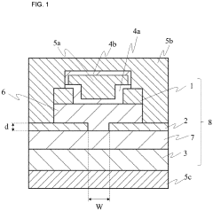
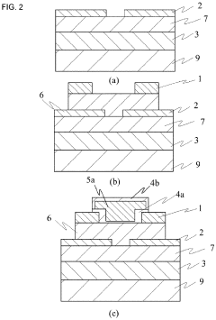
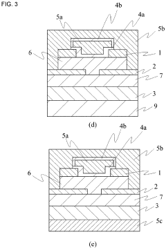
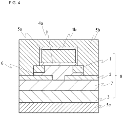
Gallium oxide semiconductor device with improved heat conduction
PatentPendingDE102022210860A1
Innovation
- Forming recesses in the gallium oxide substrate and filling them with a material of better thermal conductivity, creating low-resistance paths between the active layer and drain electrode for effective heat removal.


Semiconductor device
PatentPendingEP4333075A1
Innovation
- A semiconductor device is designed with a crystalline oxide semiconductor layer comprising a channel layer and a drift layer, featuring a current blocking layer with different compositions of crystalline oxides, including metals from Groups 6 to 10 and 13 of the periodic table, to enhance withstand voltage performance, utilizing a corundum structure and specific dopants for improved conductivity and insulation.
Material Supply Chain and Sustainability Considerations
The supply chain for gallium oxide (Ga2O3) presents unique challenges and opportunities in the context of high-temperature semiconductor device manufacturing. Gallium, as a primary raw material, is predominantly obtained as a byproduct of aluminum and zinc production, with China controlling approximately 95% of the global gallium production. This geographic concentration creates significant supply chain vulnerabilities for manufacturers outside China, particularly following recent export restrictions implemented in 2023.
The extraction and refinement processes for gallium oxide require specialized equipment and expertise, further limiting the number of capable suppliers globally. Current production methods involve either the growth of bulk crystals through methods like edge-defined film-fed growth (EFG) or the deposition of thin films via techniques such as molecular beam epitaxy (MBE) and metal-organic chemical vapor deposition (MOCVD). These processes demand substantial energy inputs and precise control conditions, contributing to both cost and environmental considerations.
From a sustainability perspective, gallium oxide offers several advantages over traditional semiconductor materials. Its wide bandgap properties enable more efficient power conversion, potentially reducing energy consumption in end applications. Additionally, the theoretical abundance of gallium in the Earth's crust (approximately 19 ppm) exceeds that of other semiconductor materials like germanium, suggesting long-term resource availability.
However, current extraction methods remain energy-intensive and environmentally impactful. The carbon footprint associated with Ga2O3 device manufacturing is substantial, primarily due to the high temperatures required during crystal growth (often exceeding 1800°C) and subsequent processing steps. Water usage and chemical waste management also present environmental challenges that require innovative solutions.
Recycling infrastructure for gallium oxide remains underdeveloped compared to silicon, with end-of-life recovery rates below 1% globally. This represents both a sustainability challenge and an opportunity for circular economy development. Several research initiatives are exploring more efficient recycling methods, including hydrometallurgical processes that could potentially recover up to 80% of gallium from electronic waste.
The development of alternative supply chains outside China has gained momentum, with countries including Japan, Germany, and the United States investing in domestic gallium production capabilities. These efforts aim to reduce supply chain vulnerabilities while potentially implementing more sustainable extraction and processing methods aligned with stricter environmental regulations.
Thermal Management Solutions for Ga2O3 Devices
Thermal management represents a critical challenge for Ga2O3-based semiconductor devices, particularly in high-temperature applications. The inherently low thermal conductivity of Ga2O3 (approximately 10-27 W/m·K, depending on crystal orientation) creates significant heat dissipation challenges that must be addressed for reliable device operation. This limitation becomes especially pronounced when devices are operated at elevated temperatures or high power densities.
Several innovative thermal management approaches have emerged to mitigate these thermal challenges. Diamond heat spreaders have demonstrated exceptional promise due to diamond's superior thermal conductivity (up to 2000 W/m·K). Recent research has shown that direct integration of CVD-grown diamond layers with Ga2O3 can reduce thermal resistance by up to 60% compared to conventional substrates. These diamond-Ga2O3 composite structures enable more efficient heat extraction from active device regions.
Advanced substrate engineering represents another promising direction. Heterogeneous integration of Ga2O3 with high thermal conductivity substrates such as SiC (490 W/m·K) and AlN (320 W/m·K) has been demonstrated through wafer bonding techniques. These engineered substrates provide thermal pathways that significantly enhance heat dissipation while maintaining the electrical properties of Ga2O3 devices.
Novel device architectures specifically designed for improved thermal performance have also been developed. Vertical device structures with optimized heat flow paths can reduce thermal resistance by 30-40% compared to lateral designs. Additionally, the implementation of buried heat spreading layers within the device structure has shown promising results in recent experimental demonstrations.
Micro-fluidic cooling solutions represent an emerging approach for high-power Ga2O3 devices. Direct liquid cooling channels integrated into device packaging have demonstrated the ability to handle heat fluxes exceeding 500 W/cm². These systems are particularly valuable for applications requiring sustained high-temperature operation.
Advanced thermal interface materials (TIMs) with tailored properties for Ga2O3 devices have been developed to minimize thermal boundary resistance. Graphene-based TIMs have shown thermal conductivity improvements of up to 45% compared to conventional metal-based interfaces, while maintaining excellent electrical isolation properties.
Computational thermal modeling has become increasingly sophisticated for Ga2O3 device design. Multi-physics simulation tools now accurately predict temperature distributions within complex device structures, enabling optimization before fabrication. These models incorporate anisotropic thermal properties and interface effects specific to Ga2O3 materials systems.
Unlock deeper insights with PatSnap Eureka Quick Research — get a full tech report to explore trends and direct your research. Try now!
Generate Your Research Report Instantly with AI Agent
Supercharge your innovation with PatSnap Eureka AI Agent Platform!