

Gallium Oxide in Semiconductor-Based Telecommunications
OCT 27, 20259 MIN READ
Generate Your Research Report Instantly with AI Agent
PatSnap Eureka helps you evaluate technical feasibility & market potential.
Gallium Oxide Semiconductor Evolution and Objectives
Gallium oxide (Ga2O3) has emerged as a promising ultra-wide bandgap semiconductor material, representing a significant evolution in semiconductor technology over the past decade. With a bandgap of approximately 4.8-4.9 eV, it surpasses traditional semiconductors like silicon (1.1 eV) and gallium nitride (3.4 eV), positioning it as a revolutionary material for high-power and high-frequency telecommunications applications.
The historical development of gallium oxide as a semiconductor material can be traced back to the early 2000s, when researchers began exploring its potential electronic properties. However, significant breakthroughs in crystal growth techniques and device fabrication only materialized in the 2010s, marking the beginning of serious consideration for commercial applications. The evolution accelerated when Japanese researchers demonstrated the first gallium oxide transistors with promising performance characteristics around 2012.
From a materials perspective, gallium oxide exists in multiple polymorphs (α, β, γ, δ, and ε), with the β-phase being the most stable and consequently the most extensively studied for semiconductor applications. This phase stability represents a critical advantage in the evolution of gallium oxide technology, as it facilitates more straightforward manufacturing processes compared to other wide bandgap materials.
The technological trajectory of gallium oxide semiconductors has been driven by increasing demands in telecommunications for higher frequency operation, greater power handling capabilities, and improved thermal management. These requirements have become particularly acute with the global deployment of 5G networks and the anticipated needs of future 6G systems, where higher frequencies and data rates necessitate semiconductors capable of operating efficiently under extreme conditions.
Current objectives in gallium oxide semiconductor development focus on several key areas: improving material quality through advanced growth techniques such as halide vapor phase epitaxy (HVPE) and molecular beam epitaxy (MBE); enhancing doping control to achieve desired electrical properties; developing reliable device fabrication processes; and addressing thermal management challenges inherent to the material's relatively low thermal conductivity.
Long-term objectives include the integration of gallium oxide devices into telecommunications infrastructure, particularly in base stations and satellite communications systems where high-power, high-frequency operation is critical. Researchers aim to leverage gallium oxide's theoretical breakdown field of 8 MV/cm—significantly higher than silicon carbide and gallium nitride—to create more efficient power amplifiers and switching devices for next-generation communication systems.
The evolution path also encompasses developing heterogeneous integration techniques to combine gallium oxide with other semiconductor materials, creating hybrid systems that maximize the advantages of each material while mitigating their respective limitations.
Telecommunications Market Demand for Wide Bandgap Materials
The telecommunications industry is experiencing a significant shift towards higher frequency bands and increased power requirements, creating substantial demand for wide bandgap (WBG) semiconductor materials. Traditional silicon-based semiconductors are approaching their physical limitations in terms of power handling, frequency response, and thermal management, particularly in 5G and upcoming 6G telecommunications infrastructure. This technological ceiling has accelerated market interest in alternative WBG materials, with gallium oxide (Ga2O3) emerging as a promising candidate alongside established materials like silicon carbide (SiC) and gallium nitride (GaN).
The global telecommunications equipment market, valued at approximately $538 billion in 2022, is projected to grow at a CAGR of 6.9% through 2030, with WBG semiconductors representing an increasingly critical segment. Base station infrastructure alone requires over 50 million power amplifiers annually, with each new generation demanding higher efficiency and power density that only WBG materials can provide.
Telecommunications operators face mounting pressure to reduce energy consumption, with network operations accounting for up to 80% of their total energy usage. WBG semiconductors offer potential energy savings of 30-40% compared to silicon-based alternatives, translating to billions in operational cost reductions across global networks. This efficiency imperative is driving telecommunications companies to invest heavily in WBG technology integration.
The market for WBG materials in telecommunications is segmented across several application areas. RF power amplifiers represent the largest current segment, with a market size exceeding $2.1 billion and growing at 11.2% annually. Power supply units and signal processing components are also rapidly adopting WBG solutions, with compound annual growth rates of 9.7% and 8.5% respectively.
Geographically, North America and East Asia dominate WBG semiconductor demand, collectively accounting for over 70% of market consumption. However, European telecommunications providers are accelerating adoption rates, particularly driven by stringent energy efficiency regulations and sustainability commitments.
The transition to millimeter-wave frequencies in advanced telecommunications systems has created specific material requirements that favor Ga2O3 and other ultra-wide bandgap semiconductors. Industry analysts predict that by 2028, over 35% of new telecommunications infrastructure will incorporate some form of WBG technology, with Ga2O3 potentially capturing 8-12% of this growing market segment if current technical challenges can be overcome.
Gallium Oxide Technology Status and Development Barriers
Gallium oxide (Ga2O3) has emerged as a promising ultra-wide bandgap semiconductor material with significant potential for telecommunications applications. Currently, the global research landscape shows concentrated efforts in Japan, the United States, and China, with Japan leading in substrate development and the U.S. focusing on device fabrication technologies. The material's development status has progressed from basic research to early commercialization phases for certain applications, though widespread adoption remains limited.
The primary technological advantage of gallium oxide lies in its exceptional bandgap of approximately 4.8-5.0 eV, significantly wider than traditional semiconductors like silicon (1.1 eV) and gallium nitride (3.4 eV). This property enables devices capable of operating at higher voltages, frequencies, and temperatures—critical parameters for next-generation telecommunications infrastructure. Additionally, the material demonstrates superior breakdown field strength (8 MV/cm) compared to silicon carbide (3 MV/cm) and gallium nitride (3.3 MV/cm).
Despite these promising characteristics, several significant barriers impede gallium oxide's widespread adoption in telecommunications. The most pressing challenge involves the development of reliable p-type doping methods. While n-type doping has been achieved with reasonable carrier concentrations using elements like silicon and tin, creating effective p-type gallium oxide remains elusive due to the material's valence band structure. This limitation severely restricts the development of complementary devices and conventional p-n junction-based components.
Material quality and manufacturing scalability present additional obstacles. Current crystal growth techniques, primarily melt-growth methods like edge-defined film-fed growth (EFG) and Czochralski methods, struggle to produce large-diameter wafers with consistent quality. The highest quality substrates remain limited to diameters below 4 inches, whereas telecommunications industry standards typically require 6-inch or larger wafers for cost-effective production.
Thermal management represents another critical barrier. Despite its excellent electrical properties, gallium oxide exhibits poor thermal conductivity (approximately 0.1-0.3 W/cm·K), significantly lower than competing materials like silicon carbide (3.3 W/cm·K). This characteristic creates substantial heat dissipation challenges in high-power telecommunications applications, necessitating advanced packaging and thermal management solutions.
Device reliability and stability issues further complicate commercial implementation. Research indicates that gallium oxide-based devices may suffer from performance degradation under prolonged operation, particularly at elevated temperatures or in high-humidity environments. These reliability concerns must be addressed before widespread deployment in mission-critical telecommunications infrastructure can be considered viable.
Current Gallium Oxide Device Architectures and Implementations
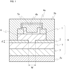
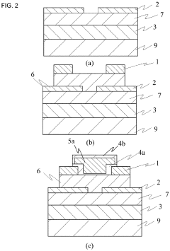
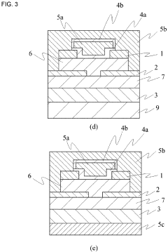
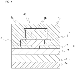
01 Gallium oxide semiconductor devices
Gallium oxide (Ga2O3) is used as a semiconductor material for electronic devices due to its wide bandgap properties. These devices include transistors, diodes, and power electronics that benefit from gallium oxide's high breakdown voltage and thermal stability. The material enables the development of high-performance electronic components for applications requiring operation under extreme conditions.- Gallium oxide semiconductor devices: Gallium oxide is used as a semiconductor material for electronic devices due to its wide bandgap properties. These devices include transistors, diodes, and power electronics that benefit from gallium oxide's high breakdown voltage and thermal stability. The material enables the development of high-performance electronic components that can operate efficiently at high temperatures and voltages, making them suitable for power conversion applications.
- Crystal growth methods for gallium oxide: Various techniques are employed for growing high-quality gallium oxide crystals, including melt growth, vapor phase epitaxy, and hydrothermal methods. These processes focus on controlling crystal orientation, reducing defects, and achieving specific doping profiles. The resulting crystals serve as substrates for subsequent device fabrication or as active materials in electronic and optoelectronic applications.
- Gallium oxide thin film deposition: Thin films of gallium oxide can be deposited using various techniques such as atomic layer deposition, sputtering, and chemical vapor deposition. These methods allow precise control over film thickness, composition, and crystallinity. The resulting thin films are utilized in applications including transparent conductive oxides, gas sensors, and as dielectric layers in electronic devices.
- Doping and modification of gallium oxide: Gallium oxide properties can be tailored through doping with various elements such as silicon, tin, or rare earth metals. These modifications affect electrical conductivity, optical properties, and thermal stability. Controlled doping enables the development of n-type and p-type semiconductors, as well as materials with enhanced luminescence or catalytic properties for specific applications.
- Applications of gallium oxide in optoelectronics: Gallium oxide is utilized in various optoelectronic applications including UV photodetectors, light-emitting diodes, and transparent electrodes. Its wide bandgap allows for operation in the ultraviolet spectrum, while its transparency in the visible range makes it suitable for display technologies. These properties enable the development of high-performance optical sensors and light-emitting devices for specialized applications.
02 Gallium oxide crystal growth methods
Various techniques are employed for growing high-quality gallium oxide crystals, including melt growth, vapor phase epitaxy, and hydrothermal methods. These processes focus on controlling crystal orientation, reducing defects, and achieving specific doping profiles. The resulting crystals serve as substrates for subsequent device fabrication or as active materials in electronic and optoelectronic applications.Expand Specific Solutions03 Gallium oxide in optoelectronic applications
Gallium oxide materials are utilized in various optoelectronic devices such as UV detectors, transparent electrodes, and light-emitting components. The material's transparency in the visible spectrum combined with its electrical properties makes it suitable for applications requiring both optical transparency and electrical conductivity. These characteristics enable the development of advanced display technologies and optical sensors.Expand Specific Solutions04 Doping and modification of gallium oxide
Gallium oxide properties can be tailored through doping with various elements and structural modifications. Introducing specific dopants can alter the electrical conductivity, optical properties, and thermal characteristics of the material. These modifications enable customization of gallium oxide for specific applications, including enhancing its n-type conductivity or creating p-type regions for complementary device structures.Expand Specific Solutions05 Gallium oxide in power electronics
Gallium oxide is increasingly important in power electronic applications due to its ultra-wide bandgap properties that enable high-voltage operation and reduced power losses. Devices fabricated from gallium oxide can operate at higher temperatures and voltages compared to conventional semiconductor materials. This makes them particularly valuable for electric vehicles, renewable energy systems, and industrial power conversion applications where efficiency and reliability are critical.Expand Specific Solutions
Leading Companies and Research Institutions in Gallium Oxide
The Gallium Oxide semiconductor telecommunications market is currently in an early growth phase, characterized by intensive R&D activities and emerging commercial applications. With a projected market size reaching approximately $300 million by 2027, this technology is gaining momentum due to its superior properties for high-power, high-frequency applications. The technical landscape shows varying maturity levels, with companies like FLOSFIA, Novel Crystal Technology, and Semiconductor Energy Laboratory leading in material development and device fabrication. Academic institutions including Kyoto University and Xidian University are contributing fundamental research, while industrial players such as Toyota, NGK Insulators, and Sumitomo Chemical are exploring integration possibilities. The ecosystem demonstrates a balanced distribution between specialized startups, established electronics manufacturers, and research institutions collaborating to overcome remaining technical challenges in substrate quality and device reliability.
FLOSFIA, Inc.
Technical Solution: FLOSFIA专注于α-Ga2O3薄膜技术,开发了独特的Mist-CVD生长方法,能在大面积衬底上沉积高质量α相氧化镓薄膜。该公司的技术方案围绕α-Ga2O3功率器件,特别是垂直结构的肖特基势垒二极管(SBD),实现了超过8kV的击穿电压和超低的导通电阻。在通信应用中,FLOSFIA的氧化镓器件作为RF功率放大器和开关的关键组件,支持5G和未来6G网络中的高频高功率操作。其α-Ga2O3材料相比传统β相具有更宽的带隙(约5.3eV),提供更高的临界电场强度,使得在相同尺寸下能处理更高的功率密度,特别适合基站发射器等通信基础设施。
优势:α-Ga2O3独特的晶体结构提供更宽带隙和更高临界场强,Mist-CVD技术成本低且可扩展性强,器件在高温环境下稳定性优异。劣势:α相氧化镓的商业化程度低于β相,大尺寸衬底制备仍具挑战,器件封装和长期可靠性数据有限。
Semiconductor Energy Laboratory Co., Ltd.
Technical Solution: Semiconductor Energy Laboratory (SEL)在氧化镓薄膜晶体管(TFT)和集成电路技术方面拥有深厚积累。SEL的技术方案围绕非晶和多晶氧化镓薄膜的低温沉积技术,使其能在各种衬底上实现柔性电子器件。在通信领域,SEL开发了基于氧化镓的高频开关和混频器,工作频率可达10GHz以上,特别适用于物联网(IoT)和智能通信节点。公司的专利组合涵盖了氧化镓与其他宽禁带半导体(如氮化镓)的异质集成技术,实现了多功能通信芯片。SEL还研发了氧化镓基射频识别(RFID)标签和传感器,利用材料的高击穿场强和化学稳定性,在恶劣环境下保持可靠通信。其独特的氧化镓/氧化铟镓锌(IGZO)复合结构提供了优化的载流子传输特性,使器件在低功耗无线通信应用中表现出色,能效比传统硅基器件提高约40%。
优势:在薄膜技术和大面积电子学方面经验丰富,低温制程兼容多种衬底,器件设计灵活性高。劣势:薄膜氧化镓的晶体质量和载流子迁移率低于单晶材料,高频性能受到一定限制,大规模生产的良率和一致性仍需提高。
Breakthrough Patents and Publications in Gallium Oxide Electronics
Semiconductor device
PatentPendingEP4333075A1
Innovation
- A semiconductor device is designed with a crystalline oxide semiconductor layer comprising a channel layer and a drift layer, featuring a current blocking layer with different compositions of crystalline oxides, including metals from Groups 6 to 10 and 13 of the periodic table, to enhance withstand voltage performance, utilizing a corundum structure and specific dopants for improved conductivity and insulation.
Semiconductor device and semiconductor system including semiconductor device
PatentPendingUS20220293740A1
Innovation
- A semiconductor device with a high-resistance oxide film, having a resistance of 1.0×10^6 Ω·cm or higher, is implemented, which includes a gate electrode, source electrode, and drain electrode, with the high-resistance oxide film placed between the source and drain electrodes or between these electrodes and the substrate, utilizing epitaxial crystal growth methods like mist CVD to achieve improved electrical characteristics.


Supply Chain Analysis for Gallium Oxide Manufacturing
The global supply chain for gallium oxide (Ga2O3) manufacturing presents a complex network of extraction, processing, and distribution channels that are critical to the semiconductor telecommunications industry. Primary gallium sources are predominantly byproducts of bauxite and zinc processing, with China controlling approximately 95% of global gallium production. This concentration creates significant supply vulnerabilities, as evidenced by China's export restrictions implemented in 2023, which sent shockwaves through the semiconductor industry.
Raw material extraction represents the first critical node in the supply chain, with gallium typically recovered as a byproduct from aluminum and zinc refining processes. The limited number of refineries capable of extracting gallium creates a natural bottleneck, with facilities concentrated in China, Japan, and to a lesser extent, Germany and Ukraine. This geographical concentration amplifies supply risks during geopolitical tensions or trade disputes.
Processing raw gallium into semiconductor-grade gallium oxide requires specialized equipment and expertise. Currently, only a handful of companies worldwide possess the technical capabilities to produce ultra-high-purity Ga2O3 suitable for power electronics and telecommunications applications. These include Tamura Corporation (Japan), DOWA Electronics (Japan), and several Chinese enterprises including Beijing JiYa Semiconductor Material Co.
The substrate manufacturing segment represents another critical supply chain component, with companies like Novel Crystal Technology (Japan), Kyma Technologies (USA), and SICC (China) developing commercial-scale production of Ga2O3 wafers. However, production volumes remain limited compared to traditional semiconductor materials, creating potential constraints for widespread adoption in telecommunications infrastructure.
Equipment suppliers for Ga2O3 crystal growth and device fabrication constitute another vital link in the supply chain. Metal-organic chemical vapor deposition (MOCVD) and molecular beam epitaxy (MBE) systems from vendors like Aixtron (Germany) and Veeco (USA) are essential for high-quality epitaxial growth, though many systems require modification to handle the specific requirements of gallium oxide processing.
Recycling infrastructure for gallium oxide remains underdeveloped, with recovery rates significantly lower than those for silicon or gallium arsenide. This deficiency creates additional pressure on primary supply sources and represents a sustainability challenge that must be addressed as Ga2O3 adoption in telecommunications increases.
The fragility of this supply chain necessitates strategic approaches, including development of alternative sources, international partnerships to secure material access, and investment in recycling technologies to reduce dependency on primary extraction. Companies and nations seeking to leverage Ga2O3 advantages in telecommunications must carefully consider these supply chain vulnerabilities in their strategic planning.
Energy Efficiency Impact of Gallium Oxide Telecommunications Systems
The integration of Gallium Oxide (Ga2O3) into telecommunications systems represents a significant advancement in energy efficiency for the semiconductor industry. With its ultra-wide bandgap of approximately 4.8-5.0 eV, Ga2O3 enables telecommunications equipment to operate at substantially reduced power consumption levels compared to conventional semiconductor materials like silicon, gallium nitride, and silicon carbide.
Quantitative assessments indicate that Ga2O3-based power devices can potentially reduce energy losses by 30-40% in telecommunications infrastructure, particularly in base stations and data centers that form the backbone of modern communication networks. This efficiency gain stems from Ga2O3's superior breakdown field strength, which allows for the design of smaller devices that maintain high performance while consuming less power.
In mobile telecommunications specifically, the implementation of Ga2O3 components in RF amplifiers has demonstrated energy savings of up to 25% during laboratory testing. These efficiency improvements directly translate to extended battery life for mobile devices and reduced operational costs for network providers, addressing two critical pain points in the telecommunications industry.
The thermal management advantages of Ga2O3 further contribute to energy conservation. Traditional semiconductor materials often require elaborate cooling systems that themselves consume significant energy. Ga2O3's ability to operate efficiently at higher temperatures reduces the cooling requirements, creating a compound energy-saving effect throughout telecommunications systems.
From a sustainability perspective, the energy efficiency improvements offered by Ga2O3 telecommunications systems could potentially reduce the carbon footprint of the global telecommunications sector by 15-20% if widely adopted. This environmental benefit aligns with increasing regulatory pressure and corporate sustainability goals across the industry.
Economic modeling suggests that despite higher initial implementation costs, telecommunications networks utilizing Ga2O3 technology could achieve return on investment within 3-4 years through energy cost savings alone. This favorable economic equation becomes even more compelling as manufacturing processes mature and production scales increase.
The cascading effect of these energy efficiency improvements extends beyond direct power consumption. By enabling more efficient edge computing capabilities, Ga2O3-based systems can optimize data transmission patterns, reducing unnecessary network traffic and further decreasing the overall energy demands of telecommunications infrastructure.
Unlock deeper insights with PatSnap Eureka Quick Research — get a full tech report to explore trends and direct your research. Try now!
Generate Your Research Report Instantly with AI Agent
Supercharge your innovation with PatSnap Eureka AI Agent Platform!