

High-k Dielectrics: Design Optimization for Power Electronics
MAY 13, 20268 MIN READ
Generate Your Research Report Instantly with AI Agent
PatSnap Eureka helps you evaluate technical feasibility & market potential.
High-k Dielectric Development Background and Power Electronics Goals
High-k dielectric materials have emerged as a critical technology frontier in the evolution of power electronics, driven by the fundamental need to overcome the limitations of conventional silicon dioxide and other traditional dielectric materials. The development trajectory of high-k dielectrics began in the semiconductor industry during the early 2000s, primarily addressing the scaling challenges in CMOS technology where gate oxide thickness approached atomic dimensions, leading to excessive leakage currents and reliability concerns.
The transition from traditional dielectrics to high-k materials represents a paradigm shift in material science and device engineering. Early research focused on materials such as hafnium oxide, zirconium oxide, and various perovskite structures, which demonstrated significantly higher dielectric constants while maintaining reasonable electrical properties. This foundational work established the theoretical framework and processing methodologies that would later be adapted for power electronics applications.
Power electronics applications present unique challenges that distinguish them from traditional semiconductor devices. The operating environment demands materials capable of withstanding high voltages, elevated temperatures, and rapid switching frequencies while maintaining low losses and high reliability. These requirements have driven the evolution of high-k dielectrics toward specialized compositions and structures optimized for power conversion systems, motor drives, renewable energy inverters, and electric vehicle power trains.
The primary technological objectives in high-k dielectric development for power electronics center on achieving superior breakdown voltage characteristics, minimizing dielectric losses across wide frequency ranges, and ensuring thermal stability under extreme operating conditions. Modern power systems require dielectric materials that can support voltage levels exceeding several kilovolts while maintaining compact form factors and high power density.
Contemporary research efforts focus on engineering materials with dielectric constants ranging from 20 to over 1000, depending on the specific application requirements. The goal extends beyond simply maximizing the dielectric constant to optimizing the balance between high permittivity, low loss tangent, high breakdown strength, and long-term reliability. Advanced material systems incorporating nanostructured composites, multilayer architectures, and functionally graded compositions represent the current state-of-the-art approaches.
The strategic importance of high-k dielectrics in power electronics continues to grow as global energy efficiency standards become more stringent and the demand for compact, high-performance power conversion systems increases across automotive, industrial, and renewable energy sectors.
The transition from traditional dielectrics to high-k materials represents a paradigm shift in material science and device engineering. Early research focused on materials such as hafnium oxide, zirconium oxide, and various perovskite structures, which demonstrated significantly higher dielectric constants while maintaining reasonable electrical properties. This foundational work established the theoretical framework and processing methodologies that would later be adapted for power electronics applications.
Power electronics applications present unique challenges that distinguish them from traditional semiconductor devices. The operating environment demands materials capable of withstanding high voltages, elevated temperatures, and rapid switching frequencies while maintaining low losses and high reliability. These requirements have driven the evolution of high-k dielectrics toward specialized compositions and structures optimized for power conversion systems, motor drives, renewable energy inverters, and electric vehicle power trains.
The primary technological objectives in high-k dielectric development for power electronics center on achieving superior breakdown voltage characteristics, minimizing dielectric losses across wide frequency ranges, and ensuring thermal stability under extreme operating conditions. Modern power systems require dielectric materials that can support voltage levels exceeding several kilovolts while maintaining compact form factors and high power density.
Contemporary research efforts focus on engineering materials with dielectric constants ranging from 20 to over 1000, depending on the specific application requirements. The goal extends beyond simply maximizing the dielectric constant to optimizing the balance between high permittivity, low loss tangent, high breakdown strength, and long-term reliability. Advanced material systems incorporating nanostructured composites, multilayer architectures, and functionally graded compositions represent the current state-of-the-art approaches.
The strategic importance of high-k dielectrics in power electronics continues to grow as global energy efficiency standards become more stringent and the demand for compact, high-performance power conversion systems increases across automotive, industrial, and renewable energy sectors.
Market Demand Analysis for High-k Power Electronic Components
The global power electronics market is experiencing unprecedented growth driven by the accelerating transition toward renewable energy systems, electric vehicles, and energy-efficient industrial applications. High-k dielectric materials have emerged as critical enablers for next-generation power electronic devices, addressing the fundamental need for improved performance, miniaturization, and thermal management in high-voltage, high-frequency applications.
Electric vehicle adoption represents one of the most significant demand drivers for advanced high-k dielectric components. The automotive industry's shift toward electrification requires power conversion systems capable of handling higher voltages and switching frequencies while maintaining compact form factors. Wide bandgap semiconductors like silicon carbide and gallium nitride, which are increasingly deployed in EV powertrains, demand sophisticated dielectric materials that can withstand elevated electric fields and operating temperatures.
Renewable energy infrastructure development creates substantial market opportunities for high-k dielectric technologies. Solar inverters, wind turbine power converters, and grid-tied energy storage systems require robust dielectric materials capable of reliable operation under harsh environmental conditions. The growing emphasis on grid modernization and smart grid technologies further amplifies demand for high-performance power electronic components with superior dielectric properties.
Industrial automation and motor drive applications constitute another major market segment driving high-k dielectric demand. Manufacturing facilities worldwide are implementing variable frequency drives and advanced motor control systems to improve energy efficiency and operational flexibility. These applications require dielectric materials that can maintain stable performance across wide temperature ranges while providing excellent insulation properties.
Data center power management represents an emerging high-growth application area. The exponential increase in cloud computing and artificial intelligence workloads necessitates highly efficient power delivery systems. High-k dielectric materials enable the development of compact, high-efficiency power converters essential for modern data center infrastructure.
Market dynamics indicate strong preference for dielectric solutions offering enhanced breakdown voltage, reduced leakage current, and improved thermal stability. End-users increasingly prioritize components that enable system-level benefits including reduced size, weight, and overall system cost while maintaining reliability standards required for mission-critical applications across automotive, industrial, and energy sectors.
Electric vehicle adoption represents one of the most significant demand drivers for advanced high-k dielectric components. The automotive industry's shift toward electrification requires power conversion systems capable of handling higher voltages and switching frequencies while maintaining compact form factors. Wide bandgap semiconductors like silicon carbide and gallium nitride, which are increasingly deployed in EV powertrains, demand sophisticated dielectric materials that can withstand elevated electric fields and operating temperatures.
Renewable energy infrastructure development creates substantial market opportunities for high-k dielectric technologies. Solar inverters, wind turbine power converters, and grid-tied energy storage systems require robust dielectric materials capable of reliable operation under harsh environmental conditions. The growing emphasis on grid modernization and smart grid technologies further amplifies demand for high-performance power electronic components with superior dielectric properties.
Industrial automation and motor drive applications constitute another major market segment driving high-k dielectric demand. Manufacturing facilities worldwide are implementing variable frequency drives and advanced motor control systems to improve energy efficiency and operational flexibility. These applications require dielectric materials that can maintain stable performance across wide temperature ranges while providing excellent insulation properties.
Data center power management represents an emerging high-growth application area. The exponential increase in cloud computing and artificial intelligence workloads necessitates highly efficient power delivery systems. High-k dielectric materials enable the development of compact, high-efficiency power converters essential for modern data center infrastructure.
Market dynamics indicate strong preference for dielectric solutions offering enhanced breakdown voltage, reduced leakage current, and improved thermal stability. End-users increasingly prioritize components that enable system-level benefits including reduced size, weight, and overall system cost while maintaining reliability standards required for mission-critical applications across automotive, industrial, and energy sectors.
Current Status and Challenges of High-k Dielectric Materials
High-k dielectric materials have emerged as critical components in modern power electronics, yet their widespread adoption faces significant technical and manufacturing challenges. Current high-k materials, including hafnium oxide (HfO2), zirconium oxide (ZrO2), and various perovskite structures, demonstrate promising dielectric constants ranging from 20 to over 100, substantially higher than traditional silicon dioxide. However, these materials often suffer from reliability issues, including charge trapping, interface instability, and degradation under high electric fields typical in power electronics applications.
The primary challenge lies in achieving the optimal balance between high dielectric constant and electrical stability. Many high-k materials exhibit significant leakage currents due to defect states within the bandgap, which compromise their insulating properties. Interface engineering between high-k dielectrics and semiconductor substrates remains problematic, with issues such as interdiffusion, formation of unwanted interfacial layers, and lattice mismatch leading to stress-induced defects. These interface challenges are particularly acute in wide bandgap semiconductors like silicon carbide and gallium nitride, which are increasingly important for power electronics.
Thermal stability represents another critical constraint, as power electronics operate under elevated temperatures that can trigger phase transitions in high-k materials, altering their dielectric properties. The crystalline-to-amorphous transitions observed in materials like HfO2 at processing temperatures above 400°C significantly impact device performance and long-term reliability.
Manufacturing scalability poses additional challenges, with many high-k deposition techniques requiring precise control of stoichiometry, crystalline structure, and thickness uniformity. Atomic layer deposition, while offering excellent conformality and thickness control, faces throughput limitations for large-scale production. Chemical vapor deposition methods often struggle with precursor chemistry and contamination issues that affect material purity and electrical properties.
Current research efforts focus on addressing these challenges through compositional engineering, including doping strategies to stabilize desired crystal phases and reduce defect densities. Multi-layer approaches combining different high-k materials aim to optimize both dielectric performance and interface quality, while novel deposition techniques seek to improve manufacturing feasibility and cost-effectiveness for power electronics applications.
The primary challenge lies in achieving the optimal balance between high dielectric constant and electrical stability. Many high-k materials exhibit significant leakage currents due to defect states within the bandgap, which compromise their insulating properties. Interface engineering between high-k dielectrics and semiconductor substrates remains problematic, with issues such as interdiffusion, formation of unwanted interfacial layers, and lattice mismatch leading to stress-induced defects. These interface challenges are particularly acute in wide bandgap semiconductors like silicon carbide and gallium nitride, which are increasingly important for power electronics.
Thermal stability represents another critical constraint, as power electronics operate under elevated temperatures that can trigger phase transitions in high-k materials, altering their dielectric properties. The crystalline-to-amorphous transitions observed in materials like HfO2 at processing temperatures above 400°C significantly impact device performance and long-term reliability.
Manufacturing scalability poses additional challenges, with many high-k deposition techniques requiring precise control of stoichiometry, crystalline structure, and thickness uniformity. Atomic layer deposition, while offering excellent conformality and thickness control, faces throughput limitations for large-scale production. Chemical vapor deposition methods often struggle with precursor chemistry and contamination issues that affect material purity and electrical properties.
Current research efforts focus on addressing these challenges through compositional engineering, including doping strategies to stabilize desired crystal phases and reduce defect densities. Multi-layer approaches combining different high-k materials aim to optimize both dielectric performance and interface quality, while novel deposition techniques seek to improve manufacturing feasibility and cost-effectiveness for power electronics applications.
Current High-k Dielectric Design Solutions
01 High-k dielectric materials and compositions
Development of high dielectric constant materials for electronic applications, including metal oxides, ceramic compositions, and composite materials that exhibit superior dielectric properties. These materials are designed to provide enhanced capacitance and electrical performance in various electronic devices and components.- High-k dielectric materials and compositions: Development of high dielectric constant materials for electronic applications, including metal oxides, ceramic compositions, and composite materials that exhibit superior dielectric properties. These materials are designed to provide enhanced capacitance and electrical performance in various electronic devices and components.
- Deposition and fabrication methods for high-k dielectric layers: Techniques for depositing and forming high-k dielectric layers on substrates, including chemical vapor deposition, atomic layer deposition, and sputtering methods. These processes enable precise control of layer thickness, uniformity, and interface properties for optimal device performance.
- Integration of high-k dielectrics in semiconductor devices: Methods for incorporating high-k dielectric materials into semiconductor device structures, including transistors, capacitors, and memory devices. The integration involves addressing interface compatibility, thermal stability, and electrical characteristics to achieve improved device performance and miniaturization.
- Surface treatment and interface engineering: Techniques for modifying surfaces and interfaces to optimize the performance of high-k dielectric materials, including surface passivation, interface layer formation, and chemical treatments. These methods help reduce interface defects and improve electrical properties of the dielectric stack.
- Characterization and testing of high-k dielectric properties: Methods and systems for measuring and evaluating the electrical, physical, and chemical properties of high-k dielectric materials, including capacitance measurements, leakage current analysis, and reliability testing. These characterization techniques ensure quality control and performance validation of dielectric materials.
02 Deposition and fabrication methods for high-k dielectric layers
Various techniques for depositing and forming high-k dielectric layers, including chemical vapor deposition, atomic layer deposition, and sputtering methods. These processes enable precise control over layer thickness, uniformity, and interface properties to achieve optimal dielectric performance in semiconductor devices.Expand Specific Solutions03 Integration of high-k dielectrics in semiconductor devices
Methods for incorporating high-k dielectric materials into transistors, capacitors, and memory devices to improve electrical characteristics and device performance. This includes gate dielectric applications, capacitor structures, and interface engineering to minimize leakage current and enhance reliability.Expand Specific Solutions04 Surface treatment and interface optimization
Techniques for treating surfaces and optimizing interfaces between high-k dielectric materials and substrates to improve adhesion, reduce defects, and enhance electrical properties. These methods include surface cleaning, passivation treatments, and barrier layer formation to ensure stable device operation.Expand Specific Solutions05 Characterization and testing of high-k dielectric properties
Methods and systems for measuring and evaluating the electrical, physical, and chemical properties of high-k dielectric materials. This includes techniques for determining dielectric constant, breakdown voltage, leakage current, and reliability parameters to ensure material quality and device performance.Expand Specific Solutions
Core High-k Material Innovation and Patent Analysis
Method and composition for fabricating a high-k dielectric material
PatentPendingIN201941047909A
Innovation
- A method involving the preparation of a solution by dispersing zirconium oxynitrate and lanthanum chloride, mixing with tetraethyl orthosilicate and titanium tetraisopropoxide, sonicating to form a colloidal gel, washing, drying, and heat-treating to obtain a solid powder, which is then spin-coated and annealed on an ITO glass substrate to reduce porosity and dielectric loss.


Method for integrating high-k dielectrics in transistor devices
PatentInactiveUS7045431B2
Innovation
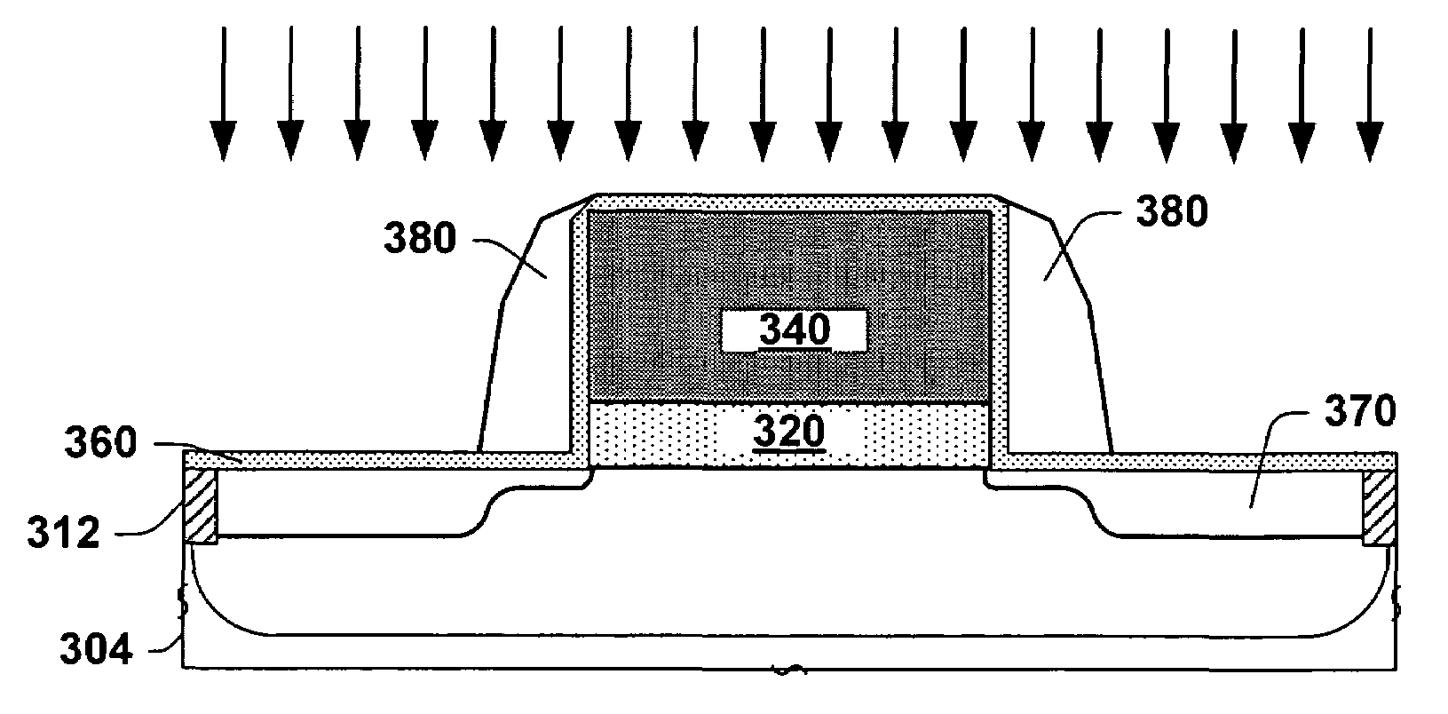
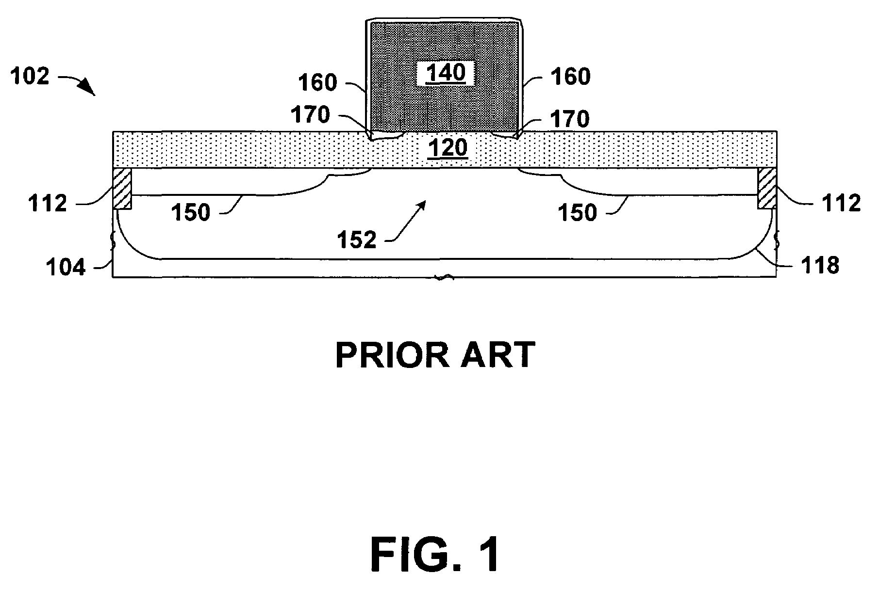
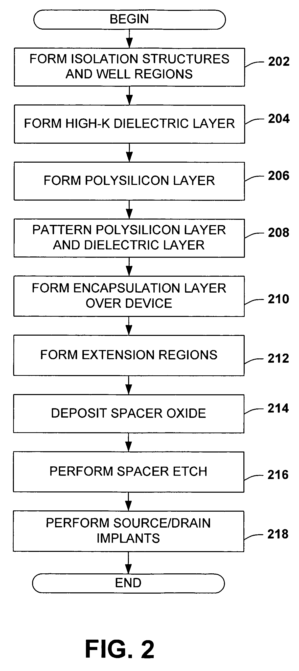
- The method involves forming high-k dielectric layers over semiconductor substrates and encapsulating exposed portions with a protective layer, which also serves as an etch stop and sidewall spacer, to mitigate defects and contamination, allowing for more uniform equivalent oxide thickness and improved device performance.

Environmental Impact Assessment of High-k Manufacturing
The manufacturing of high-k dielectric materials for power electronics applications presents significant environmental challenges that require comprehensive assessment and mitigation strategies. The production processes typically involve complex chemical synthesis routes, high-temperature processing, and the use of rare earth elements, all of which contribute to substantial environmental footprints across multiple impact categories.
Energy consumption represents one of the most critical environmental concerns in high-k dielectric manufacturing. The synthesis of materials such as hafnium oxide, zirconium oxide, and tantalum pentoxide requires temperatures exceeding 1000°C for extended periods, resulting in substantial carbon emissions. Advanced manufacturing facilities consume approximately 15-25 MWh per kilogram of processed high-k material, with associated CO2 emissions ranging from 8-12 tons per kilogram depending on the energy source composition.
Chemical waste generation poses another significant environmental challenge, particularly during the atomic layer deposition and chemical vapor deposition processes commonly used for high-k film formation. Precursor chemicals such as tetrakis(dimethylamido)hafnium and hafnium tetrachloride generate toxic byproducts including hydrochloric acid and organic amine compounds. Waste treatment systems must handle approximately 2-3 liters of chemical waste per square meter of processed substrate, requiring specialized neutralization and disposal protocols.
Water resource impact assessment reveals substantial consumption patterns, with manufacturing facilities typically requiring 500-800 liters of ultrapure water per kilogram of high-k material produced. The water treatment and purification processes generate secondary waste streams containing fluoride compounds and heavy metal residues, necessitating advanced treatment technologies before discharge or recycling.
Raw material extraction impacts extend beyond direct manufacturing, particularly for hafnium and tantalum sourcing. These materials often originate from conflict-sensitive regions, with mining operations generating significant land disturbance and ecosystem disruption. Life cycle assessments indicate that raw material extraction contributes 30-40% of the total environmental impact for high-k dielectric production chains.
Emerging mitigation strategies focus on process optimization and circular economy principles. Advanced plasma-enhanced deposition techniques can reduce processing temperatures by 200-300°C, potentially decreasing energy consumption by 25-35%. Solvent recovery systems and closed-loop chemical recycling can reduce waste generation by up to 60%, while alternative precursor chemistries based on less toxic compounds show promise for reducing hazardous waste streams.
Energy consumption represents one of the most critical environmental concerns in high-k dielectric manufacturing. The synthesis of materials such as hafnium oxide, zirconium oxide, and tantalum pentoxide requires temperatures exceeding 1000°C for extended periods, resulting in substantial carbon emissions. Advanced manufacturing facilities consume approximately 15-25 MWh per kilogram of processed high-k material, with associated CO2 emissions ranging from 8-12 tons per kilogram depending on the energy source composition.
Chemical waste generation poses another significant environmental challenge, particularly during the atomic layer deposition and chemical vapor deposition processes commonly used for high-k film formation. Precursor chemicals such as tetrakis(dimethylamido)hafnium and hafnium tetrachloride generate toxic byproducts including hydrochloric acid and organic amine compounds. Waste treatment systems must handle approximately 2-3 liters of chemical waste per square meter of processed substrate, requiring specialized neutralization and disposal protocols.
Water resource impact assessment reveals substantial consumption patterns, with manufacturing facilities typically requiring 500-800 liters of ultrapure water per kilogram of high-k material produced. The water treatment and purification processes generate secondary waste streams containing fluoride compounds and heavy metal residues, necessitating advanced treatment technologies before discharge or recycling.
Raw material extraction impacts extend beyond direct manufacturing, particularly for hafnium and tantalum sourcing. These materials often originate from conflict-sensitive regions, with mining operations generating significant land disturbance and ecosystem disruption. Life cycle assessments indicate that raw material extraction contributes 30-40% of the total environmental impact for high-k dielectric production chains.
Emerging mitigation strategies focus on process optimization and circular economy principles. Advanced plasma-enhanced deposition techniques can reduce processing temperatures by 200-300°C, potentially decreasing energy consumption by 25-35%. Solvent recovery systems and closed-loop chemical recycling can reduce waste generation by up to 60%, while alternative precursor chemistries based on less toxic compounds show promise for reducing hazardous waste streams.
Reliability and Safety Standards for High-k Power Devices
The reliability and safety standards for high-k power devices represent a critical framework governing the deployment of advanced dielectric materials in power electronics applications. These standards encompass comprehensive testing protocols, performance benchmarks, and safety requirements that ensure consistent operation under extreme electrical, thermal, and mechanical stress conditions.
International standards organizations, including IEC, IEEE, and JEDEC, have established specific guidelines for high-k dielectric materials used in power semiconductor devices. These standards define minimum breakdown voltage requirements, typically ranging from 10-50 MV/cm depending on the application, along with maximum allowable leakage current densities below 10^-6 A/cm² at operating voltages. Temperature cycling requirements mandate device functionality across -55°C to +175°C ranges, with some military applications extending to +200°C.
Accelerated life testing protocols form the backbone of reliability assessment for high-k power devices. Time-dependent dielectric breakdown (TDDB) testing evaluates long-term reliability under constant voltage stress, while temperature-humidity-bias (THB) testing assesses performance degradation under combined environmental stresses. These tests typically require 1000-hour minimum durations with failure rates below 100 FIT (Failures in Time) for commercial applications.
Safety standards specifically address electrical isolation requirements, mandating minimum creepage and clearance distances based on working voltages and pollution degrees. For high-voltage power modules incorporating high-k dielectrics, isolation voltage requirements often exceed 4000V RMS, with partial discharge inception voltages maintained above 1.5 times the working voltage to prevent long-term degradation.
Qualification standards also encompass electromagnetic compatibility (EMC) requirements, ensuring high-k power devices do not generate excessive electromagnetic interference while maintaining immunity to external disturbances. Power cycling capability standards require devices to withstand minimum 100,000 thermal cycles with junction temperature swings exceeding 100°C, validating the mechanical integrity of high-k dielectric layers under repeated thermal expansion and contraction.
International standards organizations, including IEC, IEEE, and JEDEC, have established specific guidelines for high-k dielectric materials used in power semiconductor devices. These standards define minimum breakdown voltage requirements, typically ranging from 10-50 MV/cm depending on the application, along with maximum allowable leakage current densities below 10^-6 A/cm² at operating voltages. Temperature cycling requirements mandate device functionality across -55°C to +175°C ranges, with some military applications extending to +200°C.
Accelerated life testing protocols form the backbone of reliability assessment for high-k power devices. Time-dependent dielectric breakdown (TDDB) testing evaluates long-term reliability under constant voltage stress, while temperature-humidity-bias (THB) testing assesses performance degradation under combined environmental stresses. These tests typically require 1000-hour minimum durations with failure rates below 100 FIT (Failures in Time) for commercial applications.
Safety standards specifically address electrical isolation requirements, mandating minimum creepage and clearance distances based on working voltages and pollution degrees. For high-voltage power modules incorporating high-k dielectrics, isolation voltage requirements often exceed 4000V RMS, with partial discharge inception voltages maintained above 1.5 times the working voltage to prevent long-term degradation.
Qualification standards also encompass electromagnetic compatibility (EMC) requirements, ensuring high-k power devices do not generate excessive electromagnetic interference while maintaining immunity to external disturbances. Power cycling capability standards require devices to withstand minimum 100,000 thermal cycles with junction temperature swings exceeding 100°C, validating the mechanical integrity of high-k dielectric layers under repeated thermal expansion and contraction.
Unlock deeper insights with PatSnap Eureka Quick Research — get a full tech report to explore trends and direct your research. Try now!
Generate Your Research Report Instantly with AI Agent
Supercharge your innovation with PatSnap Eureka AI Agent Platform!