

High-k Dielectrics vs SiC: Electronics Performance Evaluation
MAY 13, 20269 MIN READ
Generate Your Research Report Instantly with AI Agent
PatSnap Eureka helps you evaluate technical feasibility & market potential.
High-k Dielectrics and SiC Technology Background and Objectives
High-k dielectric materials and silicon carbide (SiC) semiconductors represent two pivotal technological domains that have fundamentally transformed modern electronics over the past two decades. High-k dielectrics emerged as a critical solution to address the scaling limitations of traditional silicon dioxide gate dielectrics in complementary metal-oxide-semiconductor (CMOS) technology. As transistor dimensions continued to shrink below 90nm technology nodes, conventional SiO2 gate dielectrics became impractically thin, leading to excessive gate leakage currents that compromised device performance and power efficiency.
The evolution of high-k dielectrics began with materials such as hafnium dioxide (HfO2), aluminum oxide (Al2O3), and various rare earth oxides, which offered dielectric constants significantly higher than SiO2's value of 3.9. These materials enabled the maintenance of equivalent electrical thickness while using physically thicker layers, thereby reducing quantum tunneling effects and gate leakage. The integration of high-k dielectrics with metal gate electrodes became standard practice in advanced CMOS processes, enabling continued Moore's Law scaling and improved transistor performance.
Simultaneously, silicon carbide technology has undergone remarkable advancement, transitioning from a niche wide-bandgap semiconductor to a mainstream solution for power electronics applications. SiC's superior material properties, including a bandgap of 3.3eV, high breakdown electric field strength exceeding 3MV/cm, and excellent thermal conductivity, position it as an ideal candidate for high-voltage, high-frequency, and high-temperature applications where silicon reaches its fundamental limits.
The convergence of these two technologies presents unprecedented opportunities for next-generation electronic devices. The primary objective of evaluating high-k dielectrics versus SiC lies in understanding their complementary roles in addressing different segments of the electronics market. While high-k dielectrics primarily enhance digital logic performance and enable continued CMOS scaling, SiC technology revolutionizes power conversion efficiency and enables new applications in electric vehicles, renewable energy systems, and industrial power management.
The technical objectives encompass comprehensive performance evaluation across multiple dimensions including electrical characteristics, thermal management, reliability, and manufacturing scalability. This evaluation aims to identify optimal application domains for each technology, potential synergies when combined, and future development pathways that could maximize their respective advantages in emerging electronic systems requiring both high computational performance and efficient power management capabilities.
Market Demand Analysis for Advanced Electronic Materials
The global semiconductor industry is experiencing unprecedented demand for advanced electronic materials, driven by the rapid expansion of high-performance computing, artificial intelligence, and next-generation communication technologies. This surge has created substantial market opportunities for both high-k dielectric materials and silicon carbide components, each addressing distinct performance requirements across various application segments.
High-k dielectric materials have emerged as critical enablers for continued semiconductor scaling, particularly in advanced logic and memory devices. The market demand stems primarily from the need to reduce gate leakage current while maintaining capacitance in increasingly miniaturized transistors. Major semiconductor manufacturers are actively seeking high-k solutions to replace traditional silicon dioxide in sub-nanometer process nodes, creating a robust demand base in the foundry and memory sectors.
Silicon carbide materials are experiencing explosive growth in power electronics applications, driven by the global transition toward electric vehicles, renewable energy systems, and energy-efficient industrial equipment. The automotive sector represents the largest demand driver, as electric vehicle manufacturers require power semiconductors capable of handling high voltages and temperatures while maintaining superior efficiency compared to traditional silicon-based solutions.
The telecommunications infrastructure modernization, particularly the deployment of 5G networks and edge computing facilities, has generated significant demand for both material categories. High-k dielectrics enable the high-frequency performance required in RF applications, while SiC components provide the power handling capabilities necessary for base station power amplifiers and switching systems.
Industrial automation and smart grid applications constitute another major demand segment, where the superior thermal properties and breakdown voltage characteristics of these advanced materials enable more compact and efficient power conversion systems. The growing emphasis on energy efficiency regulations across global markets has accelerated adoption rates in industrial power electronics.
Emerging applications in aerospace, defense, and space exploration are creating specialized demand for materials capable of operating under extreme conditions. Both high-k dielectrics and SiC materials offer enhanced radiation tolerance and temperature stability compared to conventional alternatives, making them essential for next-generation satellite systems and military electronics.
The market dynamics are further influenced by supply chain considerations, as manufacturers seek to diversify material sources and reduce dependency on traditional silicon-based solutions. This trend has intensified following recent global supply chain disruptions, creating additional momentum for advanced material adoption across multiple industry segments.
Current Status and Challenges in High-k and SiC Technologies
High-k dielectric materials have achieved significant commercial success in advanced semiconductor manufacturing, particularly in sub-22nm technology nodes. Leading foundries have successfully integrated hafnium-based high-k dielectrics with metal gates in their production lines, demonstrating excellent scalability and reliability. These materials effectively address the gate leakage issues that plagued traditional silicon dioxide dielectrics at reduced dimensions. Current high-k implementations show dielectric constants ranging from 20-25, enabling equivalent oxide thickness scaling while maintaining acceptable leakage current densities below 1×10⁻² A/cm².
Silicon carbide technology has matured substantially in power electronics applications, with 4H-SiC emerging as the dominant polytype for commercial devices. Major manufacturers have established robust 150mm wafer production capabilities, with 200mm wafer technology rapidly advancing. SiC power devices demonstrate superior performance in high-voltage, high-frequency applications, achieving breakdown voltages exceeding 10kV and operating frequencies above 100kHz with significantly reduced switching losses compared to silicon counterparts.
Despite these advances, both technologies face substantial technical challenges. High-k dielectrics suffer from mobility degradation due to increased interface scattering, with electron mobility reductions of 30-50% compared to SiO₂/Si interfaces. Threshold voltage instability and bias temperature instability remain persistent issues, particularly under high-field stress conditions. The integration complexity increases significantly when combining high-k materials with advanced channel materials beyond silicon.
SiC technology confronts manufacturing challenges including crystal defect density control, with basal plane dislocations and micropipe defects still limiting device yield and reliability. The SiC/SiO₂ interface quality remains inferior to Si/SiO₂, exhibiting higher interface trap densities that degrade MOSFET channel mobility. Processing temperatures exceeding 1600°C create additional manufacturing complexities and equipment requirements.
Cost considerations present ongoing challenges for both technologies. High-k dielectric integration requires sophisticated atomic layer deposition equipment and precise process control, increasing manufacturing costs. SiC substrate costs remain 5-10 times higher than silicon wafers of comparable size, though economies of scale are gradually reducing this premium. The specialized processing requirements for both technologies demand significant capital investments and technical expertise.
Reliability assessment reveals technology-specific concerns. High-k dielectrics show improved time-dependent dielectric breakdown characteristics but exhibit complex degradation mechanisms under electrical stress. SiC devices demonstrate excellent thermal stability and radiation hardness but face challenges with long-term reliability validation due to the technology's relative novelty in high-volume applications.
Current Technical Solutions for Electronic Performance Enhancement
01 High-k dielectric materials for gate applications
High-k dielectric materials are utilized in semiconductor devices to replace traditional silicon dioxide as gate dielectrics. These materials offer superior dielectric constants, enabling reduced gate leakage current and improved device scaling. The implementation of high-k dielectrics allows for thinner equivalent oxide thickness while maintaining electrical performance, which is crucial for advanced semiconductor manufacturing processes.- High-k dielectric materials for improved gate performance: High-k dielectric materials are utilized to enhance gate performance in semiconductor devices by providing superior dielectric properties compared to traditional silicon dioxide. These materials enable reduced gate leakage current, improved capacitance control, and enhanced device scaling capabilities. The implementation of high-k dielectrics allows for thinner equivalent oxide thickness while maintaining electrical performance.
- SiC-based electronic device structures and fabrication: Silicon carbide electronic devices demonstrate superior performance characteristics including high temperature operation, enhanced power handling capabilities, and improved switching speeds. The fabrication processes for SiC devices involve specialized techniques for crystal growth, doping control, and interface engineering to optimize electrical properties and device reliability.
- Dielectric layer integration in power semiconductor devices: Integration of advanced dielectric layers in power semiconductor applications focuses on optimizing breakdown voltage, reducing switching losses, and improving thermal management. These approaches involve careful selection of dielectric materials and their deposition methods to achieve desired electrical isolation and performance characteristics in high-power applications.
- Interface engineering between dielectrics and semiconductor substrates: Interface engineering techniques are employed to optimize the boundary between dielectric materials and semiconductor substrates, particularly focusing on reducing interface trap density, improving carrier mobility, and enhancing device reliability. These methods involve surface preparation, passivation techniques, and controlled deposition processes to achieve high-quality interfaces.
- Comparative performance analysis and optimization strategies: Performance comparison methodologies evaluate the effectiveness of different dielectric and semiconductor material combinations through electrical characterization, reliability testing, and thermal analysis. Optimization strategies focus on balancing trade-offs between electrical performance, manufacturing complexity, and cost considerations to achieve optimal device characteristics for specific applications.
02 SiC power device performance optimization
Silicon carbide electronics demonstrate superior performance characteristics including high breakdown voltage, thermal conductivity, and switching frequency capabilities. These properties make them particularly suitable for power electronics applications where efficiency and thermal management are critical. The wide bandgap nature of the material enables operation at higher temperatures and voltages compared to traditional silicon-based devices.Expand Specific Solutions03 Dielectric layer fabrication and processing techniques
Advanced fabrication methods for creating high-quality dielectric layers involve precise deposition techniques, annealing processes, and interface engineering. These manufacturing approaches focus on achieving optimal thickness control, minimizing defect density, and ensuring uniform electrical properties across the substrate. The processing parameters significantly influence the final device performance and reliability.Expand Specific Solutions04 Interface engineering between dielectrics and semiconductors
The interface quality between high-k dielectric materials and semiconductor substrates critically affects device performance. Interface engineering techniques include surface preparation, interlayer optimization, and defect passivation methods. These approaches aim to minimize interface trap density, reduce charge scattering, and improve carrier mobility while maintaining the desired electrical isolation properties.Expand Specific Solutions05 Comparative analysis of material properties and device integration
Systematic evaluation of different dielectric and semiconductor material combinations reveals trade-offs between electrical performance, thermal stability, and manufacturing complexity. The analysis encompasses dielectric constant values, breakdown field strength, thermal expansion matching, and processing compatibility. This comparative approach guides material selection for specific application requirements and performance targets.Expand Specific Solutions
Major Players in High-k Dielectrics and SiC Industry
The high-k dielectrics versus SiC electronics performance evaluation represents a mature technology landscape in the growth-to-maturity transition phase. The market demonstrates substantial scale, driven by increasing demand for advanced semiconductor solutions in automotive, power electronics, and high-frequency applications. Technology maturity varies significantly across players: established semiconductor giants like Intel, Samsung Electronics, TSMC, and Texas Instruments have achieved high maturity in high-k dielectric integration, while specialized SiC companies like GeneSiC Semiconductor focus on wide bandgap innovations. Equipment manufacturers including Tokyo Electron and foundries like GlobalFoundries provide critical infrastructure support. The competitive landscape shows clear segmentation between traditional silicon-based high-k solutions and emerging SiC technologies, with companies like ROHM, Fuji Electric, and NXP bridging both domains through diverse product portfolios targeting specific performance requirements.
Intel Corp.
Technical Solution: Intel has extensively developed high-k dielectric materials, particularly hafnium-based compounds (HfO2) integrated with metal gate technology for advanced CMOS processes. Their high-k/metal gate stack technology enables continued transistor scaling while maintaining low leakage current and high drive current. Intel's approach focuses on optimizing the interface between high-k dielectrics and silicon channels, achieving equivalent oxide thickness (EOT) below 1nm while managing threshold voltage control and mobility degradation issues. The company has also explored high-k materials for capacitor applications in memory devices.
Strengths: Industry-leading high-k dielectric integration, proven manufacturing scalability, strong interface engineering capabilities. Weaknesses: Limited SiC power device portfolio, primarily focused on silicon-based solutions, high development costs for new material systems.
Taiwan Semiconductor Manufacturing Co., Ltd.
Technical Solution: TSMC has developed comprehensive high-k dielectric solutions for advanced logic nodes, implementing hafnium-based high-k materials with metal gates across multiple process generations. Their technology platform includes optimized high-k stacks for both high-performance and low-power applications, with careful attention to work function engineering and interface optimization. TSMC's high-k implementation focuses on minimizing equivalent oxide thickness while controlling short-channel effects and maintaining reliability standards. The company has also begun exploring high-k materials for emerging applications including power management ICs.
Strengths: Advanced process technology leadership, excellent manufacturing yield control, comprehensive high-k material characterization. Weaknesses: Limited direct SiC manufacturing experience, primarily silicon-focused technology development, dependency on equipment supplier innovations.
Key Innovations in High-k Dielectrics and SiC Integration
Integrated dielectric and method
PatentInactiveUS20020025626A1
Innovation
- An ultra-thin monolayer of SiC is formed as a reaction barrier between the silicon substrate and the high-k dielectric, preventing the formation of a thick SiO2 layer and allowing for the deposition of high permittivity materials like Ta2O5, thereby maintaining capacitance density and device performance.


Method for integrating high-k dielectrics in transistor devices
PatentInactiveUS7045431B2
Innovation
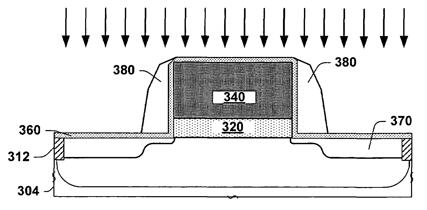
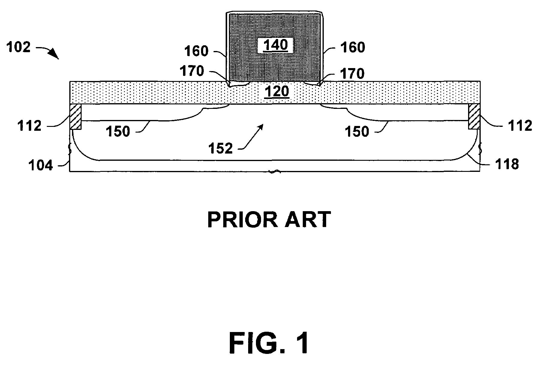
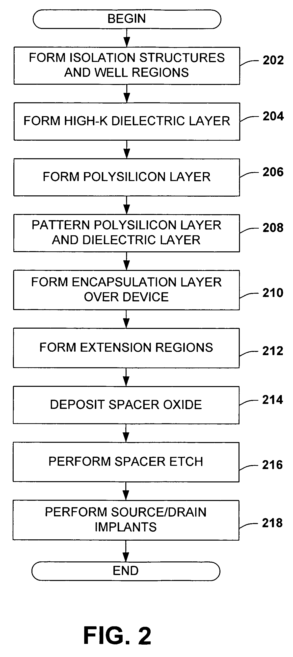
- The method involves forming high-k dielectric layers over semiconductor substrates and encapsulating exposed portions with a protective layer, which also serves as an etch stop and sidewall spacer, to mitigate defects and contamination, allowing for more uniform equivalent oxide thickness and improved device performance.

Manufacturing Process and Equipment Requirements Analysis
The manufacturing processes for high-k dielectrics and silicon carbide (SiC) semiconductors require fundamentally different approaches, equipment configurations, and process control methodologies. High-k dielectric materials, typically hafnium-based compounds like HfO2, demand atomic layer deposition (ALD) systems capable of precise thickness control at the nanometer scale. These systems operate under ultra-high vacuum conditions with temperatures ranging from 200-400°C, requiring specialized precursor delivery systems and purge gas management.
SiC manufacturing relies primarily on chemical vapor deposition (CVD) processes, particularly for epitaxial layer growth. The equipment must withstand significantly higher temperatures, often exceeding 1600°C, necessitating specialized heating elements, temperature control systems, and corrosion-resistant chamber materials. High-temperature furnaces with precise atmospheric control are essential for maintaining crystal quality and minimizing defect formation.
Equipment requirements differ substantially between these technologies. High-k dielectric processing demands cleanroom environments with Class 1 particulate control, sophisticated metrology tools for thickness measurement, and specialized etch chambers for pattern definition. The ALD reactors require multiple precursor lines, mass flow controllers, and advanced process monitoring systems to ensure uniform film deposition across large wafer surfaces.
SiC processing equipment must accommodate the material's chemical inertness and high melting point. Specialized grinding and polishing equipment is necessary for wafer preparation, while ion implantation systems require higher energy capabilities to achieve adequate dopant penetration. The epitaxial reactors need robust heating systems, typically using induction or resistance heating, along with precise gas flow control for maintaining stoichiometry.
Process integration challenges emerge when combining these materials in hybrid device architectures. Cross-contamination prevention becomes critical, requiring dedicated processing lines or extensive cleaning protocols between material transitions. Temperature cycling compatibility must be carefully managed, as the thermal expansion coefficients and processing temperatures differ significantly between high-k dielectrics and SiC substrates.
Quality control and metrology requirements vary considerably. High-k dielectric manufacturing relies heavily on ellipsometry, X-ray photoelectron spectroscopy, and capacitance-voltage measurements for film characterization. SiC processing emphasizes defect detection through photoluminescence mapping, minority carrier lifetime measurements, and high-resolution X-ray diffraction for crystal quality assessment.
Reliability and Thermal Management Considerations
Reliability considerations for high-k dielectrics and SiC-based electronic devices present distinct challenges that significantly impact long-term performance and operational stability. High-k dielectric materials, while offering superior capacitance density, face reliability concerns related to charge trapping, interface state generation, and dielectric breakdown under prolonged electrical stress. These materials exhibit time-dependent dielectric breakdown (TDDB) characteristics that differ substantially from traditional silicon dioxide, requiring extensive reliability testing protocols to establish operational lifetimes.
SiC devices demonstrate exceptional reliability advantages in high-temperature and high-voltage applications due to their inherent material properties. The wide bandgap nature of SiC provides superior resistance to thermal degradation and maintains stable electrical characteristics across extended temperature ranges. However, SiC reliability challenges primarily stem from interface quality between SiC and gate dielectrics, where defect states can impact device threshold voltage stability and create long-term drift phenomena.
Thermal management represents a critical differentiator between these technologies. High-k dielectrics typically exhibit lower thermal conductivity compared to SiO2, creating localized heating effects that can accelerate degradation mechanisms. The reduced thermal conductivity ranges from 1-3 W/mK for most high-k materials, compared to 1.4 W/mK for SiO2, potentially creating thermal bottlenecks in high-power applications.
SiC's superior thermal properties, including thermal conductivity of approximately 490 W/mK and operating temperature capabilities exceeding 200°C, provide significant advantages for thermal management. This enables more efficient heat dissipation and reduces the need for complex cooling systems, particularly beneficial in power electronics and automotive applications where thermal cycling and elevated operating temperatures are common.
The interaction between reliability and thermal management becomes particularly critical in mission-critical applications. High-k dielectric devices require careful thermal design considerations to prevent accelerated aging, while SiC devices can leverage their thermal robustness to achieve higher power densities and improved system-level reliability through reduced thermal stress on surrounding components.
Unlock deeper insights with PatSnap Eureka Quick Research — get a full tech report to explore trends and direct your research. Try now!
Generate Your Research Report Instantly with AI Agent
Supercharge your innovation with PatSnap Eureka AI Agent Platform!