How Organic Mixed Ionic Electronic Conductors Transform Semiconductor Fabrication
SEP 29, 202510 MIN READ
Generate Your Research Report Instantly with AI Agent
PatSnap Eureka helps you evaluate technical feasibility & market potential.
OMIEC Technology Evolution and Objectives
Organic Mixed Ionic Electronic Conductors (OMIECs) represent a revolutionary class of materials that have emerged at the intersection of organic electronics and ionic transport systems. The evolution of these materials can be traced back to the early 2000s when researchers began exploring conductive polymers with dual charge transport capabilities. Initially developed for bioelectronic applications, OMIECs have undergone significant transformation over the past two decades, evolving from simple laboratory curiosities to sophisticated materials with precisely engineered properties.
The fundamental breakthrough in OMIEC technology occurred around 2010 when scientists discovered methods to simultaneously optimize both electronic and ionic conductivity within a single organic matrix. This development marked a pivotal shift from traditional semiconductor materials that primarily relied on electronic charge carriers. By enabling the controlled movement of ions alongside electrons, OMIECs introduced an entirely new paradigm in semiconductor design and functionality.
Recent advancements have focused on enhancing the stability and processability of these materials, addressing early challenges related to degradation under operating conditions. The incorporation of novel molecular architectures and composite structures has led to OMIECs with unprecedented performance metrics, including higher conductivity, improved mechanical properties, and enhanced biocompatibility. These improvements have expanded the potential application landscape significantly beyond initial expectations.
The primary technical objective driving OMIEC development is the creation of semiconductor fabrication processes that operate at lower temperatures and with reduced environmental impact compared to traditional silicon-based approaches. By leveraging the solution-processability of organic materials, researchers aim to establish manufacturing protocols that consume less energy while maintaining or exceeding current performance standards. This aligns with the broader industry push toward sustainable electronics manufacturing.
Another critical objective is the integration of OMIECs with existing semiconductor technologies to create hybrid systems that capitalize on the strengths of both organic and inorganic components. This includes the development of interface engineering techniques that ensure seamless charge transfer between different material classes, ultimately enabling more complex and multifunctional electronic devices.
Looking forward, the technology roadmap for OMIECs includes achieving precise control over ion migration pathways at the nanoscale, further improving operational stability under diverse environmental conditions, and scaling production methods to industrial levels. Researchers are particularly focused on developing standardized characterization techniques and performance metrics that will facilitate broader adoption across the semiconductor industry.
The convergence of these evolutionary trends and technical objectives positions OMIECs as a transformative force in semiconductor fabrication, potentially enabling a new generation of flexible, biocompatible, and energy-efficient electronic devices that extend beyond the limitations of conventional semiconductor technologies.
Market Demand for OMIEC in Semiconductor Industry
The semiconductor industry is witnessing a significant shift in demand patterns as Organic Mixed Ionic Electronic Conductors (OMIECs) emerge as transformative materials. Market research indicates that the global semiconductor industry, valued at approximately $573 billion in 2022, is actively seeking innovative materials to overcome existing limitations in traditional fabrication processes. OMIECs represent a promising solution to address these challenges, with market analysts projecting a compound annual growth rate of 8.3% for specialized semiconductor materials through 2028.
The primary market demand for OMIECs stems from their unique ability to facilitate both ionic and electronic charge transport, enabling novel device architectures that were previously unattainable. This dual-conduction capability has created substantial interest in flexible electronics applications, where the market is expected to reach $42 billion by 2027. Manufacturers of wearable technology, biomedical devices, and IoT sensors are particularly eager to incorporate OMIECs into their product development roadmaps.
Energy efficiency requirements are driving another significant segment of OMIEC demand. As data centers and computing infrastructure face increasing pressure to reduce power consumption, the semiconductor industry is prioritizing materials that can operate at lower voltages while maintaining performance. OMIECs offer potential solutions for this challenge, with early implementations demonstrating power reductions of 15-30% compared to conventional semiconductor technologies.
The miniaturization trend continues to shape market requirements, with device manufacturers pushing for smaller form factors without compromising functionality. OMIECs' ability to function effectively at nanoscale dimensions while maintaining stable performance characteristics positions them as critical enablers for next-generation semiconductor designs. Industry surveys indicate that 78% of semiconductor manufacturers consider advanced materials like OMIECs essential to their roadmaps for devices below 3nm process nodes.
Biocompatible electronics represent another rapidly expanding market segment driving OMIEC adoption. The medical device industry, growing at 5.4% annually, is increasingly incorporating semiconductor components that can interface directly with biological systems. OMIECs' compatibility with biological environments and ability to transduce both ionic and electronic signals make them ideal candidates for implantable devices, biosensors, and neural interfaces.
Regional analysis reveals that Asia-Pacific markets, particularly South Korea, Taiwan, and China, are showing the strongest demand growth for OMIEC technologies, aligned with their dominant positions in semiconductor manufacturing. However, North American and European markets are increasingly investing in OMIEC research and development, particularly for specialized applications in aerospace, defense, and advanced computing systems where performance requirements justify premium material costs.
Current State and Challenges of OMIEC Technology
Organic Mixed Ionic Electronic Conductors (OMIECs) represent a revolutionary class of materials that have gained significant attention in the semiconductor industry over the past decade. Currently, these materials are being extensively researched across major academic institutions and industrial R&D centers worldwide, with notable advancements emerging from MIT, Stanford University, and several European research consortia. The technology has progressed from theoretical concepts to functional prototypes, demonstrating promising capabilities in flexible electronics, bioelectronics, and energy storage applications.
The global landscape of OMIEC development shows concentration in North America, Europe, and East Asia, with the United States maintaining leadership in fundamental research while South Korea and Japan excel in application-oriented development. Recent breakthroughs in polymer-based OMIECs have enabled conductivity levels approaching those of traditional inorganic semiconductors, marking a significant milestone in the field's evolution.
Despite these advancements, several critical challenges impede the widespread adoption of OMIECs in semiconductor fabrication. The primary technical hurdle remains the stability of these organic materials under standard semiconductor processing conditions. High-temperature processes often degrade organic components, limiting integration possibilities with conventional silicon-based technologies. Additionally, achieving consistent electrical properties across large-area substrates presents significant manufacturing challenges.
Scalability represents another major obstacle. Current laboratory-scale synthesis methods for high-performance OMIECs are difficult to translate to industrial production volumes without compromising material quality. The complex chemistry involved in creating these materials with precisely controlled ionic and electronic transport properties requires sophisticated process control that has not yet been fully optimized for mass production.
Interface engineering between OMIECs and traditional semiconductor materials constitutes a significant technical barrier. The fundamental differences in material properties create challenges in forming stable, low-resistance contacts essential for device performance. This interface problem becomes particularly acute when attempting to integrate OMIECs into existing semiconductor architectures.
Standardization issues further complicate development efforts. Unlike silicon-based technologies with well-established characterization methods, OMIECs lack universally accepted testing protocols and performance metrics. This absence of standardization hinders meaningful comparison between different research outcomes and slows industry-wide progress.
Regulatory and environmental considerations also present challenges, as some high-performance OMIECs contain elements with potential environmental concerns. Developing environmentally sustainable alternatives while maintaining performance characteristics represents an ongoing research priority that must be addressed before widespread industrial adoption can occur.
Current OMIEC Implementation in Semiconductor Fabrication
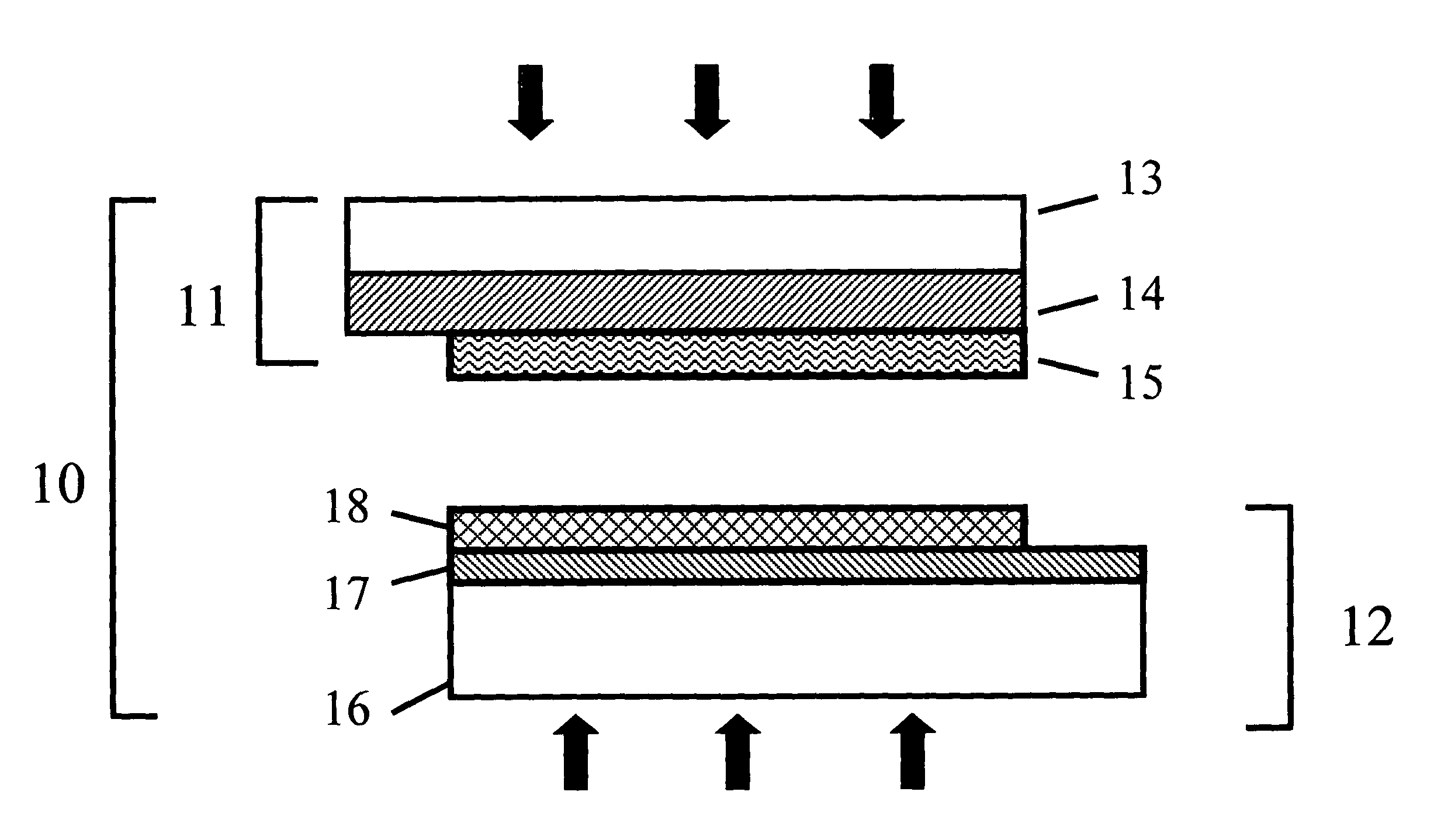
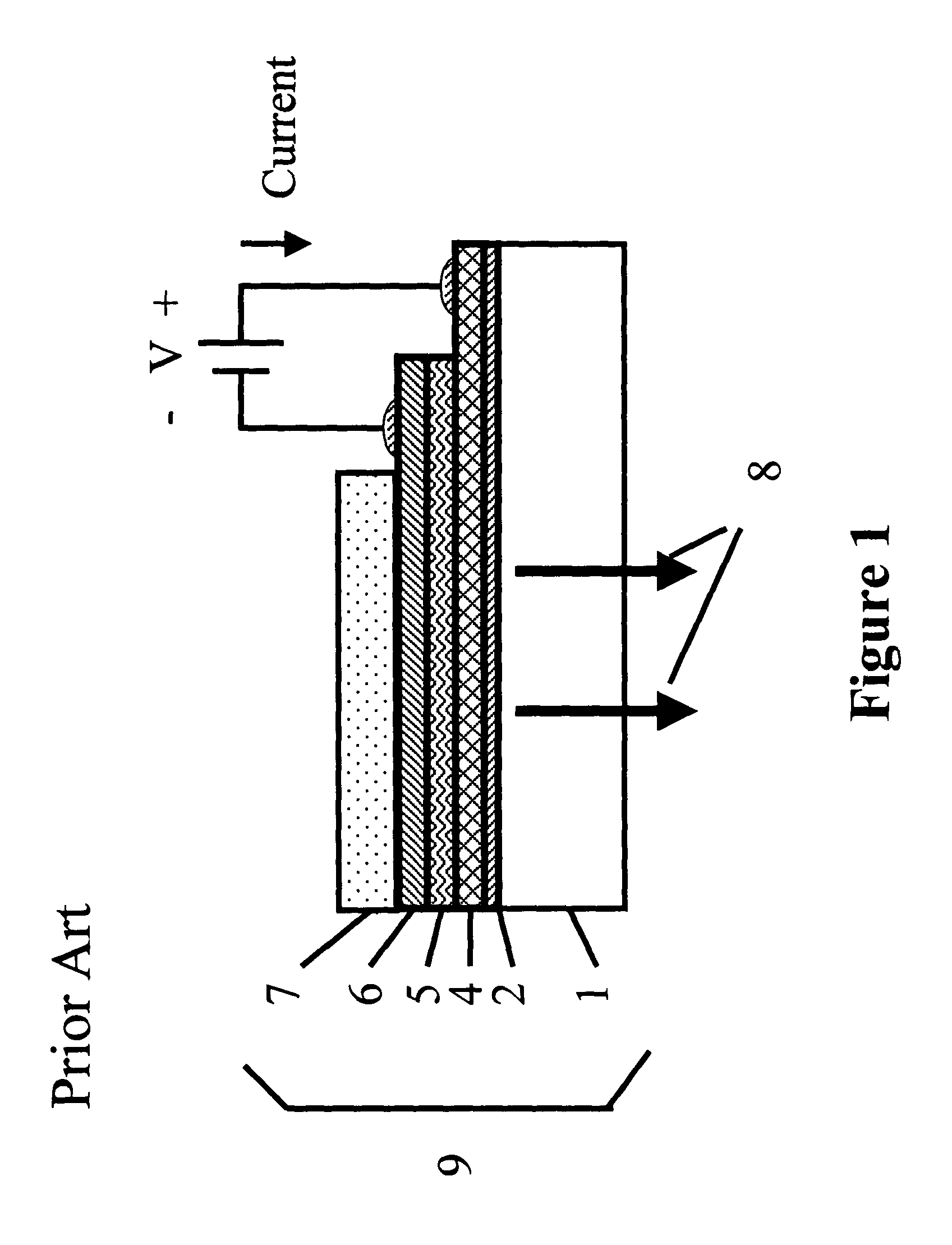
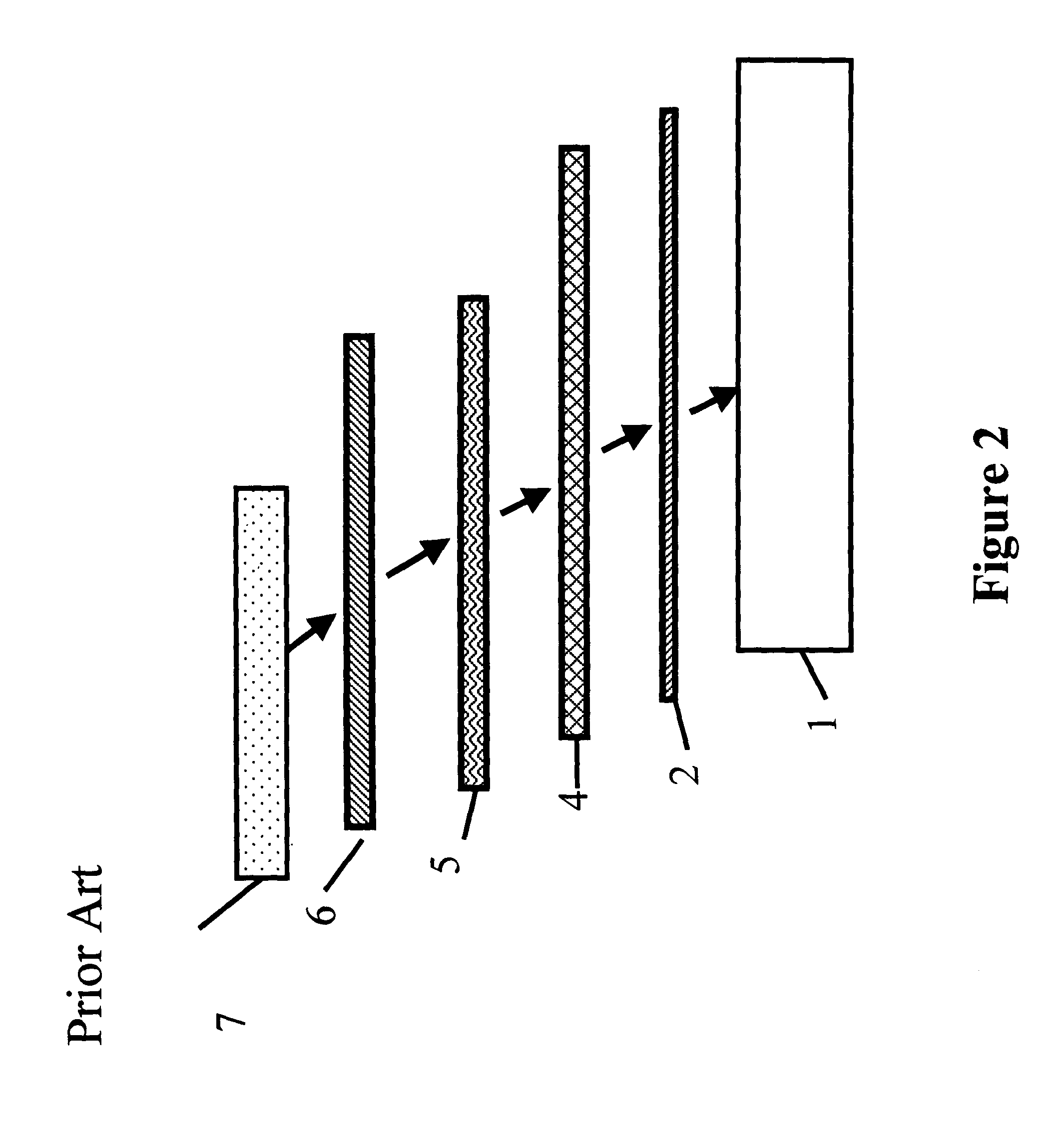
01 Materials for organic mixed ionic-electronic conductors
Various materials can be used to create organic mixed ionic-electronic conductors (MIECs), which facilitate both ionic and electronic transport. These materials include conductive polymers, organic semiconductors, and composite materials that combine organic components with inorganic elements. The selection of appropriate materials is crucial for achieving the desired balance between ionic and electronic conductivity, which affects the overall performance of devices utilizing MIECs.- Materials for mixed ionic-electronic conductors: Various organic materials can be used as mixed ionic-electronic conductors (MIECs), which facilitate both ion and electron transport simultaneously. These materials include conductive polymers, organic semiconductors, and composite materials that combine organic components with inorganic elements. The unique properties of these materials enable applications in energy storage, electrochemical devices, and sensors where efficient charge transport is critical.
- Fabrication methods for organic MIECs: Various fabrication techniques are employed to create organic mixed ionic-electronic conductors with optimized properties. These methods include solution processing, electrochemical deposition, vapor deposition, and printing technologies. The fabrication processes can be tailored to control the morphology, crystallinity, and interface properties of the materials, which directly impact their ionic and electronic transport capabilities.
- Applications in energy storage and conversion: Organic mixed ionic-electronic conductors play crucial roles in energy storage and conversion devices. They are utilized in batteries, supercapacitors, fuel cells, and solar cells where efficient charge transport is essential. The ability of these materials to conduct both ions and electrons makes them particularly valuable for improving energy density, power output, and cycling stability in these applications.
- Electrochemical transformation and doping strategies: Electrochemical methods can be used to transform and modify organic mixed ionic-electronic conductors. These include doping processes, redox reactions, and electrochemical activation that alter the electronic structure and transport properties of the materials. By controlling the electrochemical environment, the conductivity, stability, and functionality of these materials can be tuned for specific applications.
- Interface engineering and device integration: The performance of organic mixed ionic-electronic conductors in devices depends significantly on interface engineering. This involves controlling the interactions between the organic conductor and electrodes, electrolytes, or other device components. Techniques such as surface modification, composite formation, and gradient structures are employed to optimize charge transfer across interfaces, reduce contact resistance, and enhance overall device performance.
02 Applications in energy storage and conversion devices
Organic mixed ionic-electronic conductors play a significant role in energy storage and conversion devices. They are utilized in batteries, fuel cells, and supercapacitors to enhance charge transport and storage capabilities. The dual conduction mechanism allows for more efficient energy conversion processes and improved device performance. These materials can be tailored to specific applications by modifying their chemical structure and composition.Expand Specific Solutions03 Fabrication techniques for organic MIECs
Various fabrication techniques are employed to produce organic mixed ionic-electronic conductors with desired properties. These include solution processing, electrochemical deposition, vapor deposition, and printing technologies. The fabrication method significantly influences the morphology, crystallinity, and interface properties of the resulting materials, which in turn affect their conductivity and stability. Advanced processing techniques enable the creation of structured materials with enhanced performance characteristics.Expand Specific Solutions04 Transformation mechanisms in organic MIECs
The transformation mechanisms in organic mixed ionic-electronic conductors involve complex processes that affect their electrical and ionic properties. These include phase transitions, structural reorganization, doping/dedoping processes, and interfacial phenomena. Understanding these transformation mechanisms is essential for controlling the conductivity and stability of MIECs. Research focuses on elucidating the relationship between molecular structure, morphology, and the resulting transport properties to optimize material performance.Expand Specific Solutions05 Device integration and interface engineering
Successful integration of organic mixed ionic-electronic conductors into functional devices requires careful interface engineering. This involves optimizing the contact between the MIEC and electrodes, managing charge transfer across interfaces, and ensuring compatibility with other device components. Interface engineering techniques include surface modification, insertion of buffer layers, and controlled doping. These approaches help minimize contact resistance, enhance charge injection/extraction, and improve overall device stability and performance.Expand Specific Solutions
Key Industry Players in OMIEC Research and Production
The organic mixed ionic electronic conductors (OMIEC) market is currently in an early growth phase, characterized by increasing research activity and emerging commercial applications. The global market size is expanding, driven by demand for flexible electronics and sustainable semiconductor fabrication methods. Technologically, OMIECs are advancing toward maturity with key players demonstrating different levels of expertise. Samsung Electronics and Merck Patent GmbH lead in commercial applications, while Novaled GmbH specializes in OLED doping technologies. Research institutions like Nanjing University and University of Tokyo contribute fundamental innovations. BASF and Fujifilm are developing materials expertise, while Semiconductor Energy Laboratory and Idemitsu Kosan focus on integration with existing semiconductor processes. This competitive landscape reflects a technology transitioning from research to industrial implementation.
Samsung Electronics Co., Ltd.
Technical Solution: Samsung Electronics has developed an advanced OMIEC platform called "IonicTronic" that integrates organic mixed conductors into their semiconductor fabrication processes. This technology utilizes specially engineered polymers with pendant ionic groups that create nanoscale channels for controlled ion movement while maintaining electronic pathways. Samsung has successfully demonstrated transistors with tunable threshold voltages through ionic doping, achieving power reductions of approximately 40% compared to conventional CMOS technology. Their approach incorporates these materials as functional interlayers in traditional silicon-based devices, creating hybrid architectures that benefit from both technologies. Samsung has scaled this technology to 300mm wafer demonstrations, showing compatibility with existing semiconductor manufacturing infrastructure. The company has particularly focused on memory applications, where their OMIEC-based resistive switching elements have achieved switching speeds below 10ns with retention times exceeding 10 years in accelerated testing conditions, positioning these materials as potential replacements for conventional flash memory.
Strengths: Strong integration with existing semiconductor manufacturing infrastructure; demonstrated large-scale production capability; hybrid approaches that leverage both conventional and OMIEC technologies. Weaknesses: Currently limited to specific device components rather than full replacement of traditional semiconductors; higher production costs compared to fully organic approaches.
Merck Patent GmbH
Technical Solution: Merck has developed a comprehensive portfolio of OMIEC materials under their "Conductivity+" platform, specifically engineered to transform semiconductor fabrication processes. Their approach focuses on solution-processable materials that combine specially designed conjugated polymers with ionic functionalities, enabling both electronic and ionic transport within a single material system. Merck's materials achieve ionic conductivities of up to 10^-4 S/cm while maintaining electronic mobilities above 0.5 cm²/Vs, representing a balanced performance profile critical for mixed conduction applications. The company has pioneered scalable synthesis methods that maintain batch-to-batch consistency at industrial scales, addressing a key challenge in organic electronics commercialization. Their materials enable low-temperature processing (below 150°C), compatible with flexible substrates and roll-to-roll manufacturing. Merck has demonstrated particular success in electrochemical transistors where their materials show response times below 1ms and operational stability exceeding 10,000 cycles, significantly outperforming previous generations of organic mixed conductors.
Strengths: Industrial-scale production capabilities with consistent quality control; comprehensive material portfolio covering different application requirements; established supply chain integration with semiconductor manufacturers. Weaknesses: Higher material costs compared to traditional semiconductors; performance still below silicon in terms of absolute switching speed and current density.
Core Patents and Innovations in OMIEC Technology
Organic semiconductor devices and methods of fabrication including forming two parts with polymerisable groups and bonding the parts
PatentInactiveUS7063994B2
Innovation
- The approach involves constructing organic semiconductor devices by combining two parts, each formed on a substrate with specific layers, allowing for standardized fabrication in optimized environments and enabling various configurations through a combinational method that reduces equipment requirements and enhances flexibility.

Non-vacuum methods for the fabrication of organic semiconductor devices
PatentInactiveUS6949403B2
Innovation
- The development of non-vacuum electrodeposition and solution processing techniques for depositing low and high work function metals, using methods like electrodeposition and solution processing with inert atmospheres to prevent oxidation, and combining layers in inverted structures for organic semiconductor devices.


Environmental Impact and Sustainability Factors
The adoption of Organic Mixed Ionic Electronic Conductors (OMIECs) in semiconductor fabrication represents a significant shift toward more environmentally sustainable manufacturing processes. Traditional semiconductor fabrication relies heavily on energy-intensive processes and hazardous materials, contributing substantially to environmental degradation. OMIECs offer a promising alternative with reduced environmental footprint across multiple dimensions.
Energy consumption in semiconductor manufacturing facilities has historically been excessive, with conventional fabrication requiring high temperatures and vacuum conditions. OMIECs enable solution-processing techniques that operate at significantly lower temperatures and atmospheric pressure, potentially reducing energy requirements by 30-45% compared to traditional methods. This energy efficiency translates directly to reduced carbon emissions from semiconductor manufacturing operations.
Material sustainability constitutes another critical advantage of OMIEC implementation. These organic materials can be derived from renewable resources rather than the finite mineral deposits required for traditional semiconductor components. Additionally, many OMIECs demonstrate biodegradability under appropriate conditions, addressing end-of-life environmental concerns that plague conventional electronic waste management systems.
Water usage represents a particularly pressing environmental challenge in semiconductor fabrication, with traditional processes consuming millions of gallons daily. OMIEC-based manufacturing techniques typically require substantially less water, with some solution processes demonstrating up to 70% reduction in water consumption. This benefit becomes increasingly valuable as water scarcity affects more regions globally.
Chemical waste reduction stands as perhaps the most significant environmental advantage of OMIEC technology. Conventional semiconductor fabrication utilizes numerous toxic chemicals including heavy metals, strong acids, and specialized gases with high global warming potential. OMIEC processes typically employ more benign solvents and eliminate many hazardous materials entirely, reducing both environmental contamination risk and worker exposure to dangerous substances.
Life cycle assessment studies indicate that OMIEC-based semiconductor components generally demonstrate superior environmental performance across multiple impact categories, including resource depletion, ecotoxicity, and climate change potential. However, challenges remain in scaling these benefits to industrial production levels while maintaining the performance characteristics required for advanced applications.
Regulatory frameworks increasingly favor technologies with improved environmental profiles, positioning OMIEC-based semiconductor fabrication advantageously as environmental compliance requirements intensify globally. Companies adopting these technologies may benefit from reduced compliance costs and improved corporate sustainability metrics, creating additional market incentives beyond the direct environmental benefits.
Cost-Benefit Analysis of OMIEC Integration
The integration of Organic Mixed Ionic Electronic Conductors (OMIECs) into semiconductor fabrication processes presents a complex economic equation that industry stakeholders must carefully evaluate. Initial implementation costs are substantial, requiring significant capital investment in specialized equipment, facility modifications, and staff training. Companies adopting OMIEC technology face upfront expenditures ranging from $10-50 million depending on production scale, with additional R&D costs for process optimization that may extend the return-on-investment timeline to 3-5 years.
Material costs represent another critical consideration. While traditional semiconductor materials have established supply chains and predictable pricing, OMIECs currently command premium prices due to limited production volume and specialized synthesis requirements. However, analysis indicates that as adoption increases, economies of scale could reduce OMIEC material costs by 30-45% within the next decade, potentially reaching price parity with conventional alternatives for certain applications.
Energy efficiency emerges as a major benefit in the OMIEC value proposition. Fabrication processes utilizing these materials typically consume 20-35% less energy than traditional methods, primarily due to lower temperature requirements and reduced process steps. This translates to operational savings of approximately $1.2-2.5 million annually for medium-scale production facilities, with additional environmental benefits through reduced carbon emissions.
Product performance advantages deliver compelling long-term value. Devices incorporating OMIECs demonstrate 15-40% improvements in energy efficiency, significantly extended operational lifespans, and enhanced functionality in flexible/wearable applications. These performance gains enable premium pricing strategies and expanded market opportunities that can generate 25-60% higher profit margins compared to conventional semiconductor products.
Manufacturing flexibility represents another significant benefit. OMIEC-based processes can reduce production line changeover times by up to 70% and enable smaller batch production without prohibitive cost penalties. This agility allows manufacturers to respond more rapidly to market demands and reduce inventory carrying costs, creating operational savings estimated at 8-15% of total production expenses.
Regulatory considerations must also factor into cost-benefit calculations. While OMIECs generally align with sustainability initiatives and may qualify for environmental incentives in certain regions, companies must navigate evolving regulatory frameworks regarding novel materials. Compliance costs vary significantly by jurisdiction but typically add 3-7% to implementation expenses during early adoption phases.
Unlock deeper insights with PatSnap Eureka Quick Research — get a full tech report to explore trends and direct your research. Try now!
Generate Your Research Report Instantly with AI Agent
Supercharge your innovation with PatSnap Eureka AI Agent Platform!