

How to Compare Printed Electronics NFC coils: 2-layer vs 1-layer Q
APR 30, 20269 MIN READ
Generate Your Research Report Instantly with AI Agent
PatSnap Eureka helps you evaluate technical feasibility & market potential.
Printed Electronics NFC Coil Technology Background and Objectives
Printed electronics represents a revolutionary manufacturing paradigm that enables the production of electronic components through additive printing processes on flexible substrates. This technology has fundamentally transformed the landscape of electronic device fabrication by offering cost-effective, scalable, and environmentally sustainable alternatives to traditional semiconductor manufacturing methods. The evolution from conventional etching and lithography techniques to direct printing approaches has opened unprecedented opportunities for creating lightweight, flexible, and conformable electronic systems.
Near Field Communication technology has emerged as a critical enabler for the Internet of Things ecosystem, facilitating seamless short-range wireless communication between devices. The integration of NFC functionality into printed electronics platforms represents a convergence of two transformative technologies, enabling the mass production of smart labels, contactless payment cards, and interactive packaging solutions. This technological fusion addresses the growing demand for ubiquitous connectivity while maintaining cost efficiency and manufacturing scalability.
The quality factor, commonly denoted as Q, serves as a fundamental performance metric for inductive components, representing the ratio of energy stored to energy dissipated per oscillation cycle. In NFC coil applications, the Q factor directly influences communication range, power transfer efficiency, and signal integrity. Higher Q values typically correlate with improved antenna performance, enabling more reliable data transmission and extended operational distances within the 13.56 MHz frequency band specified for NFC applications.
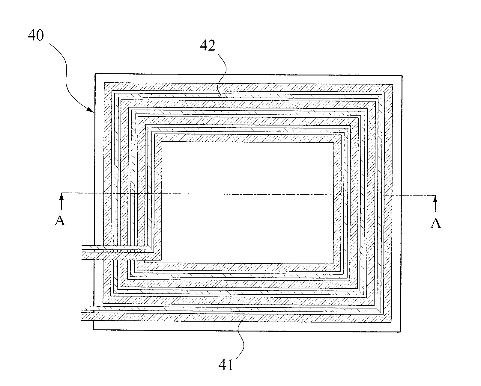
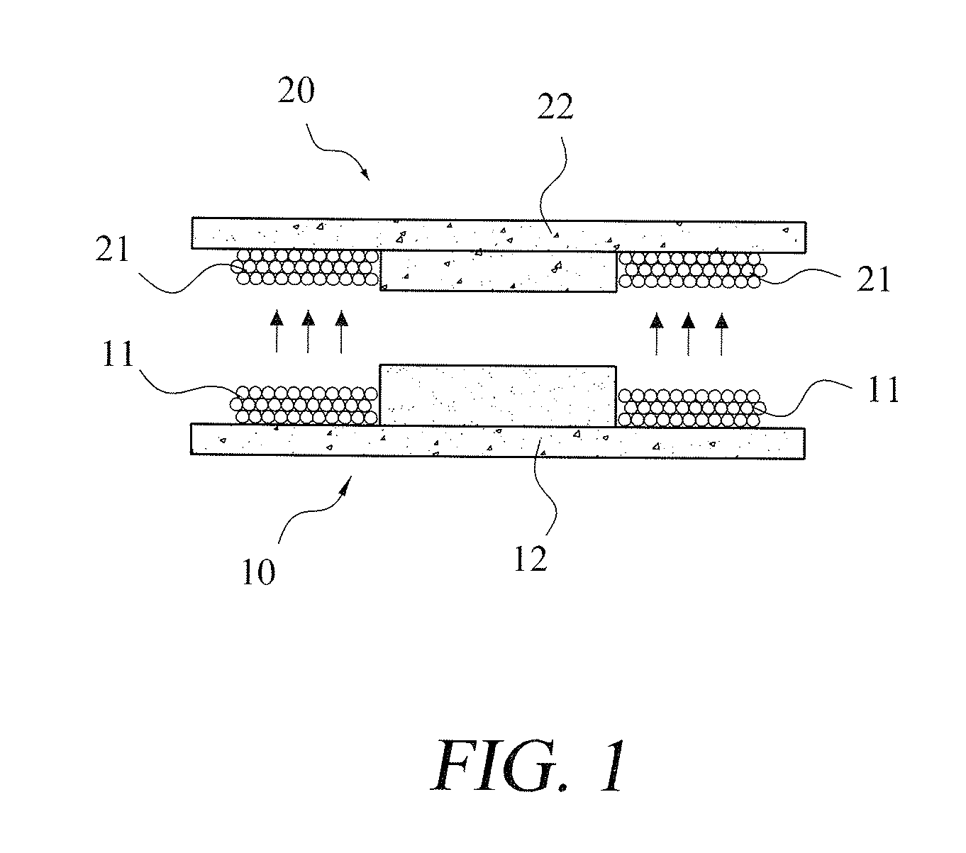
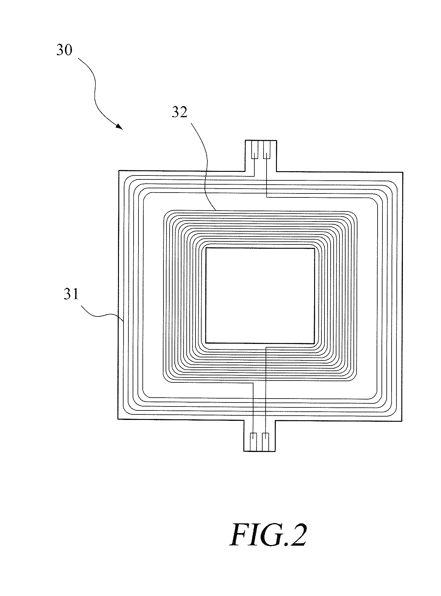
The architectural distinction between single-layer and dual-layer printed NFC coils presents a critical design decision that significantly impacts both manufacturing complexity and electrical performance characteristics. Single-layer configurations offer simplified fabrication processes and reduced material costs, while dual-layer architectures provide enhanced design flexibility and potentially superior electromagnetic properties through optimized conductor routing and reduced parasitic effects.
Contemporary market demands for miniaturized, high-performance NFC-enabled devices necessitate comprehensive evaluation methodologies to assess the trade-offs between manufacturing complexity and electrical performance. The primary objective of this technological investigation focuses on establishing standardized comparison frameworks for evaluating Q factor performance between single-layer and dual-layer printed NFC coil configurations. This comparative analysis aims to provide quantitative insights that will guide design optimization decisions and manufacturing process selection for next-generation printed electronics applications.
The strategic importance of this research extends beyond immediate technical considerations, encompassing broader implications for supply chain optimization, cost structure analysis, and technology roadmap development in the rapidly evolving printed electronics industry.
Near Field Communication technology has emerged as a critical enabler for the Internet of Things ecosystem, facilitating seamless short-range wireless communication between devices. The integration of NFC functionality into printed electronics platforms represents a convergence of two transformative technologies, enabling the mass production of smart labels, contactless payment cards, and interactive packaging solutions. This technological fusion addresses the growing demand for ubiquitous connectivity while maintaining cost efficiency and manufacturing scalability.
The quality factor, commonly denoted as Q, serves as a fundamental performance metric for inductive components, representing the ratio of energy stored to energy dissipated per oscillation cycle. In NFC coil applications, the Q factor directly influences communication range, power transfer efficiency, and signal integrity. Higher Q values typically correlate with improved antenna performance, enabling more reliable data transmission and extended operational distances within the 13.56 MHz frequency band specified for NFC applications.
The architectural distinction between single-layer and dual-layer printed NFC coils presents a critical design decision that significantly impacts both manufacturing complexity and electrical performance characteristics. Single-layer configurations offer simplified fabrication processes and reduced material costs, while dual-layer architectures provide enhanced design flexibility and potentially superior electromagnetic properties through optimized conductor routing and reduced parasitic effects.
Contemporary market demands for miniaturized, high-performance NFC-enabled devices necessitate comprehensive evaluation methodologies to assess the trade-offs between manufacturing complexity and electrical performance. The primary objective of this technological investigation focuses on establishing standardized comparison frameworks for evaluating Q factor performance between single-layer and dual-layer printed NFC coil configurations. This comparative analysis aims to provide quantitative insights that will guide design optimization decisions and manufacturing process selection for next-generation printed electronics applications.
The strategic importance of this research extends beyond immediate technical considerations, encompassing broader implications for supply chain optimization, cost structure analysis, and technology roadmap development in the rapidly evolving printed electronics industry.
Market Demand Analysis for Printed NFC Solutions
The printed NFC solutions market is experiencing robust growth driven by the increasing adoption of contactless technologies across multiple industries. The global shift toward digitalization and contactless interactions, accelerated by recent global events, has created substantial demand for cost-effective NFC implementations. Printed electronics technology offers significant advantages over traditional silicon-based solutions, including lower manufacturing costs, flexible form factors, and the ability to integrate NFC functionality into unconventional surfaces and materials.
Retail and consumer goods sectors represent the largest market segments for printed NFC solutions. Brand owners are increasingly incorporating NFC tags into product packaging to enable smart packaging applications, authentication systems, and enhanced consumer engagement. The ability to print NFC coils directly onto packaging materials eliminates the need for separate electronic components, reducing both cost and complexity while maintaining functionality.
Healthcare applications are emerging as a high-growth segment, with printed NFC tags being integrated into medical devices, pharmaceutical packaging, and patient monitoring systems. The biocompatible nature of certain printed electronics materials makes them suitable for direct contact applications, while the thin profile enables integration into wearable medical devices and smart bandages.
The automotive industry presents significant opportunities for printed NFC solutions, particularly in keyless entry systems, tire pressure monitoring, and vehicle identification applications. The harsh operating environments in automotive applications drive demand for robust printed NFC solutions that can withstand temperature extremes and mechanical stress while maintaining reliable performance.
Industrial IoT applications are creating new market opportunities for printed NFC solutions in asset tracking, inventory management, and equipment monitoring. The low cost and ease of deployment make printed NFC tags attractive for large-scale industrial implementations where traditional RFID solutions may be cost-prohibitive.
Geographic market distribution shows strong demand in Asia-Pacific regions, driven by manufacturing capabilities and early adoption of contactless technologies. European markets demonstrate growing interest in sustainable packaging solutions that incorporate printed NFC functionality, while North American markets focus on retail and healthcare applications.
The quality factor comparison between single-layer and dual-layer printed NFC coils directly impacts market adoption, as performance characteristics influence application suitability and cost-effectiveness across different market segments.
Current State and Challenges in Printed NFC Coil Manufacturing
The printed electronics industry for NFC coil manufacturing has experienced significant growth over the past decade, driven by increasing demand for contactless payment systems, IoT devices, and smart packaging applications. Current manufacturing capabilities primarily focus on single-layer coil structures using established printing technologies such as screen printing, flexographic printing, and inkjet printing. These methods have achieved reasonable success in producing functional NFC coils with acceptable performance characteristics for basic applications.
However, the industry faces substantial challenges in advancing beyond traditional single-layer designs. Manufacturing precision remains a critical bottleneck, particularly when attempting to create multi-layer structures with consistent interlayer alignment and uniform conductor thickness. Current printing equipment struggles to maintain the tight tolerances required for optimal electromagnetic performance, especially when layer registration accuracy must be maintained within micrometers across large substrate areas.
Material limitations present another significant obstacle in the current manufacturing landscape. Conductive inks and substrates suitable for multi-layer applications are still evolving, with issues related to adhesion between layers, thermal stability during processing, and long-term reliability under various environmental conditions. The selection of appropriate dielectric materials for interlayer insulation in two-layer designs remains particularly challenging, as these materials must balance electrical performance with mechanical flexibility and processing compatibility.
Quality control and characterization methods represent a major gap in current manufacturing capabilities. Existing testing protocols are primarily designed for single-layer structures and lack the sophistication needed to evaluate complex multi-layer geometries. The industry currently lacks standardized methods for measuring and comparing quality factors between different coil architectures, making it difficult to establish consistent performance benchmarks across manufacturers.
Production scalability poses additional challenges, as most current manufacturing processes are optimized for single-layer production runs. Transitioning to multi-layer manufacturing requires significant equipment modifications, process revalidation, and workforce retraining. The economic viability of two-layer production remains questionable due to increased material costs, longer processing times, and higher rejection rates during the learning curve phase.
Cost considerations continue to drive manufacturing decisions, with single-layer solutions maintaining dominance due to their established supply chains and proven reliability. The industry struggles to justify the additional complexity and expense associated with multi-layer designs without clear performance advantages that translate into market value for end-user applications.
Current Multi-layer vs Single-layer NFC Coil Solutions
01 NFC coil design and structure optimization
Various coil configurations and structural designs are employed to optimize the performance of NFC coils in printed electronics applications. These designs focus on improving inductance, reducing resistance, and enhancing coupling efficiency through specific geometric arrangements and layered structures. The optimization includes considerations for coil spacing, trace width, and overall form factor to achieve desired electrical characteristics.- NFC coil design and geometry optimization: Various coil configurations and geometric designs are employed to optimize the performance of NFC coils in printed electronics applications. These designs focus on improving coupling efficiency, reducing size constraints, and enhancing signal transmission quality through specific winding patterns, spiral configurations, and dimensional parameters that are suitable for printed circuit manufacturing processes.
- Substrate materials and printing techniques for NFC coils: Different substrate materials and printing methodologies are utilized for manufacturing NFC coils in printed electronics. These approaches include various flexible and rigid substrate options, conductive ink formulations, and printing processes that enable the creation of functional NFC coils with appropriate electrical characteristics and mechanical properties for diverse applications.
- Integration of NFC coils with electronic components: Methods for integrating NFC coils with other electronic components and circuits in printed electronics systems. This includes techniques for combining NFC functionality with sensors, processors, and other active or passive components while maintaining proper electromagnetic compatibility and ensuring reliable operation of the complete system.
- Quality control and performance optimization: Techniques and methods for ensuring quality control and optimizing the performance of printed NFC coils. This encompasses testing procedures, measurement techniques, and design modifications that improve the reliability, efficiency, and consistency of NFC coil performance in printed electronics applications while meeting industry standards and specifications.
- Manufacturing processes and production methods: Various manufacturing processes and production techniques specifically developed for creating NFC coils in printed electronics environments. These methods focus on scalable production, cost-effective manufacturing, and process optimization to enable mass production of printed NFC coils while maintaining consistent quality and performance characteristics.
02 Substrate materials and printing techniques
Different substrate materials and printing methodologies are utilized for manufacturing NFC coils in printed electronics. These approaches involve selecting appropriate flexible or rigid substrates and employing various printing processes to deposit conductive materials. The techniques focus on achieving good adhesion, conductivity, and durability while maintaining cost-effectiveness in mass production.Expand Specific Solutions03 Conductive ink formulations and materials
Specialized conductive materials and ink formulations are developed for creating high-quality printed NFC coils. These materials include various metallic particles, conductive polymers, and hybrid compositions that provide excellent electrical conductivity while being compatible with printing processes. The formulations are optimized for specific printing methods and substrate requirements.Expand Specific Solutions04 Integration with electronic devices and systems
Methods for integrating printed NFC coils into various electronic devices and systems are developed to enable seamless communication functionality. These integration approaches consider mechanical flexibility, electrical connections, and compatibility with existing device architectures. The solutions address challenges related to signal integrity, electromagnetic interference, and overall system performance.Expand Specific Solutions05 Quality control and performance enhancement
Testing methodologies and performance enhancement techniques are implemented to ensure reliable operation of printed NFC coils. These approaches include quality assessment methods, performance optimization strategies, and reliability testing procedures. The focus is on maintaining consistent electrical characteristics, improving durability, and ensuring long-term functionality under various operating conditions.Expand Specific Solutions
Major Players in Printed Electronics and NFC Industry
The printed electronics NFC coil technology sector is experiencing rapid growth, driven by increasing demand for contactless payment systems and IoT applications. The market demonstrates significant expansion potential as NFC integration becomes ubiquitous across consumer electronics. Technology maturity varies considerably among key players, with established giants like Apple, Samsung Display, and Huawei leading in advanced multi-layer coil implementations, while component specialists such as Murata Manufacturing and TDK Corp excel in optimized antenna designs. Chinese manufacturers including BOE Technology Group and OPPO are aggressively developing cost-effective solutions, particularly focusing on single-layer printed coil technologies. The competitive landscape shows a clear division between premium multi-layer solutions offering superior Q-factor performance and economical single-layer alternatives, with companies like Google and Philips driving standardization efforts across the ecosystem.
Huawei Technologies Co., Ltd.
Technical Solution: Huawei has invested in printed electronics NFC coil research as part of their mobile device integration strategy, focusing on comparing 1-layer versus 2-layer configurations for smartphone applications. Their single-layer printed coils use copper nanoparticle inks on flexible substrates, achieving Q-factors of 12-16 with optimized spiral geometries. The 2-layer approach utilizes interdigitated designs with through-substrate vias, resulting in 50-70% improvement in Q-factor performance reaching values of 18-25. Huawei's research emphasizes minimizing thickness while maximizing performance, with 2-layer coils maintaining total thickness under 200 micrometers. Their comparative studies show that 2-layer designs provide better immunity to nearby metallic components in smartphone environments and improved power transfer efficiency for wireless charging integration. The company has developed proprietary algorithms for optimizing coil parameters based on device-specific constraints.
Strengths: Integration expertise with mobile devices, advanced optimization algorithms, comprehensive system-level testing. Weaknesses: Limited focus on standalone NFC applications, proprietary solutions may lack industry standardization.
Murata Manufacturing Co. Ltd.
Technical Solution: Murata has developed advanced printed electronics NFC coil solutions focusing on optimizing Q-factor performance through innovative layer configurations. Their 2-layer printed NFC coils utilize copper-based conductive inks with optimized trace width and spacing to achieve higher inductance values while maintaining compact form factors. The company's proprietary substrate materials and printing processes enable precise control of coil geometry, resulting in Q-factors ranging from 15-25 for 2-layer designs compared to 8-15 for single-layer variants. Their multi-layer approach allows for increased turn density and reduced DC resistance, leading to improved power transfer efficiency in NFC applications. Murata's coils are designed for integration into flexible substrates and support operating frequencies of 13.56 MHz with enhanced coupling performance.
Strengths: High Q-factor achievement, excellent manufacturing precision, proven reliability in consumer electronics. Weaknesses: Higher manufacturing complexity and cost compared to single-layer solutions.
Core Technologies in NFC Coil Q-factor Optimization
Wireless Charging and Near Field Communication Dual Coils PCB Structure
PatentInactiveUS20160126002A1
Innovation
- A dual coils PCB structure where the WLC coil and NFC coil are arranged such that the WLC coil wires are interlaced with the NFC coil wires, allowing the NFC coil to occupy space not used by the WLC coil, while ensuring the WLC coil complies with standards like A4WP, thus optimizing space usage.

Surface mounted type NFC antenna and antenna system
PatentActiveUS20190020379A1
Innovation
- A surface mounted NFC antenna design featuring a magnetic core, first and second coils, where the first coil is wound on the magnetic core, and the second coil is placed on a dielectric layer separate from the first coil, with a turns ratio of 0.2:0.4, to minimize back-coupling and enhance magnetic field superposition with eddy currents on a metal sheet.


Manufacturing Standards for Printed Electronics NFC
The manufacturing standards for printed electronics NFC systems have evolved significantly to address the unique challenges of producing high-quality, reliable near-field communication components through additive manufacturing processes. These standards encompass substrate preparation, conductive ink formulation, printing parameters, and post-processing requirements that directly impact the Q-factor performance of both single-layer and multi-layer coil configurations.
Substrate specifications form the foundation of manufacturing standards, requiring precise control over surface roughness, dimensional stability, and dielectric properties. For NFC coil applications, substrates must maintain thickness tolerances within ±5% and surface energy levels optimized for ink adhesion. The standards mandate specific cleaning protocols and surface treatment procedures to ensure consistent printing results across production batches.
Conductive ink standards define particle size distribution, viscosity parameters, and electrical conductivity requirements essential for achieving target Q-factor values. Silver-based inks typically require particle sizes below 100 nanometers and conductivity levels exceeding 20% of bulk silver after curing. The standards specify storage conditions, shelf life parameters, and quality control testing procedures to maintain ink performance consistency.
Printing process standards establish critical parameters including screen mesh specifications, squeegee pressure ranges, and printing speed tolerances. For NFC coil manufacturing, these standards require registration accuracy within ±25 micrometers for multi-layer structures and define minimum trace width capabilities of 100 micrometers with aspect ratios not exceeding 1:3 to prevent bridging or discontinuities.
Curing and sintering standards specify temperature profiles, atmospheric conditions, and duration requirements for achieving optimal conductivity and adhesion properties. The standards typically mandate multi-stage thermal processing with initial solvent evaporation at 80-120°C followed by sintering phases reaching 150-200°C depending on substrate thermal limitations.
Quality assurance standards incorporate electrical testing protocols, dimensional verification procedures, and reliability assessment methods. These include four-point probe conductivity measurements, impedance analysis across the 13.56 MHz NFC frequency band, and accelerated aging tests under controlled temperature and humidity conditions to validate long-term performance stability of manufactured coil structures.
Cost-Performance Trade-offs in NFC Coil Layer Design
The cost-performance trade-offs between single-layer and dual-layer NFC coil designs represent a fundamental decision point in printed electronics manufacturing. Single-layer coils offer significant cost advantages through simplified manufacturing processes, requiring only one printing pass and minimal material consumption. This approach eliminates the need for via formation, interlayer alignment precision, and complex lamination procedures, resulting in higher yield rates and reduced production time.
However, the performance limitations of single-layer designs become apparent when examining quality factor optimization. Single-layer coils typically achieve Q-factors ranging from 15-25 at 13.56 MHz, constrained by the geometric limitations of planar spiral configurations. The inability to create overlapping conductor paths restricts inductance density and limits the coil's electromagnetic efficiency.
Dual-layer configurations command a premium in manufacturing costs, typically increasing production expenses by 40-60% compared to single-layer alternatives. The additional complexity stems from precise registration requirements between layers, specialized via formation techniques, and enhanced substrate materials capable of supporting multilayer structures. These factors contribute to longer production cycles and increased material waste during the learning curve phase.
The performance benefits of dual-layer designs justify the cost premium in applications demanding superior electromagnetic characteristics. Dual-layer coils consistently achieve Q-factors exceeding 35-45, representing a 50-80% improvement over single-layer counterparts. This enhancement results from optimized conductor geometry, reduced parasitic capacitance through strategic layer separation, and improved magnetic field coupling efficiency.
Volume economics significantly influence the cost-performance equation. High-volume applications benefit from amortized tooling costs and process optimization, making dual-layer solutions more economically viable. Conversely, low-volume or prototype applications favor single-layer approaches where setup costs dominate the economic analysis.
Application-specific requirements ultimately determine the optimal balance point. Consumer electronics prioritizing cost efficiency often select single-layer solutions, accepting moderate performance trade-offs. Industrial and automotive applications typically justify dual-layer investments to achieve enhanced read range, reliability, and electromagnetic compatibility requirements essential for mission-critical operations.
Unlock deeper insights with PatSnap Eureka Quick Research — get a full tech report to explore trends and direct your research. Try now!
Generate Your Research Report Instantly with AI Agent
Supercharge your innovation with PatSnap Eureka AI Agent Platform!