

How to Compare Printed Electronics Stretchability: wavy vs straight traces
APR 30, 20269 MIN READ
Generate Your Research Report Instantly with AI Agent
PatSnap Eureka helps you evaluate technical feasibility & market potential.
Printed Electronics Stretchability Background and Objectives
Printed electronics represents a revolutionary manufacturing paradigm that enables the deposition of electronic materials onto flexible substrates through various printing techniques including inkjet printing, screen printing, and gravure printing. This technology has emerged as a critical enabler for next-generation flexible and wearable electronic devices, offering unprecedented opportunities for creating conformable circuits that can adapt to complex three-dimensional surfaces and withstand mechanical deformation during operation.
The fundamental challenge in printed electronics lies in maintaining electrical functionality while accommodating mechanical stress and strain. Traditional rigid electronic circuits fail catastrophically when subjected to bending, stretching, or twisting forces. However, printed electronic systems must operate reliably under these conditions to fulfill their promise in applications ranging from flexible displays and electronic skin to smart textiles and biomedical implants.
Stretchability has become a paramount design consideration as it directly impacts device reliability, operational lifespan, and application scope. The ability of printed conductive traces to maintain electrical continuity under mechanical deformation determines the overall system performance and durability. This mechanical robustness is particularly crucial for wearable devices that experience continuous flexing and stretching during normal use.
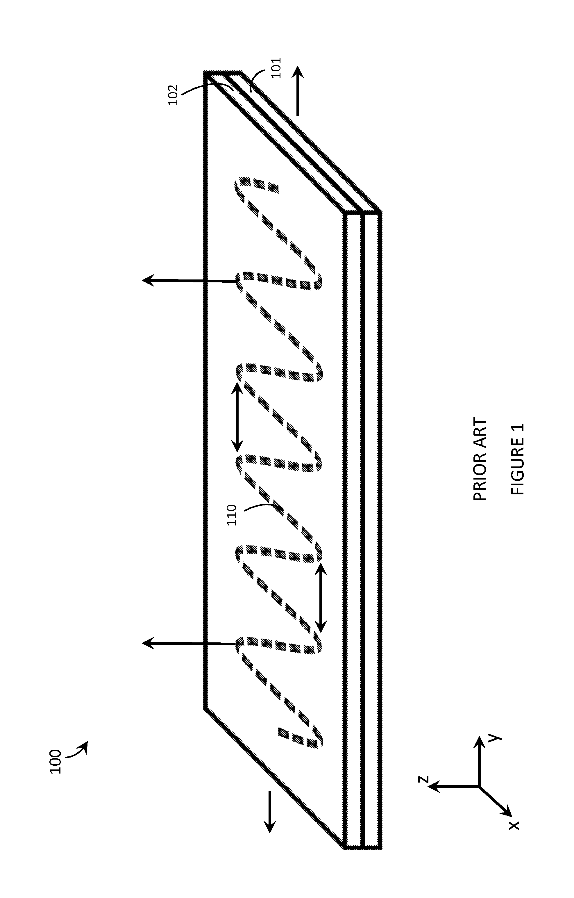
Two primary trace design approaches have emerged to address stretchability requirements: wavy trace geometries and straight trace configurations. Wavy traces incorporate serpentine or sinusoidal patterns that theoretically provide mechanical compliance through geometric accommodation of strain. Straight traces rely on material properties and substrate interactions to maintain functionality under deformation. Each approach presents distinct advantages and limitations in terms of electrical performance, manufacturing complexity, and mechanical reliability.
The comparative evaluation of these trace designs requires comprehensive understanding of electromechanical behavior, failure mechanisms, and performance metrics. Current research efforts focus on developing standardized testing methodologies and establishing quantitative frameworks for comparing stretchability performance across different design paradigms.
The primary objective of this technical investigation is to establish a systematic methodology for comparing the stretchability performance of wavy versus straight printed electronic traces. This includes developing standardized testing protocols, identifying key performance indicators, and creating predictive models that can guide design optimization. The research aims to provide actionable insights for engineers and designers working on flexible electronic systems, ultimately advancing the field toward more reliable and robust printed electronic devices.
The fundamental challenge in printed electronics lies in maintaining electrical functionality while accommodating mechanical stress and strain. Traditional rigid electronic circuits fail catastrophically when subjected to bending, stretching, or twisting forces. However, printed electronic systems must operate reliably under these conditions to fulfill their promise in applications ranging from flexible displays and electronic skin to smart textiles and biomedical implants.
Stretchability has become a paramount design consideration as it directly impacts device reliability, operational lifespan, and application scope. The ability of printed conductive traces to maintain electrical continuity under mechanical deformation determines the overall system performance and durability. This mechanical robustness is particularly crucial for wearable devices that experience continuous flexing and stretching during normal use.
Two primary trace design approaches have emerged to address stretchability requirements: wavy trace geometries and straight trace configurations. Wavy traces incorporate serpentine or sinusoidal patterns that theoretically provide mechanical compliance through geometric accommodation of strain. Straight traces rely on material properties and substrate interactions to maintain functionality under deformation. Each approach presents distinct advantages and limitations in terms of electrical performance, manufacturing complexity, and mechanical reliability.
The comparative evaluation of these trace designs requires comprehensive understanding of electromechanical behavior, failure mechanisms, and performance metrics. Current research efforts focus on developing standardized testing methodologies and establishing quantitative frameworks for comparing stretchability performance across different design paradigms.
The primary objective of this technical investigation is to establish a systematic methodology for comparing the stretchability performance of wavy versus straight printed electronic traces. This includes developing standardized testing protocols, identifying key performance indicators, and creating predictive models that can guide design optimization. The research aims to provide actionable insights for engineers and designers working on flexible electronic systems, ultimately advancing the field toward more reliable and robust printed electronic devices.
Market Demand for Flexible Printed Electronics Applications
The flexible printed electronics market is experiencing unprecedented growth driven by the convergence of consumer demand for bendable devices and industrial requirements for conformable electronic systems. Wearable technology represents the largest application segment, encompassing fitness trackers, smartwatches, and health monitoring patches that require circuits capable of withstanding repeated mechanical deformation during daily use. The stretchability characteristics of printed traces directly impact product reliability and user experience in these applications.
Healthcare applications constitute another rapidly expanding market segment, particularly for biomedical sensors and electronic skin patches that must conform to curved body surfaces while maintaining electrical functionality. These applications demand printed electronics with superior stretchability to accommodate skin movement, breathing, and other physiological motions without circuit failure. The comparison between wavy and straight trace designs becomes critical for ensuring long-term device performance in medical environments.
Consumer electronics manufacturers are increasingly integrating flexible printed circuits into smartphones, tablets, and foldable displays. The automotive industry represents an emerging high-value market segment, where flexible electronics enable curved dashboard displays, seat-integrated heating elements, and conformable sensor arrays. These applications require printed traces that can withstand thermal cycling, vibration, and mechanical stress while maintaining electrical integrity over extended operational periods.
The Internet of Things ecosystem is driving demand for flexible sensors that can be integrated into irregular surfaces, packaging materials, and structural components. Smart packaging applications require printed electronics capable of conforming to various container shapes while providing sensing and communication capabilities. Industrial monitoring systems increasingly rely on flexible sensor networks that must adapt to curved pipes, rotating machinery, and other non-planar surfaces.
Market growth is further accelerated by advancements in printing technologies and conductive materials that enable cost-effective production of stretchable circuits. The ability to optimize trace geometry for specific stretchability requirements directly influences manufacturing yields and product performance, making the wavy versus straight trace comparison essential for market competitiveness and application success across diverse industry sectors.
Current Challenges in Printed Electronics Mechanical Flexibility
The mechanical flexibility of printed electronics faces fundamental challenges rooted in the inherent mismatch between rigid electronic materials and flexible substrates. Traditional conductive materials such as silver nanoparticles, copper, and carbon-based inks exhibit excellent electrical properties but demonstrate limited mechanical compliance when subjected to stretching, bending, or twisting forces. This material incompatibility creates stress concentrations that lead to crack formation, delamination, and ultimately circuit failure under mechanical deformation.
Substrate-conductor interface adhesion represents another critical challenge affecting the long-term reliability of flexible printed electronics. Poor interfacial bonding between conductive traces and polymer substrates results in premature failure modes, particularly under cyclic loading conditions. The thermal expansion coefficient mismatch between metallic conductors and organic substrates exacerbates this issue, creating additional stress during temperature variations commonly encountered in real-world applications.
Manufacturing process limitations significantly impact the achievable mechanical flexibility of printed electronic devices. Current printing techniques, including screen printing, inkjet printing, and gravure printing, often require high-temperature curing processes that can induce residual stresses within the printed structures. These manufacturing-induced stresses reduce the overall mechanical robustness and create preferential failure sites during subsequent mechanical loading.
The geometric design of conductive traces presents a complex optimization challenge between electrical performance and mechanical flexibility. Straight trace geometries offer superior electrical conductivity and minimal resistance but demonstrate poor stretchability due to their inability to accommodate mechanical deformation without direct material strain. Conversely, wavy or serpentine trace designs provide enhanced mechanical compliance through geometric accommodation of strain but introduce increased electrical resistance and potential signal integrity issues.
Standardization of mechanical testing protocols remains a significant challenge in the field. The absence of universally accepted testing methodologies makes it difficult to compare stretchability performance across different trace geometries, materials, and manufacturing processes. Current testing approaches vary widely in terms of strain rates, environmental conditions, and failure criteria, leading to inconsistent and incomparable results across research studies and industrial applications.
Environmental stability under mechanical stress poses additional challenges for printed electronics deployment. Factors such as humidity, temperature cycling, and chemical exposure can significantly alter the mechanical properties of both substrates and conductive materials, leading to unpredictable performance degradation over time. The interaction between environmental factors and mechanical stress creates complex failure mechanisms that are difficult to predict and mitigate through current design approaches.
Existing Trace Design Solutions for Enhanced Stretchability
01 Stretchable substrate materials and flexible electronics
Development of stretchable substrate materials that can accommodate mechanical deformation while maintaining electronic functionality. These materials enable the creation of flexible electronic devices that can bend, stretch, and conform to various surfaces without losing their electrical properties. The substrates are designed to handle stress and strain while preserving the integrity of printed electronic components.- Stretchable substrate materials and flexible electronics: Development of stretchable substrate materials that can accommodate mechanical deformation while maintaining electronic functionality. These materials enable the creation of flexible electronic devices that can bend, stretch, and conform to various surfaces without losing their electrical properties. The substrates are designed to handle stress and strain while preserving the integrity of printed electronic components.
- Conductive inks and materials for stretchable applications: Formulation of specialized conductive inks and materials that maintain electrical conductivity under mechanical stress and deformation. These materials are engineered to provide stable electrical performance when subjected to stretching, bending, or twisting forces. The conductive materials are optimized for printing processes while ensuring durability and reliability in flexible electronic applications.
- Manufacturing processes for stretchable printed electronics: Advanced manufacturing techniques and processes specifically designed for producing stretchable printed electronic devices. These methods include specialized printing technologies, curing processes, and fabrication techniques that ensure proper adhesion and functionality of electronic components on flexible substrates. The processes are optimized to create reliable connections and maintain performance under mechanical stress.
- Interconnect structures and circuit design for flexibility: Design and implementation of interconnect structures and circuit layouts that can withstand mechanical deformation without failure. These designs incorporate serpentine patterns, mesh structures, and other geometric configurations that distribute stress and maintain electrical continuity during stretching or bending. The interconnect architectures are specifically engineered to accommodate the mechanical requirements of flexible applications.
- Encapsulation and protection methods for stretchable devices: Development of protective encapsulation techniques and barrier materials that preserve the functionality of stretchable printed electronics while maintaining flexibility. These methods provide protection against environmental factors such as moisture, oxygen, and mechanical wear while allowing the device to maintain its stretchable properties. The encapsulation solutions are designed to move with the device without compromising protection or performance.
02 Conductive inks and materials for stretchable applications
Formulation of specialized conductive inks and materials that maintain electrical conductivity under mechanical stress and deformation. These materials are engineered to provide stable electrical performance even when subjected to stretching, bending, or twisting forces. The conductive materials are optimized for printability while ensuring durability and reliability in flexible electronic applications.Expand Specific Solutions03 Manufacturing processes for stretchable printed electronics
Advanced manufacturing techniques and processes specifically designed for producing stretchable electronic devices. These methods include specialized printing techniques, curing processes, and assembly methods that ensure proper adhesion and functionality of electronic components on flexible substrates. The processes are optimized to maintain device performance under various mechanical conditions.Expand Specific Solutions04 Interconnect designs and circuit layouts for flexibility
Development of innovative interconnect designs and circuit layouts that accommodate stretching and flexing without compromising electrical connectivity. These designs include serpentine patterns, mesh structures, and other geometric configurations that distribute mechanical stress while maintaining electrical continuity. The layouts are optimized to prevent crack formation and ensure long-term reliability.Expand Specific Solutions05 Encapsulation and protection methods for stretchable devices
Protective encapsulation techniques and barrier materials designed to shield stretchable electronic components from environmental factors while maintaining flexibility. These methods provide protection against moisture, oxygen, and mechanical damage without restricting the device's ability to stretch or bend. The encapsulation materials are selected for their compatibility with flexible substrates and long-term stability.Expand Specific Solutions
Key Players in Printed Electronics and Flexible Substrates
The printed electronics stretchability comparison between wavy and straight traces represents a rapidly evolving sector within the broader flexible electronics industry, currently in its growth phase with significant technological advancement potential. The market demonstrates substantial expansion driven by increasing demand for wearable devices, IoT applications, and flexible displays. Technology maturity varies significantly across key players, with established giants like Samsung Electronics, Intel, and LG Display leading in manufacturing capabilities and R&D infrastructure, while specialized companies such as Applied Cavitation focus on advanced materials development. Academic institutions including Sichuan University and Technical University of Berlin contribute fundamental research, particularly in trace design optimization. Companies like BOE Technology and Xerox Holdings bring complementary expertise in display technologies and printing processes respectively. The competitive landscape shows a convergence of traditional semiconductor manufacturers, display specialists, and emerging materials companies, indicating the technology's transition from laboratory research toward commercial viability, though standardized testing methodologies for stretchability comparison remain under development.
Xerox Holdings Corp.
Technical Solution: Xerox has developed advanced printed electronics solutions focusing on flexible circuit design and manufacturing. Their approach to stretchability comparison involves comprehensive mechanical testing protocols that evaluate both wavy and straight trace configurations under various strain conditions. The company utilizes proprietary conductive inks and substrate materials optimized for different geometric patterns. Their testing methodology includes cyclic stretching tests, resistance monitoring during deformation, and failure analysis to determine optimal trace geometries. Xerox's research indicates that wavy traces generally provide superior stretchability compared to straight traces due to their ability to accommodate mechanical deformation through geometric unfolding rather than material strain alone.
Strengths: Extensive experience in printing technologies and materials science, established manufacturing capabilities. Weaknesses: Limited focus on emerging flexible electronics markets, higher production costs compared to specialized competitors.
Intel Corp.
Technical Solution: Intel's printed electronics research focuses on integrating stretchable interconnects with semiconductor devices for wearable and IoT applications. Their comparative analysis methodology for wavy versus straight traces involves advanced simulation tools combined with experimental validation. Intel employs finite element analysis to predict mechanical behavior under various loading conditions, followed by physical testing using specialized stretching equipment. Their approach considers factors such as trace width, amplitude of waviness, substrate properties, and conductive material characteristics. The company has developed standardized testing protocols that measure electrical performance degradation as a function of applied strain, enabling quantitative comparison between different trace geometries for optimal design selection in flexible electronic systems.
Strengths: Advanced simulation capabilities, strong R&D resources, integration with semiconductor technology. Weaknesses: Primary focus on rigid electronics, limited commercial printed electronics products.
Core Innovations in Wavy vs Straight Trace Architectures
Systems, articles, and methods for stretchable printed circuit boards
PatentInactiveUS20150065840A1
Innovation
- The design incorporates a serpentine conductive trace with cut-away sections in the dielectric layers, reducing torsional forces by matching the shape of the dielectric material to the serpentine path, and using a layer of polymer material to further stabilize the conductive trace.
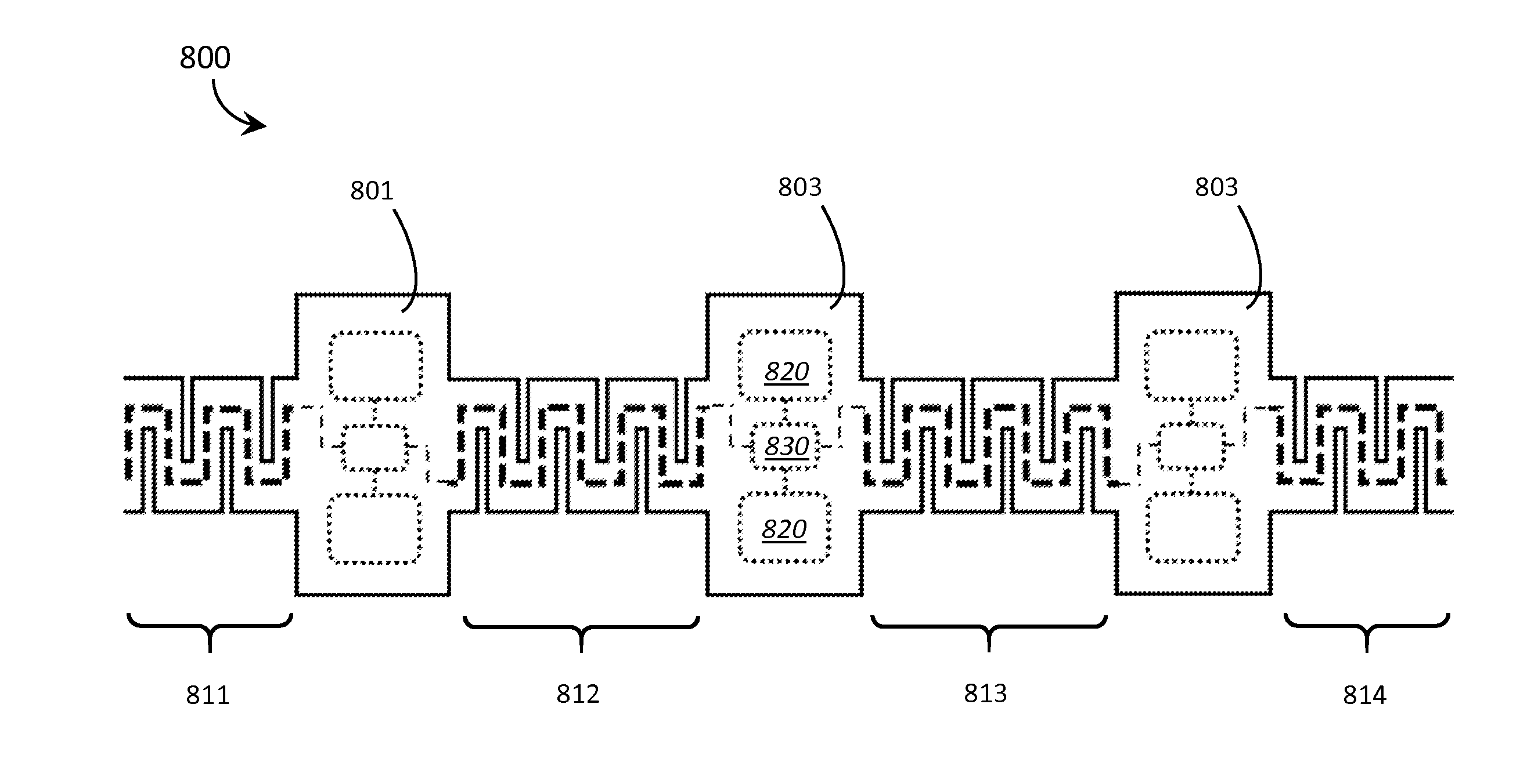
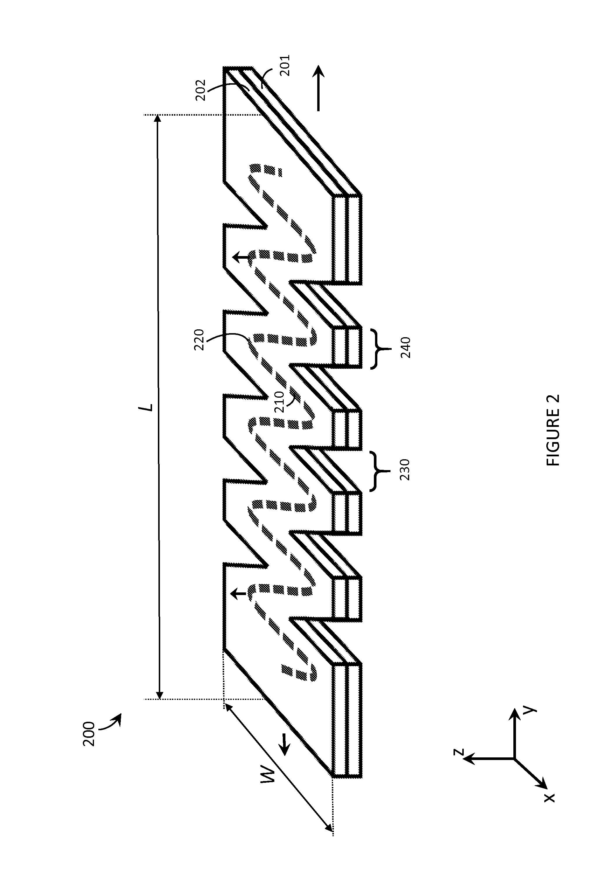

Stretchable film assembly with conductive traces
PatentActiveUS12124035B2
Innovation
- A stretchable film assembly with conductive traces and a dielectric film featuring a structured undulating or wavy profile, where both the conductive traces and dielectric film conform to alternating ridges and grooves, allowing them to experience tension equally in a stretched state, thereby reducing delamination and enabling stretching up to 2 to 5 times the original length.


Manufacturing Standards for Flexible Electronics Testing
The establishment of comprehensive manufacturing standards for flexible electronics testing has become increasingly critical as the industry transitions from laboratory prototypes to commercial applications. Current standardization efforts focus on developing unified protocols that can accurately assess the mechanical and electrical performance of flexible electronic devices under various deformation conditions. These standards must address the unique challenges posed by different trace geometries, particularly the comparative evaluation of wavy versus straight conductor patterns.
International standardization bodies, including IEC TC 119 and ASTM Committee F01, have initiated collaborative frameworks to define testing methodologies specific to flexible electronics. These efforts emphasize the need for standardized equipment specifications, environmental conditions, and measurement protocols that can provide reproducible results across different manufacturing facilities. The standards development process involves extensive validation studies comparing results from multiple testing laboratories to ensure measurement consistency.
Key testing parameters defined in emerging standards include strain rate specifications, temperature cycling protocols, and electrical continuity thresholds during mechanical deformation. For stretchability assessment, standards specify minimum sample sizes, substrate preparation methods, and fixture designs that accommodate both wavy and straight trace configurations. These protocols ensure that comparative studies between different trace geometries yield statistically significant and industrially relevant data.
Standardized test fixtures and measurement systems represent critical components of the manufacturing standards framework. Specifications define mechanical testing apparatus capable of applying controlled uniaxial and biaxial strains while simultaneously monitoring electrical resistance changes. The standards mandate calibration procedures for strain measurement systems and establish requirements for data acquisition sampling rates to capture transient electrical behavior during deformation cycles.
Quality assurance protocols embedded within manufacturing standards address statistical analysis methods for interpreting stretchability test results. These include requirements for sample population sizes, acceptable variance thresholds, and standardized reporting formats that facilitate cross-platform data comparison. The standards also establish pass/fail criteria based on application-specific performance requirements, enabling manufacturers to implement consistent quality control processes regardless of trace geometry selection.
Environmental Impact of Stretchable Electronics Materials
The environmental implications of stretchable electronics materials represent a critical consideration in the development and deployment of flexible electronic systems. As the industry moves toward more sustainable manufacturing practices, the choice between wavy and straight trace configurations significantly impacts the overall environmental footprint of printed electronics devices.
Material consumption patterns differ substantially between wavy and straight trace designs. Wavy configurations typically require additional conductive material to accommodate the serpentine patterns, resulting in increased raw material usage per unit area. This elevated consumption directly translates to higher environmental costs associated with mining, processing, and transportation of conductive inks and substrates. Conversely, straight traces optimize material efficiency but may necessitate more frequent device replacements due to reduced mechanical durability.
The manufacturing energy requirements vary considerably between these two approaches. Wavy trace production involves more complex printing processes, requiring precise control systems and extended processing times that increase energy consumption. The intricate patterning demands higher resolution printing equipment operating at reduced speeds, contributing to elevated carbon emissions per device. Straight trace manufacturing offers energy efficiency advantages through simplified production workflows and faster throughput rates.
Substrate selection plays a pivotal role in environmental impact assessment. Wavy designs often utilize specialized elastomeric substrates that provide enhanced mechanical compliance but may present challenges in end-of-life recycling. These materials frequently contain cross-linked polymers that resist conventional recycling processes. Straight trace implementations can leverage more environmentally friendly substrate options, including biodegradable polymers and recycled materials.
The lifecycle environmental assessment reveals distinct trade-offs between immediate manufacturing impacts and long-term sustainability. Wavy configurations demonstrate superior mechanical resilience, potentially extending device operational lifespans and reducing replacement frequency. This longevity factor can offset initial material and energy penalties through reduced cumulative environmental burden over the product lifecycle.
Waste generation patterns also differentiate these approaches. Manufacturing defect rates tend to be higher for wavy traces due to increased process complexity, resulting in greater material waste during production. However, the enhanced durability of wavy designs reduces electronic waste generation during the operational phase, presenting a complex environmental calculus that requires comprehensive lifecycle analysis to fully evaluate.
Unlock deeper insights with PatSnap Eureka Quick Research — get a full tech report to explore trends and direct your research. Try now!
Generate Your Research Report Instantly with AI Agent
Supercharge your innovation with PatSnap Eureka AI Agent Platform!