

How to Evaluate Backside Power Delivery in RF Modules
MAR 18, 202610 MIN READ
Generate Your Research Report Instantly with AI Agent
PatSnap Eureka helps you evaluate technical feasibility & market potential.
RF Module Backside Power Delivery Background and Objectives
Radio Frequency (RF) modules have undergone significant evolution since their inception in the early days of wireless communication systems. Initially, these modules relied primarily on frontside power delivery architectures, where power distribution networks were implemented on the same side as the active circuitry. However, as RF applications expanded into higher frequency bands and demanded greater power efficiency, the limitations of traditional power delivery methods became increasingly apparent.
The transition toward backside power delivery represents a paradigm shift in RF module design philosophy. This approach involves routing power supply networks through the substrate's backside, creating a dedicated power delivery pathway that is physically separated from the signal processing circuits. The concept emerged from the semiconductor industry's continuous pursuit of miniaturization and performance optimization, particularly as 5G networks and millimeter-wave applications demanded unprecedented levels of integration density.
Historical development patterns reveal that backside power delivery gained momentum around 2015-2018, coinciding with the industry's preparation for 5G deployment. Early implementations focused primarily on digital processors and system-on-chip designs, but the benefits quickly became evident for RF applications. The technology has since evolved through multiple generations, with each iteration addressing specific challenges related to thermal management, electromagnetic interference, and manufacturing complexity.
Current market drivers for backside power delivery in RF modules stem from several converging factors. The proliferation of Internet of Things devices requires compact, energy-efficient RF solutions that can operate reliably in diverse environments. Automotive radar systems operating at 77-81 GHz demand exceptional noise performance and thermal stability. Satellite communication systems require robust power delivery architectures capable of withstanding extreme operating conditions while maintaining signal integrity.
The primary technical objectives of implementing backside power delivery in RF modules center on achieving superior electrical performance through reduced parasitic effects. By segregating power distribution from signal paths, designers can minimize crosstalk, reduce ground bounce, and improve overall system stability. Thermal management represents another critical objective, as backside architectures enable more effective heat dissipation pathways, particularly important for high-power RF applications.
Performance optimization goals extend beyond basic functionality to encompass advanced metrics such as phase noise reduction, spurious signal suppression, and dynamic range enhancement. These objectives align with industry requirements for next-generation wireless systems that must operate with increasing spectral efficiency and reliability standards.
Manufacturing and cost considerations also drive the adoption of backside power delivery architectures. While initial implementation may require additional process steps, the long-term benefits include reduced board complexity, improved yield rates, and enhanced product reliability, ultimately contributing to lower total cost of ownership for RF system manufacturers.
Market Demand for Advanced RF Module Power Solutions
The global RF module market is experiencing unprecedented growth driven by the proliferation of 5G networks, Internet of Things applications, and advanced wireless communication systems. This expansion has created substantial demand for sophisticated power delivery solutions that can support increasingly complex RF architectures while maintaining signal integrity and thermal performance.
Mobile device manufacturers are pushing for higher integration density and improved power efficiency in RF front-end modules. The transition to 5G technology requires RF modules to handle multiple frequency bands simultaneously, creating new challenges for power distribution networks. Traditional front-side power delivery approaches are reaching their physical limitations as module complexity increases and available board space decreases.
Automotive electronics represents another significant growth driver, with vehicle electrification and autonomous driving systems requiring robust RF communication capabilities. These applications demand RF modules with enhanced reliability and thermal management, making advanced power delivery architectures essential for meeting automotive qualification standards.
The telecommunications infrastructure sector is investing heavily in base station equipment upgrades to support 5G deployment. This infrastructure modernization requires high-performance RF modules capable of handling increased power levels while maintaining efficiency across wide operating ranges. Backside power delivery solutions offer potential advantages in thermal management and electromagnetic isolation for these demanding applications.
Data center and cloud computing markets are also contributing to RF module demand growth. Edge computing deployments require compact, efficient RF solutions for wireless backhaul and connectivity applications. The need for higher data throughput and lower latency is driving requirements for more sophisticated power management approaches in RF module designs.
Consumer electronics manufacturers are seeking RF modules with improved battery life and reduced form factors. Wearable devices, smart home appliances, and portable communication equipment all require optimized power delivery solutions to meet consumer expectations for performance and battery longevity.
The aerospace and defense sectors continue to demand high-reliability RF modules for communication and radar applications. These markets require advanced power delivery solutions that can operate reliably in harsh environments while meeting stringent performance specifications. Backside power delivery architectures may offer advantages in terms of electromagnetic shielding and thermal dissipation for these critical applications.
Current State and Challenges in Backside Power Evaluation
The evaluation of backside power delivery in RF modules represents a critical yet technically challenging aspect of modern semiconductor design. Current industry practices predominantly rely on traditional front-side power distribution networks, where power delivery infrastructure is integrated within the same substrate layers as signal routing. This conventional approach has served the industry well for decades but increasingly faces limitations as RF modules demand higher power densities and improved performance metrics.
Existing evaluation methodologies primarily focus on impedance measurements, voltage ripple analysis, and thermal characterization through front-side access points. However, these techniques provide limited visibility into the actual power delivery performance at the device level, particularly when power is supplied through the substrate backside. The lack of standardized measurement protocols specifically designed for backside power evaluation creates significant gaps in performance validation and optimization processes.
One of the most significant technical challenges lies in the accessibility constraints inherent to backside power delivery systems. Unlike front-side configurations where test points and measurement access can be readily incorporated into the design, backside implementations often require specialized probing techniques and equipment. The substrate thickness and material properties introduce additional measurement complexities, making it difficult to accurately assess voltage regulation, current distribution uniformity, and dynamic response characteristics.
Thermal management presents another critical challenge in backside power evaluation. The heat dissipation pathways in backside power delivery configurations differ substantially from traditional approaches, requiring new thermal modeling techniques and measurement methodologies. Current thermal evaluation tools often lack the spatial resolution and accuracy needed to characterize the complex thermal interactions between power delivery networks and RF circuit elements in three-dimensional substrate configurations.
Signal integrity considerations add further complexity to the evaluation process. The electromagnetic coupling between backside power delivery networks and RF signal paths can significantly impact module performance, yet existing evaluation frameworks inadequately address these interactions. Traditional power integrity analysis tools were not designed to handle the unique electromagnetic environment created by backside power delivery implementations, leading to potential blind spots in performance characterization.
The industry currently lacks comprehensive simulation models that accurately represent the electrical, thermal, and electromagnetic behavior of backside power delivery systems. Existing modeling approaches often rely on simplified assumptions that may not capture the full complexity of substrate-integrated power networks, particularly in high-frequency RF applications where parasitic effects become increasingly significant.
Measurement equipment limitations further constrain evaluation capabilities. Standard power delivery test equipment was primarily developed for front-side access scenarios, and adapting these tools for backside evaluation often requires custom fixtures and specialized techniques that may introduce measurement uncertainties. The development of dedicated test methodologies and equipment specifically optimized for backside power delivery evaluation remains an ongoing industry need.
Existing Evaluation Methods for Backside Power Systems
01 Backside power delivery network architecture and routing
This category focuses on the fundamental architecture and design of backside power delivery networks in semiconductor devices. It includes methods for routing power rails, configuring power distribution networks on the backside of substrates, and establishing electrical connections between backside power networks and active device regions. The techniques involve strategic placement of power vias, interconnect structures, and metallization layers to enable efficient power delivery from the backside while minimizing resistance and improving current distribution across the chip.- Backside power delivery network architecture and routing: Backside power delivery involves designing power distribution networks on the backside of semiconductor dies to improve power delivery efficiency. This architecture includes routing power rails, power vias, and interconnects on the non-active side of the chip. The backside power delivery network can reduce IR drop, minimize power noise, and improve overall power integrity by providing dedicated power paths separate from signal routing layers.
- Backside power delivery with through-silicon vias: Through-silicon vias are utilized in backside power delivery implementations to establish electrical connections between the backside power network and the active circuitry on the front side. These vertical interconnects enable efficient power transfer while maintaining compact die dimensions. The integration of through-silicon vias in backside power delivery structures allows for reduced resistance paths and improved current carrying capacity.
- Backside power delivery with buried power rails: Buried power rails are implemented beneath the active device layer to provide backside power delivery. This approach involves forming power distribution structures within the substrate or in dedicated layers below the transistor level. The buried power rail configuration enables higher power delivery density and reduces the impact on front-side routing resources, allowing for more efficient use of metal layers for signal interconnects.
- Thermal management in backside power delivery: Thermal management techniques are integrated with backside power delivery structures to address heat dissipation challenges. The backside power delivery configuration can facilitate improved thermal paths by utilizing the substrate and backside metallization for heat spreading. Thermal interface materials and heat sinks can be more effectively coupled to the backside power delivery network to enhance cooling efficiency and maintain optimal operating temperatures.
- Hybrid power delivery combining frontside and backside approaches: Hybrid power delivery architectures combine both frontside and backside power distribution networks to optimize power delivery performance. This approach leverages the advantages of both configurations by distributing power delivery responsibilities between the front and back sides of the die. The hybrid implementation allows for flexible power domain partitioning, improved voltage regulation, and enhanced power delivery to high-performance circuit blocks while maintaining compatibility with existing design methodologies.
02 Backside power delivery with through-silicon vias and substrate modifications
This approach involves the use of through-silicon vias and substrate engineering techniques to implement backside power delivery. It encompasses methods for forming deep trench structures, creating conductive pathways through the substrate, and modifying substrate properties to facilitate power distribution. The techniques address challenges related to substrate thinning, via formation, and integration of backside power networks with frontside circuitry while maintaining structural integrity and electrical performance.Expand Specific Solutions03 Hybrid power delivery combining frontside and backside networks
This category covers integrated solutions that combine both frontside and backside power delivery mechanisms. It includes techniques for partitioning power distribution between the two sides, coordinating voltage domains, and optimizing the allocation of power resources. The methods address how to balance power delivery requirements, reduce IR drop, and improve overall power efficiency by leveraging the advantages of both frontside and backside power distribution approaches in a complementary manner.Expand Specific Solutions04 Backside power delivery for advanced packaging and 3D integration
This focuses on backside power delivery implementations in advanced packaging configurations and three-dimensional integrated circuits. It includes techniques for multi-die stacking, chiplet integration, and heterogeneous integration where backside power delivery enables improved power distribution across multiple layers or components. The approaches address thermal management, inter-die connectivity, and power network coordination in complex 3D structures while maintaining signal integrity and reducing package complexity.Expand Specific Solutions05 Process integration and manufacturing methods for backside power delivery
This category encompasses manufacturing processes and integration schemes specifically developed for implementing backside power delivery structures. It includes wafer processing techniques, metallization methods, dielectric layer formation, and process flows that enable the fabrication of backside power networks. The techniques address challenges in process compatibility, yield optimization, and cost-effective manufacturing while ensuring reliable electrical connections and mechanical stability of the backside power delivery infrastructure.Expand Specific Solutions
Key Players in RF Module and Power Delivery Industry
The backside power delivery evaluation in RF modules represents a rapidly evolving technological domain driven by increasing demands for miniaturization and performance optimization in wireless communications. The market is experiencing significant growth as 5G deployment accelerates and IoT applications proliferate, creating substantial opportunities for specialized solutions. Technology maturity varies considerably across market participants, with established semiconductor leaders like Qualcomm, Intel, and Samsung Electronics demonstrating advanced capabilities through extensive R&D investments and comprehensive product portfolios. RF specialists including Skyworks Solutions and Cirrus Logic have developed sophisticated evaluation methodologies and measurement techniques. Meanwhile, equipment manufacturers such as Applied Materials, Lam Research, and MKS provide critical testing infrastructure. Chinese companies like Huawei, ZTE, and Vanchip are rapidly advancing their technological capabilities, while foundry leaders like TSMC enable cutting-edge implementations. The competitive landscape reflects a maturing industry with established players maintaining technological leadership while emerging companies drive innovation in specialized applications.
Skyworks Solutions, Inc.
Technical Solution: Skyworks has developed comprehensive backside power delivery evaluation methodologies for RF modules, focusing on thermal management and power integrity analysis. Their approach includes advanced substrate technologies with integrated power planes, utilizing low-loss dielectric materials and optimized via structures. The company employs sophisticated simulation tools to model power distribution networks (PDN) impedance characteristics and thermal dissipation patterns. Their evaluation framework incorporates real-time power consumption monitoring, thermal imaging analysis, and electromagnetic interference assessment to ensure optimal performance in mobile and IoT applications.
Strengths: Industry-leading RF expertise with proven track record in mobile applications, comprehensive thermal management solutions. Weaknesses: Limited focus on emerging applications beyond mobile communications, higher cost solutions.
Samsung Electronics Co., Ltd.
Technical Solution: Samsung's backside power delivery evaluation methodology combines their semiconductor manufacturing expertise with advanced packaging technologies. Their approach utilizes fan-out wafer-level packaging (FOWLP) and system-in-package (SiP) technologies to optimize power distribution in RF modules. The evaluation framework includes comprehensive power integrity analysis using time-domain and frequency-domain measurements, thermal characterization through advanced thermal interface materials, and electromagnetic compatibility testing. Samsung employs machine learning algorithms to optimize power delivery network design based on performance requirements and manufacturing constraints, enabling efficient evaluation and optimization of RF module power systems.
Strengths: Advanced manufacturing capabilities, innovative packaging technologies, strong integration of AI/ML in design optimization. Weaknesses: Limited availability of technologies to external customers, focus primarily on consumer electronics applications.
Core Innovations in RF Backside Power Assessment
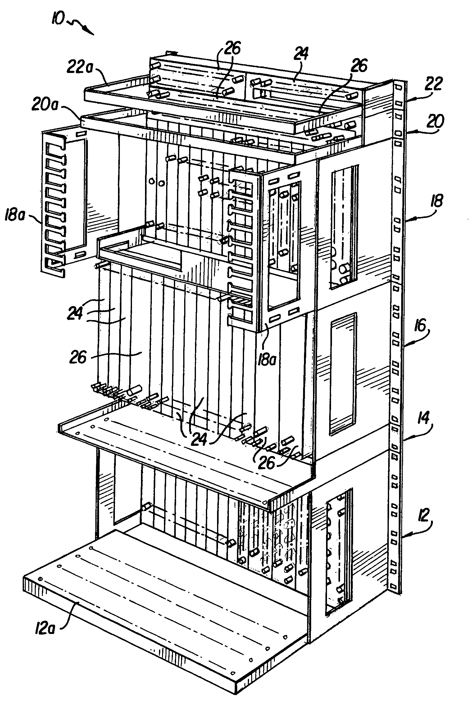
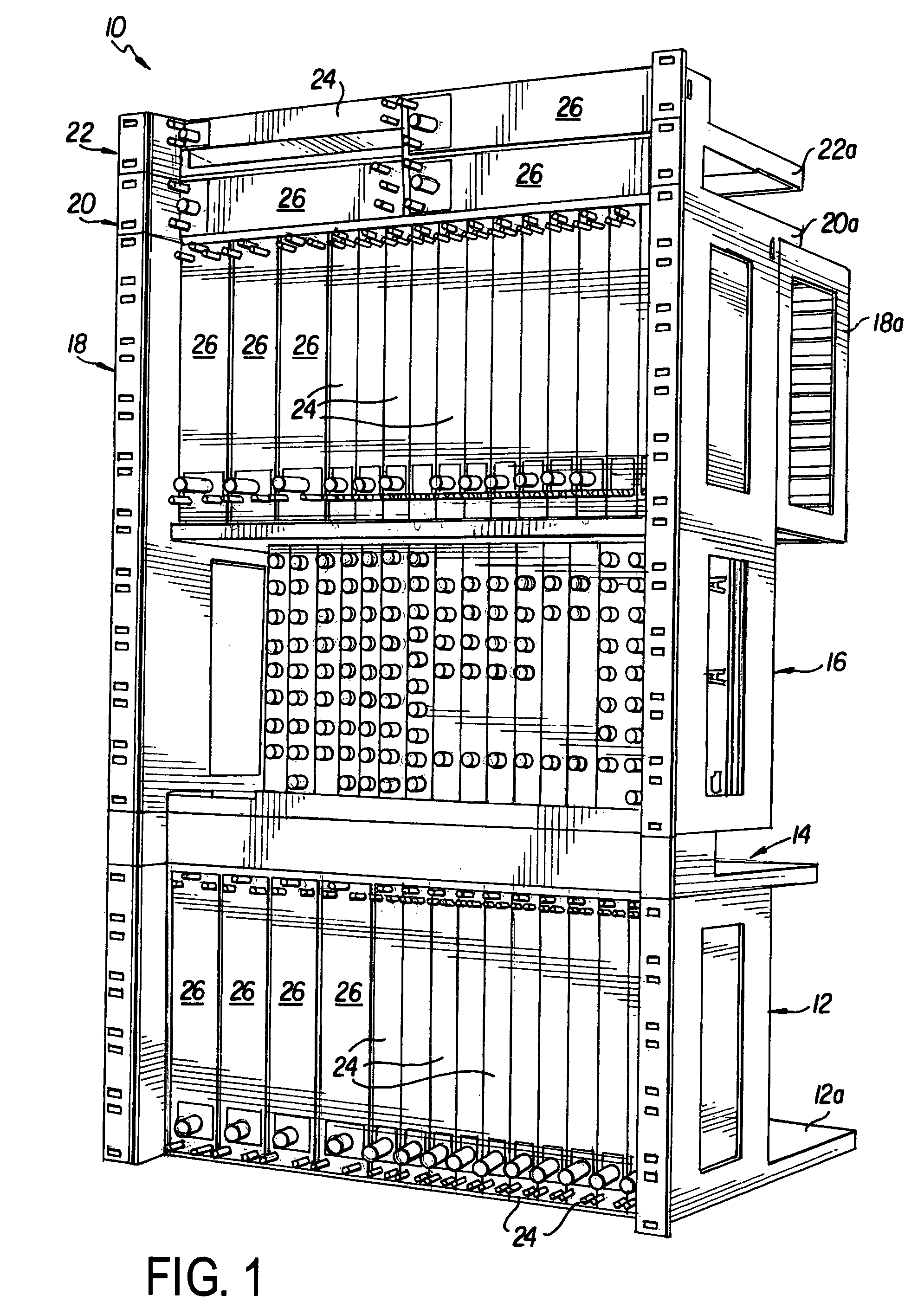
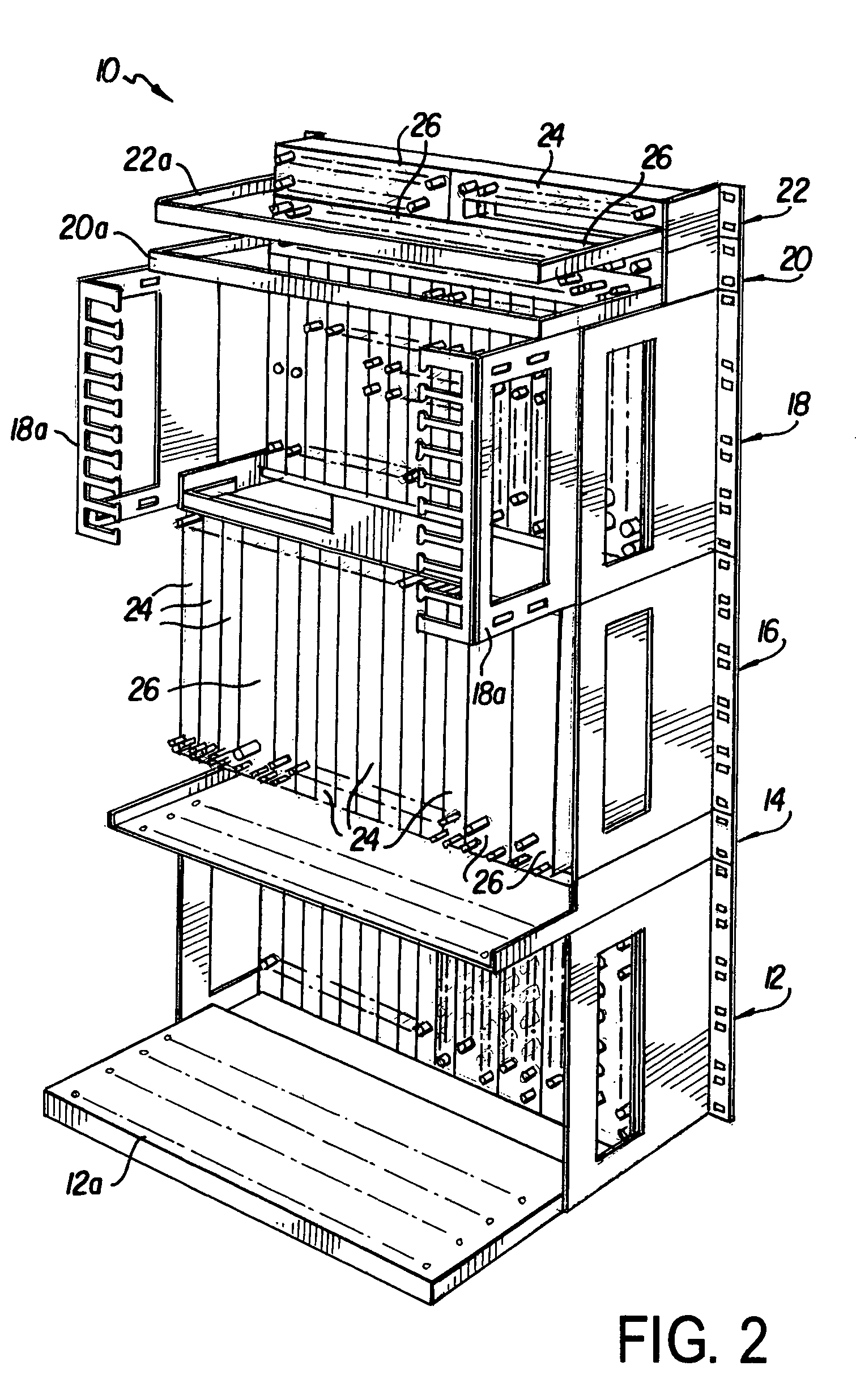
RF circuit modules and integrated chassis with power interface for RF circuit modules
PatentActiveUS7855896B2
Innovation
- A modular RF management system featuring a rack-mountable chassis with an integrated power bus, capable of hosting both active and passive RF modules, along with 'hot-swappable' power supply modules and various cable management structures, allowing for flexible configuration and reconfiguration to suit different requirements.

Single transmission line for connecting radio frequency modules in an electronic device
PatentActiveUS9496948B2
Innovation
- A single transmission line is used to multiplex and demultiplex intermediate frequency, local oscillator, control, and power signals between baseband and RF modules, utilizing a metal line on a multilayer substrate and interface units to enable efficient signal transfer over distance, reducing the need for multiple cables and minimizing signal loss.


EMC Compliance Standards for RF Power Systems
Electromagnetic compatibility (EMC) compliance represents a critical regulatory framework governing RF power systems, particularly those incorporating backside power delivery architectures. The fundamental standards encompass conducted and radiated emissions limits, immunity requirements, and harmonic distortion thresholds that directly impact power delivery network design. Key regulatory bodies including FCC, CISPR, and IEC establish stringent guidelines for RF modules operating across various frequency bands, with specific attention to power delivery subsystems that may introduce unwanted electromagnetic interference.
The primary EMC standards applicable to RF power systems include CISPR 22 for information technology equipment emissions, IEC 61000-4 series for immunity testing, and FCC Part 15 for unlicensed RF devices. These standards define measurement methodologies, test configurations, and acceptable limits for both narrowband and broadband emissions originating from power delivery networks. Backside power delivery implementations must demonstrate compliance across multiple test scenarios, including normal operation, transient conditions, and various load configurations.
Conducted emissions testing focuses on power line disturbances generated by switching regulators and DC-DC converters commonly employed in backside power architectures. The standards specify measurement bandwidth, detector functions, and quasi-peak limits ranging from 150 kHz to 30 MHz for conducted emissions. RF modules utilizing backside power delivery must implement appropriate filtering and isolation techniques to meet these stringent requirements while maintaining power delivery efficiency and thermal performance.
Radiated emissions compliance presents additional challenges for backside power delivery systems, as power distribution networks can act as unintentional antennas. Standards define far-field measurement distances, antenna polarizations, and frequency sweep parameters for emissions testing from 30 MHz to several GHz. The proximity of power delivery components to RF circuitry in backside architectures requires careful electromagnetic isolation and shielding strategies to prevent coupling between power and signal domains.
Immunity standards address the system's ability to maintain functionality under external electromagnetic stress. IEC 61000-4-3 radiated immunity testing and IEC 61000-4-6 conducted immunity requirements establish performance criteria for RF power systems exposed to interfering signals. Backside power delivery networks must demonstrate stable operation and maintain regulation accuracy when subjected to these standardized interference scenarios, ensuring reliable performance in real-world electromagnetic environments.
Thermal Management Considerations in RF Power Design
Thermal management represents one of the most critical aspects in RF power design, particularly when evaluating backside power delivery systems in RF modules. The increasing power densities and miniaturization trends in modern RF applications have elevated thermal considerations from secondary concerns to primary design constraints that directly impact system performance, reliability, and longevity.
The fundamental challenge in RF power design stems from the inherent inefficiencies in power conversion and amplification processes. When RF modules operate at high power levels, significant amounts of energy are dissipated as heat, creating localized hot spots that can degrade performance and potentially cause catastrophic failures. Backside power delivery architectures, while offering advantages in terms of signal integrity and electromagnetic interference reduction, introduce unique thermal pathways that must be carefully analyzed and optimized.
Junction temperature control emerges as the paramount concern in RF power design. Semiconductor devices, particularly gallium arsenide and gallium nitride components commonly used in high-frequency applications, exhibit strong temperature dependencies in their electrical characteristics. Elevated operating temperatures can lead to reduced gain, increased noise figure, frequency drift, and accelerated aging mechanisms that compromise long-term reliability.
Thermal resistance modeling becomes essential for accurate performance prediction in backside power delivery configurations. The thermal path from the active junction through the substrate, thermal interface materials, and heat spreading structures must be characterized with precision. This modeling process requires consideration of both steady-state and transient thermal behaviors, as RF applications often involve pulsed or modulated power profiles that create dynamic thermal conditions.
Heat spreading techniques play a crucial role in managing thermal challenges in RF modules. Advanced thermal interface materials, including phase-change materials and liquid metal interfaces, offer improved thermal conductivity compared to traditional solutions. Additionally, integrated heat spreaders and thermal vias provide efficient pathways for heat extraction from critical components to external cooling systems.
Package-level thermal design considerations encompass material selection, geometric optimization, and integration with system-level cooling solutions. The coefficient of thermal expansion matching between different materials becomes critical to prevent mechanical stress and maintain thermal interface integrity over temperature cycling. Furthermore, the thermal design must accommodate the specific requirements of backside power delivery, ensuring that power distribution networks do not create thermal bottlenecks or interfere with heat extraction pathways.
Unlock deeper insights with PatSnap Eureka Quick Research — get a full tech report to explore trends and direct your research. Try now!
Generate Your Research Report Instantly with AI Agent
Supercharge your innovation with PatSnap Eureka AI Agent Platform!