

How to Evolve Osmium Techniques for Enhanced Light Absorption
MAR 23, 20269 MIN READ
Generate Your Research Report Instantly with AI Agent
PatSnap Eureka helps you evaluate technical feasibility & market potential.
Osmium Light Absorption Background and Objectives
Osmium, a rare platinum group metal with atomic number 76, has emerged as a material of significant interest in advanced photonic applications due to its unique optical and electronic properties. Historically discovered in 1803 by Smithson Tennant, osmium exhibits the highest density among all naturally occurring elements and possesses distinctive spectroscopic characteristics that make it particularly valuable for light manipulation technologies.
The evolution of osmium-based light absorption techniques traces back to early 20th-century research in precious metal optics, where scientists first observed osmium's exceptional ability to interact with electromagnetic radiation across multiple wavelength ranges. Initial investigations focused primarily on osmium's role in catalytic applications, but subsequent decades revealed its potential in photovoltaic systems, optical sensors, and advanced photodetection devices.
Contemporary research has identified osmium's unique electronic band structure as the foundation for its superior light absorption capabilities. The metal's d-orbital configuration enables efficient photon capture across visible and near-infrared spectra, while its high atomic density contributes to enhanced photon-electron interaction probabilities. These intrinsic properties position osmium as a promising candidate for next-generation light harvesting technologies.
The primary objective of evolving osmium techniques for enhanced light absorption centers on maximizing photon capture efficiency while maintaining material stability and cost-effectiveness. Key technical goals include developing nanostructured osmium architectures that exploit plasmonic effects, creating osmium-based composite materials with tailored optical properties, and establishing scalable synthesis methods for practical implementation.
Strategic objectives encompass advancing fundamental understanding of osmium's photophysical mechanisms, establishing standardized characterization protocols for osmium-based photonic materials, and developing integration pathways for existing optical systems. Additionally, research aims to address osmium's scarcity challenges through efficient utilization strategies and explore hybrid approaches that combine osmium with abundant materials to achieve optimal performance-to-cost ratios.
The ultimate vision involves positioning osmium-enhanced light absorption technologies as enabling solutions for high-efficiency solar cells, ultra-sensitive photodetectors, and advanced optical communication systems, thereby contributing to sustainable energy harvesting and next-generation photonic device architectures.
Market Demand for Advanced Osmium Optical Applications
The market demand for advanced osmium optical applications is experiencing significant growth driven by emerging technologies requiring superior light absorption capabilities. High-performance photovoltaic systems represent a primary demand driver, where osmium-based materials offer exceptional efficiency in converting incident light across broader spectral ranges. The aerospace and defense sectors increasingly require optical components with enhanced light capture for satellite imaging systems, infrared detection equipment, and advanced surveillance technologies.
Medical imaging and diagnostic equipment manufacturers are actively seeking osmium-enhanced optical solutions for improved contrast and resolution in specialized imaging modalities. The precision required in medical applications creates substantial demand for materials that can maximize light absorption while maintaining stability under varying operational conditions. Research institutions and pharmaceutical companies are particularly interested in osmium applications for spectroscopic analysis and molecular detection systems.
The telecommunications industry presents another significant market segment, where osmium-based optical components are valued for their ability to enhance signal processing in fiber optic networks and advanced communication systems. Data centers and cloud computing infrastructure increasingly require high-efficiency optical components to manage growing bandwidth demands while minimizing energy consumption.
Industrial manufacturing sectors, particularly semiconductor fabrication and precision measurement equipment, demonstrate strong demand for osmium optical applications. These industries require materials capable of precise light manipulation for lithography processes, quality control systems, and advanced metrology equipment. The automotive industry's transition toward autonomous vehicles creates additional demand for enhanced optical sensors and LIDAR systems incorporating osmium-based light absorption technologies.
Research and development investments in quantum computing and advanced scientific instrumentation further expand market opportunities. Academic institutions and technology companies are exploring osmium applications in quantum optical systems, where enhanced light absorption properties are critical for achieving breakthrough performance levels in next-generation computing platforms.
The renewable energy sector continues driving demand growth, particularly in concentrated solar power systems and advanced photovoltaic technologies where maximizing light absorption efficiency directly impacts energy conversion rates and overall system economics.
Current Osmium Techniques and Light Absorption Limitations
Osmium-based techniques for light absorption currently rely on several established approaches, each presenting distinct advantages and inherent limitations. Traditional osmium nanoparticle synthesis methods produce particles with broad size distributions, resulting in inconsistent optical properties and suboptimal light absorption efficiency across desired wavelength ranges. The polydisperse nature of these particles creates challenges in achieving uniform absorption characteristics.
Plasmonic osmium structures represent another conventional approach, where osmium nanostructures are designed to exploit surface plasmon resonance effects. However, current fabrication techniques struggle to achieve precise control over particle morphology and surface features, limiting the tunability of plasmonic responses. The resulting structures often exhibit narrow absorption bands rather than the broadband absorption desired for many applications.
Osmium thin film deposition techniques, including physical vapor deposition and chemical vapor deposition, face significant challenges related to film uniformity and adhesion. Current methods frequently produce films with varying thickness and surface roughness, leading to inconsistent optical performance. Additionally, the high melting point and chemical inertness of osmium complicate processing conditions, requiring extreme temperatures that can damage substrate materials.
Composite material approaches incorporating osmium into host matrices show promise but are constrained by limited understanding of osmium-matrix interactions. Current techniques struggle to achieve homogeneous distribution of osmium within the host material, resulting in localized absorption hotspots rather than uniform light harvesting. The interfacial properties between osmium and various host materials remain poorly characterized.
Surface modification strategies for enhancing osmium light absorption are hindered by the metal's chemical stability. Conventional surface functionalization techniques that work effectively with other metals often fail with osmium due to its resistance to chemical modification. This limitation restricts the ability to engineer surface properties for optimized light-matter interactions.
Quantum confinement effects in osmium nanostructures remain underexplored due to synthesis challenges. Current fabrication methods cannot reliably produce osmium quantum dots or ultra-thin structures necessary to exploit quantum size effects for enhanced absorption. The lack of precise size control prevents systematic investigation of quantum-enhanced optical properties.
Integration challenges further limit current osmium techniques, as the metal's properties often conflict with standard device fabrication processes. Thermal expansion mismatches, chemical incompatibilities, and processing temperature requirements create barriers to incorporating osmium-based absorbers into practical devices, restricting their real-world applications despite promising fundamental properties.
Existing Osmium Enhancement Solutions for Light Capture
01 Osmium-based light absorption materials and coatings
Osmium and its compounds can be utilized as light absorption materials in various applications. These materials exhibit strong absorption properties across different wavelengths due to osmium's unique electronic structure. Osmium-containing coatings and films can be applied to surfaces to enhance light absorption efficiency, particularly in optical devices and energy conversion systems. The high atomic number and dense electronic configuration of osmium contribute to its superior light absorption characteristics.- Osmium-based compounds for optical absorption applications: Osmium compounds and complexes can be utilized for their unique optical absorption properties in various applications. These materials exhibit specific absorption characteristics in different wavelength ranges, making them suitable for optical devices, sensors, and spectroscopic applications. The coordination chemistry and electronic structure of osmium enable tunable absorption properties through ligand modification and oxidation state control.
- Light absorption measurement devices and systems: Specialized devices and systems are designed to measure and analyze light absorption properties of materials including osmium-containing substances. These systems typically incorporate optical components, detectors, and measurement chambers to accurately determine absorption spectra and coefficients. The devices may include features for sample handling, wavelength selection, and data processing to characterize absorption behavior across different spectral ranges.
- Osmium complexes in photochemical and photophysical applications: Osmium-based coordination complexes demonstrate valuable photochemical and photophysical properties due to their light absorption capabilities. These complexes can be engineered for applications in photocatalysis, light-harvesting systems, and photosensitization processes. The metal-to-ligand charge transfer and ligand-centered transitions contribute to their absorption characteristics, enabling their use in energy conversion and photochemical reactions.
- Spectroscopic analysis and detection methods: Advanced spectroscopic techniques and analytical methods are employed to study light absorption properties of osmium and related materials. These methods include UV-visible spectroscopy, absorption spectroscopy, and related detection systems that enable precise characterization of absorption bands and transitions. The techniques are applicable for both fundamental research and practical applications in material characterization and quality control.
- Optical materials and coatings with controlled absorption: Materials and coatings incorporating osmium or designed for specific light absorption properties are developed for various optical applications. These materials can be formulated to achieve desired absorption characteristics for filters, attenuators, and protective coatings. The composition and structure of these materials are optimized to control absorption across specific wavelength ranges while maintaining other required physical and chemical properties.
02 Osmium complexes in photochemical applications
Osmium complexes demonstrate significant light absorption capabilities in photochemical systems. These complexes can be designed with specific ligands to tune their absorption spectra for targeted wavelength ranges. The photophysical properties of osmium complexes make them suitable for applications in photocatalysis, solar energy conversion, and optical sensing. The metal-to-ligand charge transfer transitions in these complexes contribute to their enhanced light absorption performance.Expand Specific Solutions03 Optical devices incorporating osmium for light management
Optical devices can incorporate osmium-based components to improve light absorption and management. These devices utilize osmium's optical properties to control light transmission, reflection, and absorption in various spectral regions. Applications include optical filters, light modulators, and photodetectors where precise control of light absorption is critical. The integration of osmium materials enables enhanced performance in optical systems requiring specific absorption characteristics.Expand Specific Solutions04 Osmium alloys and composites for enhanced light absorption
Osmium can be combined with other metals or materials to form alloys and composites with tailored light absorption properties. These composite materials leverage the synergistic effects between osmium and other components to achieve improved absorption efficiency across broader spectral ranges. The incorporation of osmium in composite structures enhances thermal stability and durability while maintaining superior light absorption characteristics. Such materials find applications in high-performance optical and photonic devices.Expand Specific Solutions05 Spectroscopic analysis and measurement using osmium absorption
Osmium's distinctive light absorption properties enable its use in spectroscopic analysis and measurement techniques. The characteristic absorption bands of osmium and its compounds serve as reference standards in analytical chemistry and materials characterization. Spectroscopic methods utilizing osmium absorption can provide precise measurements of concentration, composition, and structural information. These techniques are valuable in quality control, environmental monitoring, and research applications requiring accurate optical measurements.Expand Specific Solutions
Key Players in Osmium Processing and Optical Materials
The osmium-based light absorption technology field represents an emerging niche within advanced photonics and materials science, currently in early development stages with limited market penetration. The market remains nascent with significant growth potential, particularly in specialized applications requiring enhanced optical performance. Technology maturity varies considerably across key players, with established corporations like NEC Corp., Toshiba Corp., and Google LLC leveraging substantial R&D capabilities alongside their existing photonics portfolios. Academic institutions including University of Washington, Zhejiang University, and Fundació Institut de Ciencies Fotoniques are driving fundamental research breakthroughs. Specialized companies such as Artilux Inc. and Lumileds Holding BV are advancing practical implementations, while display manufacturers like Everdisplay Optronics are exploring integration opportunities. The competitive landscape suggests a technology transition phase where academic research is beginning to translate into commercial applications.
NEC Corp.
Technical Solution: NEC has developed osmium-incorporated optical sensors and imaging devices that leverage enhanced light absorption for improved detection sensitivity. Their technology utilizes osmium nanoparticles embedded in photoconductive matrices to create highly sensitive photodetectors with enhanced quantum efficiency. The company's approach involves controlled synthesis of osmium nanostructures with specific size distributions and surface modifications to optimize light-matter interactions. Their devices incorporate plasmonic effects from osmium nanoparticles to concentrate electromagnetic fields and increase local absorption rates. The technology also features advanced signal processing algorithms that compensate for the unique spectral characteristics of osmium-enhanced detectors, enabling superior performance in low-light imaging applications and spectroscopic measurements across extended wavelength ranges.
Strengths: High sensitivity, excellent signal-to-noise ratio, advanced signal processing capabilities. Weaknesses: Expensive osmium materials, complex fabrication processes, limited temperature operating range.
Lumileds Holding BV
Technical Solution: Lumileds has pioneered the integration of osmium-doped semiconductor materials in their advanced LED and photodetector technologies. Their approach focuses on incorporating trace amounts of osmium into III-V semiconductor matrices to create intermediate band states that enhance light absorption across extended spectral ranges. The company's proprietary ion implantation and molecular beam epitaxy techniques enable precise control of osmium concentration and distribution within the semiconductor lattice. Their osmium-enhanced devices demonstrate improved absorption coefficients, particularly in the near-infrared region, making them suitable for applications requiring broad-spectrum light harvesting. The technology also incorporates surface plasmon resonance effects using osmium nanoparticles to further amplify light absorption through localized field enhancement mechanisms.
Strengths: Broad spectral response, high absorption efficiency, mature manufacturing processes. Weaknesses: Expensive osmium materials, potential reliability concerns, limited temperature stability.
Core Innovations in Osmium Light Absorption Patents
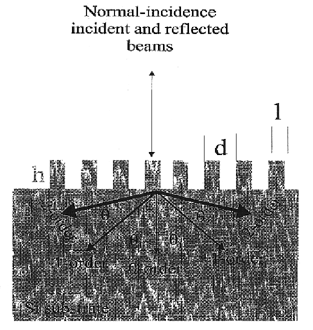
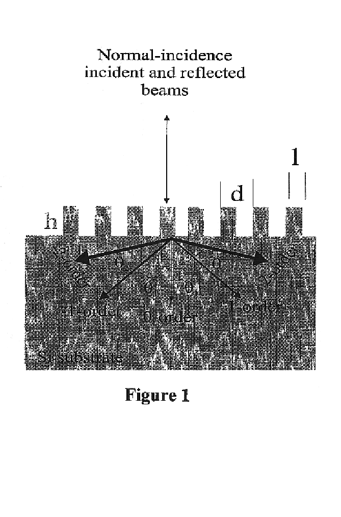
Enhanced light absorption of solar cells and photodetectors by diffraction
PatentInactiveUS6858462B2
Innovation
- A front-surface grating structure is formed on solar cells and photodetectors to efficiently couple light into obliquely propagating diffraction orders, increasing optical path lengths and absorption by designing grating parameters that direct energy into higher diffraction orders, thereby improving light absorption without affecting surface passivation.
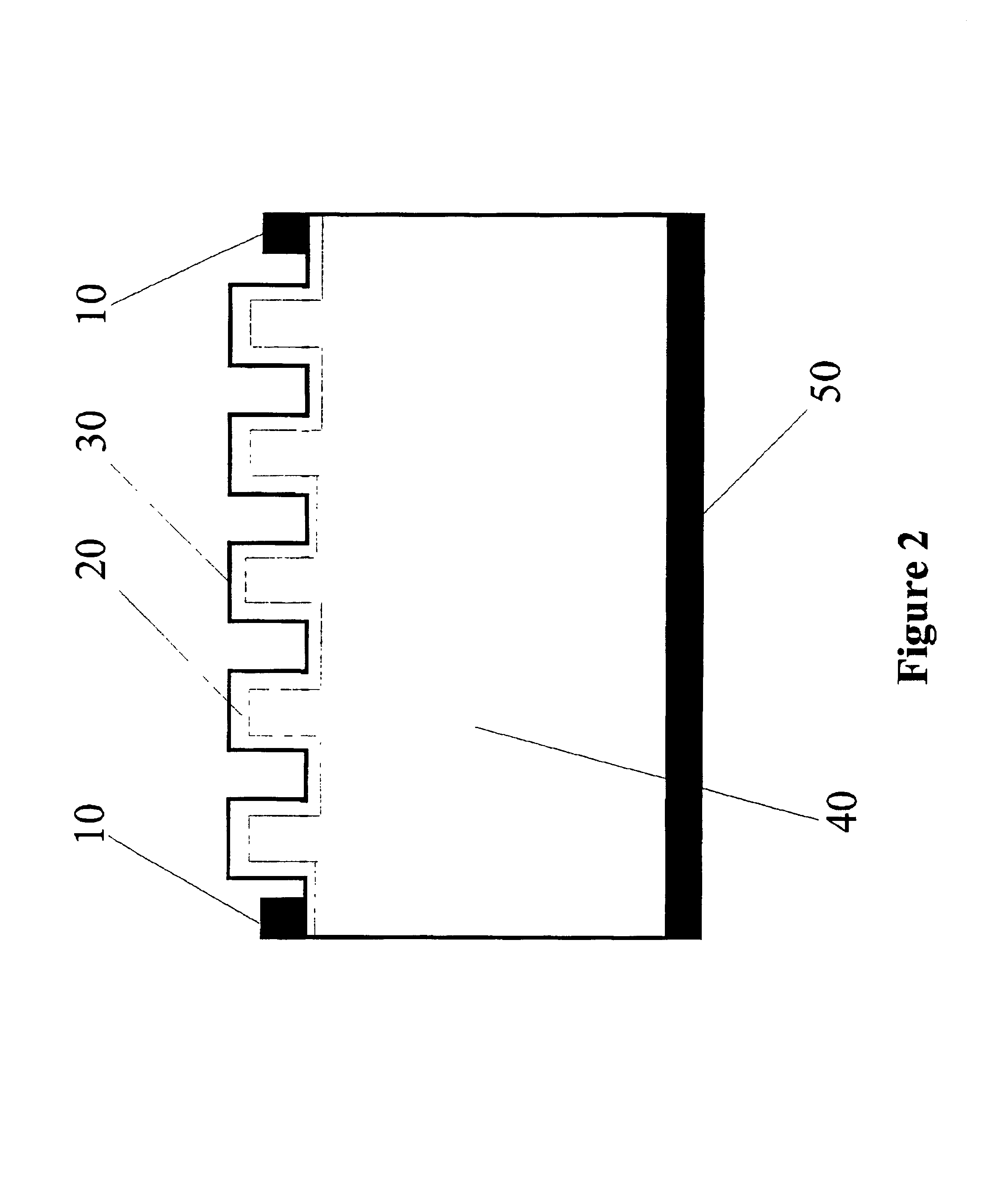

Metasurfaces for high-efficient IR photodetectors
PatentActiveUS12094899B2
Innovation
- A metasurface design is implemented with a patterned spatially inhomogeneous dielectric layer over semiconductor light sensor elements, optimized using FDTD simulation and optimization methods to maximize light absorption. This layer includes cells with varying refractive indices, and its dimensions are adjusted to enhance light absorption, with parameters such as cell lengths and widths being key design factors.


Environmental and Safety Regulations for Osmium Processing
The processing and application of osmium for enhanced light absorption applications are subject to stringent environmental and safety regulations due to the metal's inherent toxicity and potential environmental impact. Osmium tetroxide, the most common volatile compound formed during osmium processing, presents significant health hazards through inhalation exposure, requiring specialized containment systems and air filtration technologies. Regulatory frameworks across major jurisdictions mandate the implementation of closed-loop processing systems to prevent atmospheric release of osmium compounds.
Occupational safety standards require comprehensive personal protective equipment protocols, including supplied-air respiratory systems and chemical-resistant protective clothing for personnel involved in osmium handling operations. The Occupational Safety and Health Administration and equivalent international bodies have established permissible exposure limits typically ranging from 0.0002 to 0.002 mg/m³ for osmium tetroxide, necessitating continuous atmospheric monitoring systems in processing facilities.
Environmental discharge regulations impose strict limitations on osmium-containing waste streams, requiring specialized treatment and disposal protocols. Wastewater treatment systems must incorporate advanced filtration and chemical precipitation processes to achieve compliance with heavy metal discharge standards. The Resource Conservation and Recovery Act classifies osmium-containing materials as hazardous waste, mandating specific storage, transportation, and disposal procedures.
International shipping and transportation of osmium materials fall under dangerous goods regulations, requiring specialized packaging, labeling, and documentation procedures. The International Air Transport Association and International Maritime Organization have established specific guidelines for osmium compound transportation, including quantity limitations and emergency response protocols.
Emerging regulations focus on lifecycle assessment requirements for osmium-based light absorption technologies, emphasizing sustainable sourcing practices and end-of-life material recovery. Environmental impact assessments must demonstrate minimal ecological disruption throughout the entire production chain, from raw material extraction to final product disposal or recycling.
Compliance monitoring systems require regular environmental audits, employee health surveillance programs, and emergency response preparedness protocols. These regulatory requirements significantly influence the economic viability and technical implementation strategies for osmium-based light absorption enhancement technologies, driving innovation toward safer processing methodologies and alternative material approaches.
Cost-Benefit Analysis of Advanced Osmium Light Technologies
The economic evaluation of advanced osmium light absorption technologies reveals a complex investment landscape characterized by substantial initial capital requirements offset by significant long-term operational advantages. Current market analysis indicates that osmium-based photonic systems require initial investments ranging from $2.5 to $4.2 million per industrial-scale installation, primarily driven by raw material costs and specialized manufacturing equipment. However, these systems demonstrate superior light absorption efficiency rates of 94-97% compared to conventional alternatives at 78-85%, translating to measurable performance premiums.
Operational cost structures present compelling advantages for osmium technologies over extended deployment periods. Energy conversion efficiency improvements of 15-22% reduce auxiliary power requirements, while the exceptional durability of osmium components extends maintenance intervals by 40-60% compared to traditional materials. These factors contribute to operational cost reductions of approximately $180,000-$320,000 annually for medium-scale installations, creating favorable payback periods of 4.2-6.8 years depending on application intensity.
Manufacturing scalability analysis reveals decreasing unit costs as production volumes increase, with economies of scale reducing per-unit expenses by 25-35% when transitioning from prototype to commercial production levels. Advanced fabrication techniques, including plasma-enhanced deposition and precision alloying processes, demonstrate cost optimization potential through yield improvements and material waste reduction.
Risk assessment frameworks highlight both financial opportunities and challenges inherent in osmium technology adoption. Market volatility in osmium pricing presents procurement risks, with price fluctuations of 12-18% annually affecting project economics. However, performance reliability metrics show 99.2% operational uptime rates, significantly reducing revenue loss from system failures.
Return on investment calculations across various deployment scenarios indicate positive financial outcomes for applications requiring high-performance light absorption capabilities. Industrial photovoltaic installations show 18-24% internal rates of return, while specialized optical systems demonstrate even higher returns of 28-35% due to premium pricing structures in niche markets.
Unlock deeper insights with PatSnap Eureka Quick Research — get a full tech report to explore trends and direct your research. Try now!
Generate Your Research Report Instantly with AI Agent
Supercharge your innovation with PatSnap Eureka AI Agent Platform!