How to Maximize Backside Metallization Layers for Solar Panels
APR 15, 20269 MIN READ
Generate Your Research Report Instantly with AI Agent
PatSnap Eureka helps you evaluate technical feasibility & market potential.
Solar Panel Backside Metallization Background and Objectives
Solar panel backside metallization has emerged as a critical technology frontier in photovoltaic cell design, representing a paradigm shift from traditional front-contact architectures toward more sophisticated rear-contact configurations. This technological evolution stems from the fundamental limitations of conventional solar cell designs, where front-side metallization creates shadowing losses and restricts the active light-absorbing area. The development of backside metallization techniques addresses these constraints by relocating electrical contacts to the rear surface, thereby maximizing light capture efficiency.
The historical progression of backside metallization began with early point-contact solar cells in the 1980s, evolving through various iterations including passivated emitter and rear contact (PERC) cells, interdigitated back contact (IBC) designs, and more recently, tunnel oxide passivated contact (TOPCon) technologies. Each evolutionary step has demonstrated incremental improvements in power conversion efficiency, with modern backside metallization approaches achieving laboratory efficiencies exceeding 26% for silicon-based cells.
Current market demands for higher efficiency solar panels, driven by declining installation costs and increasing energy density requirements, have intensified focus on maximizing the effectiveness of backside metallization layers. The technology addresses multiple objectives simultaneously: eliminating front-surface shading losses, enabling superior surface passivation, reducing series resistance through optimized contact geometries, and facilitating advanced light management techniques.
The primary technical objectives of maximizing backside metallization layers encompass several key performance parameters. Efficiency maximization remains paramount, targeting conversion rates that approach theoretical limits through reduced optical and electrical losses. Contact resistance minimization requires precise control of metal-semiconductor interfaces, often involving advanced materials science approaches including selective doping profiles and barrier layer optimization.
Thermal management represents another crucial objective, as backside metallization must maintain electrical performance across wide temperature ranges while providing adequate heat dissipation pathways. Manufacturing scalability objectives focus on developing cost-effective deposition techniques, pattern definition methods, and quality control processes suitable for high-volume production environments.
Long-term reliability objectives address the durability of metallization layers under environmental stresses including thermal cycling, humidity exposure, and mechanical loading. These considerations drive material selection criteria and interface engineering approaches that ensure stable electrical performance over 25-year operational lifespans typical of commercial solar installations.
Market Demand for Enhanced Solar Panel Efficiency
The global solar photovoltaic market continues to experience unprecedented growth, driven by declining installation costs, supportive government policies, and increasing corporate commitments to renewable energy. This expansion has intensified the focus on solar panel efficiency improvements, as even marginal gains in energy conversion can translate to substantial economic benefits across large-scale installations.
Enhanced solar panel efficiency directly addresses several critical market drivers. Higher efficiency panels reduce the land area required for solar installations, making projects viable in space-constrained environments such as urban rooftops and densely populated regions. This spatial efficiency becomes particularly valuable as prime solar development sites become increasingly scarce and expensive.
The commercial and industrial sectors demonstrate strong demand for high-efficiency solar solutions. Large energy consumers seek to maximize power generation within limited roof space, making efficiency improvements a key purchasing criterion. Similarly, utility-scale developers prioritize efficiency to optimize return on investment and reduce balance-of-system costs per watt installed.
Backside metallization optimization represents a significant opportunity to meet these efficiency demands. Traditional solar cell designs often underutilize the rear surface for current collection, leaving potential energy gains unrealized. Advanced metallization patterns and materials can substantially improve current collection efficiency, directly translating to higher power output from the same silicon area.
The residential market segment also shows increasing preference for high-efficiency panels, particularly in regions with net metering policies or high electricity rates. Homeowners recognize that superior efficiency can accelerate payback periods and maximize long-term energy savings, justifying premium pricing for advanced technologies.
Manufacturing competitiveness increasingly depends on efficiency leadership. Companies that successfully implement enhanced backside metallization techniques can differentiate their products in crowded markets while commanding higher margins. This technological advantage becomes crucial as commodity pricing pressures intensify across the solar supply chain.
Regional markets with aggressive renewable energy targets create additional demand for efficiency improvements. Countries with limited suitable land area or challenging installation environments particularly value technologies that maximize energy density, driving adoption of advanced metallization approaches.
Current Metallization Limitations and Technical Challenges
Solar panel backside metallization faces significant constraints that limit the optimization of electrical contact layers. The primary challenge stems from thermal budget limitations during manufacturing processes. High-temperature metallization steps can damage previously deposited layers, particularly the passivation films that are crucial for maintaining low surface recombination velocities. This thermal sensitivity restricts the selection of metallization materials and processing temperatures, often forcing manufacturers to compromise between electrical performance and thermal stability.
Contact resistance represents another critical bottleneck in current metallization approaches. Traditional screen-printed silver pastes, while cost-effective, often exhibit suboptimal contact resistance due to incomplete fire-through processes and non-uniform contact formation. The interface between the metal contact and silicon substrate frequently contains oxide layers or contamination that impede efficient charge carrier extraction. This issue becomes more pronounced as cell designs move toward thinner wafers and higher efficiency architectures where every milliohm of resistance significantly impacts performance.
Material compatibility issues further complicate metallization layer optimization. The coefficient of thermal expansion mismatch between different metallization materials can lead to stress-induced failures during thermal cycling. Silver migration and electromigration phenomena in fine-line metallization patterns create long-term reliability concerns, particularly in high-current density regions. Additionally, the interaction between different metal layers can result in intermetallic compound formation, which may degrade electrical properties over time.
Manufacturing scalability presents substantial technical hurdles for advanced metallization schemes. Multi-layer metallization approaches that show promise in laboratory settings often face challenges in high-volume production environments. Process uniformity across large-area substrates becomes increasingly difficult as the number of metallization layers increases. Each additional layer introduces potential defect sources, including pinholes, delamination, and thickness variations that can compromise overall device performance.
Cost considerations impose practical limitations on metallization layer complexity. Silver consumption, which dominates metallization costs, must be carefully balanced against performance gains. Alternative materials like copper offer cost advantages but introduce processing complexities related to diffusion barriers and oxidation prevention. The economic viability of sophisticated metallization schemes depends heavily on achieving acceptable yields in manufacturing while maintaining competitive cost structures.
Process integration challenges emerge when attempting to maximize metallization layers within existing production workflows. Equipment limitations, such as furnace temperature profiles and screen printing resolution, constrain the implementation of advanced metallization concepts. The sequential nature of most metallization processes creates dependencies that can propagate defects through multiple layers, making yield optimization increasingly complex as layer count increases.
Existing Backside Metallization Optimization Solutions
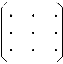
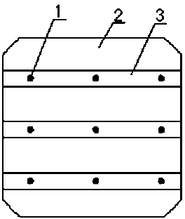
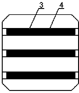
01 Multi-layer metallization stack structures
Backside metallization can be maximized through the use of multi-layer stack structures that include multiple conductive layers separated by dielectric or barrier layers. These structures allow for increased metal coverage and improved electrical conductivity while maintaining structural integrity. The stack design enables optimization of thickness and composition of each layer to achieve maximum metallization coverage on the backside of semiconductor devices.- Multi-layer metallization stack structures: Backside metallization can be maximized through the use of multi-layer stack structures that include multiple conductive layers separated by dielectric or barrier layers. These structures allow for increased metal coverage and improved electrical conductivity while maintaining proper isolation between layers. The stack design can incorporate various metal compositions and thicknesses optimized for specific electrical and thermal performance requirements.
- Advanced deposition and patterning techniques: Maximization of backside metallization layers involves employing advanced deposition methods such as physical vapor deposition, chemical vapor deposition, or electroplating to achieve uniform and thick metal layers. Precise patterning techniques including photolithography and etching processes enable the creation of fine-featured metallization patterns that maximize surface coverage while maintaining required spacing and isolation between conductive regions.
- Barrier and adhesion layer optimization: Effective backside metallization maximization requires the implementation of optimized barrier and adhesion layers between the substrate and primary metal layers. These intermediate layers prevent metal diffusion, improve adhesion, and enable the use of thicker metallization layers without delamination or reliability issues. Material selection and thickness control of these layers are critical for achieving maximum metallization coverage.
- Full-area or near-full-area backside coverage: Maximization strategies include designing metallization patterns that provide full-area or near-full-area coverage of the backside surface. This approach minimizes non-metallized regions and maximizes the effective conductive area for improved electrical performance, heat dissipation, or electromagnetic shielding. The design may incorporate grid patterns, mesh structures, or solid planes with minimal openings for process requirements.
- Thermal management and stress reduction: Backside metallization layer maximization must account for thermal management and mechanical stress considerations. Designs incorporate features such as thermal expansion matching, stress-relief patterns, and heat-spreading geometries that allow for maximum metal coverage while preventing warpage, cracking, or delamination. Material selection and layer thickness are optimized to balance maximum metallization with thermal and mechanical reliability requirements.
02 Advanced deposition techniques for uniform coverage
Maximizing backside metallization involves employing advanced deposition methods such as physical vapor deposition, chemical vapor deposition, or electroplating to achieve uniform and complete metal coverage. These techniques enable precise control over layer thickness and uniformity across the entire backside surface, minimizing voids and ensuring consistent electrical properties. Process optimization includes controlling deposition parameters to maximize metal fill and coverage density.Expand Specific Solutions03 Barrier layer integration for enhanced adhesion
The incorporation of barrier layers between the substrate and metallization layers enhances adhesion and prevents diffusion, thereby maximizing the effectiveness of backside metallization. These barrier layers can be composed of materials that provide excellent adhesion properties while preventing metal migration. The strategic placement and composition of barrier layers allows for thicker metallization layers without compromising device reliability or performance.Expand Specific Solutions04 Patterning and etching optimization
Maximizing backside metallization coverage requires optimized patterning and etching processes that minimize material loss and maximize the metal area. Advanced lithography and etching techniques enable fine-pitch patterns with high metal density while maintaining precise dimensional control. Process refinements focus on reducing undercut and improving sidewall profiles to increase the effective metallization area and enhance electrical connectivity.Expand Specific Solutions05 Thermal management through metallization design
Backside metallization can be maximized by designing metal layers that also serve thermal management functions, allowing for increased metal thickness and coverage. The metallization structure acts as a heat spreader or heat sink, enabling thicker metal layers that improve both electrical and thermal performance. Design considerations include metal composition, layer thickness, and pattern geometry to optimize heat dissipation while maximizing metallization coverage.Expand Specific Solutions
Key Players in Solar Metallization and Equipment Industry
The backside metallization technology for solar panels represents a rapidly evolving sector within the mature photovoltaic industry, currently valued at over $200 billion globally. The competitive landscape is characterized by intense innovation as manufacturers seek efficiency improvements and cost reductions. Leading solar manufacturers like Trina Solar, Jinko Solar, and Jolywood are driving commercial implementation, while research institutions including Fraunhofer-Gesellschaft and CEA are advancing fundamental metallization techniques. Equipment suppliers such as Applied Materials and Gebr. Schmid provide critical manufacturing tools, and materials companies like DuPont and Sun Chemical develop specialized conductive pastes and substrates. The technology has reached commercial maturity with companies like Maxeon Solar and REC Solar implementing advanced backside contact architectures, though continuous innovation in materials science and processing techniques maintains competitive differentiation across the value chain.
Trina Solar Co., Ltd.
Technical Solution: Trina Solar has developed advanced backside metallization technologies focusing on multi-layer contact structures for their high-efficiency solar panels. Their approach utilizes selective emitter technology combined with optimized rear contact patterns to maximize current collection while minimizing resistive losses. The company implements fine-line printing techniques with silver-aluminum paste combinations to create multiple metallization layers that enhance electrical conductivity. Their backside design incorporates localized back surface field regions with carefully engineered contact spacing to optimize carrier collection efficiency. This technology has been successfully integrated into their PERC and TOPCon cell architectures, achieving improved fill factors and overall module performance through enhanced current extraction capabilities.
Strengths: Leading market position with proven manufacturing scalability and cost-effective production processes. Weaknesses: Limited differentiation in metallization technology compared to premium competitors, facing margin pressure from commoditization.
Jinko Solar Co., Ltd.
Technical Solution: Jinko Solar has implemented advanced backside metallization strategies in their Tiger series panels, utilizing multi-busbar technology combined with optimized rear contact designs. Their approach focuses on reducing series resistance through increased metallization coverage while maintaining cost efficiency. The company employs selective laser processing to create precise contact openings, followed by multi-layer screen printing of specialized conductive pastes. Their backside metallization incorporates aluminum-silver composite materials with engineered firing profiles to achieve optimal contact formation. Jinko's technology emphasizes the balance between electrical performance and material costs, implementing smart busbar designs that maximize current collection efficiency. The metallization pattern is optimized through computational modeling to minimize power losses while ensuring reliable mechanical adhesion and long-term durability under various environmental conditions.
Strengths: Cost-effective manufacturing with high-volume production capabilities and strong global market presence. Weaknesses: Technology differentiation challenges in competitive market, with limited premium positioning compared to specialized technology providers.
Core Patents in Advanced Metallization Layer Design
Metallization method for back contact solar battery
PatentActiveCN103872181A
Innovation
- Using a combination of an insulating dielectric layer and a second metal layer, circular or point-shaped N-type metal contacts are formed on the back of the semiconductor substrate, and openings are provided on the insulating dielectric layer to reduce the metal contact area and reduce the concentration of the silver paste. consumption, and a welding electrode is formed through the second metal layer to achieve a stable connection of the components.

Method for production of wafer based solar panels
PatentActiveUS20140238463A1
Innovation
- Adapting the CSG-technology for wafer-based solar cell production by pre-processing wafers to combine cell metallization and module interconnects in a single metal process, attaching them to a transparent front glass, and patterning a metal layer to form electrical contacts and interconnections.


Environmental Impact Assessment of Metallization Processes
The environmental implications of backside metallization processes in solar panel manufacturing present significant considerations for sustainable photovoltaic production. Traditional screen printing methods utilizing silver-based pastes generate substantial material waste, with typical utilization rates ranging from 60-70%, resulting in considerable precious metal losses. The shift toward maximized backside metallization layers intensifies these environmental concerns due to increased material consumption and processing complexity.
Solvent-based metallization processes introduce volatile organic compound emissions during curing and drying stages. These emissions require sophisticated ventilation systems and thermal oxidation equipment to meet environmental regulations. The energy intensity of high-temperature firing processes, typically operating at 700-900°C, contributes significantly to the carbon footprint of solar panel production, particularly when maximizing metallization coverage areas.
Alternative metallization approaches demonstrate varying environmental profiles. Physical vapor deposition and electroplating processes eliminate solvent emissions but require substantial electrical energy inputs and generate different waste streams. Copper-based metallization systems, while reducing precious metal dependency, introduce concerns regarding metal ion contamination in wastewater streams and require specialized treatment protocols.
Water consumption represents another critical environmental factor, particularly in wet chemical processes and cleaning operations. Maximized metallization layers necessitate enhanced surface preparation and post-processing cleaning, increasing water usage by 15-25% compared to standard configurations. Wastewater treatment systems must accommodate higher concentrations of metallic contaminants and organic residues.
Life cycle assessments indicate that optimized backside metallization can improve overall environmental performance through enhanced energy conversion efficiency, offsetting manufacturing impacts within 6-12 months of operation. However, end-of-life recycling challenges emerge due to increased material complexity and bonding strength in maximized metallization structures.
Emerging green chemistry approaches, including water-based pastes and low-temperature processing techniques, offer pathways to reduce environmental impacts while maintaining performance objectives. These innovations align with circular economy principles and regulatory frameworks promoting sustainable manufacturing practices in the photovoltaic industry.
Cost-Benefit Analysis of Maximized Metallization Layers
The economic evaluation of maximized backside metallization layers in solar panels reveals a complex interplay between initial investment costs and long-term performance benefits. Manufacturing costs increase substantially when implementing additional metallization layers, primarily due to enhanced material requirements and extended processing time. Silver paste consumption rises by approximately 15-25% per additional layer, while screen printing and curing cycles extend manufacturing duration by 8-12%. Equipment utilization efficiency decreases correspondingly, impacting overall production throughput and facility capacity.
Capital expenditure analysis indicates that upgrading existing production lines to accommodate maximized metallization requires significant investment in precision screen printing equipment and enhanced curing systems. The payback period for such investments typically ranges from 18-24 months, depending on production volume and market pricing conditions. However, operational expenditure benefits emerge through reduced cell rejection rates and improved yield consistency, as enhanced metallization patterns provide better current collection uniformity.
Performance-driven revenue enhancement represents the primary economic justification for maximized metallization implementation. Field data demonstrates that optimized backside metallization can improve module efficiency by 0.3-0.8%, translating to increased power output over the system's operational lifetime. For utility-scale installations, this efficiency gain generates substantial additional revenue, with levelized cost of electricity improvements ranging from 2-5% depending on local irradiance conditions and electricity pricing structures.
Long-term financial modeling reveals that despite higher initial costs, maximized metallization layers deliver positive net present value within 3-4 years of deployment. The enhanced current collection capability reduces resistive losses, maintaining higher performance degradation rates compared to conventional designs. Additionally, improved thermal management characteristics associated with optimized metallization patterns contribute to extended module lifespan, further enhancing the overall return on investment for both manufacturers and end-users in competitive photovoltaic markets.
Unlock deeper insights with PatSnap Eureka Quick Research — get a full tech report to explore trends and direct your research. Try now!
Generate Your Research Report Instantly with AI Agent
Supercharge your innovation with PatSnap Eureka AI Agent Platform!