

How to Optimize Ferroelectric RAM Density for Edge Devices
MAY 14, 20269 MIN READ
Generate Your Research Report Instantly with AI Agent
PatSnap Eureka helps you evaluate technical feasibility & market potential.
FeRAM Density Optimization Background and Objectives
Ferroelectric Random Access Memory (FeRAM) has emerged as a critical memory technology for edge computing applications, combining the non-volatility of flash memory with the speed and endurance characteristics approaching those of SRAM. The fundamental principle relies on ferroelectric materials that can maintain polarization states without power, enabling instant-on capabilities and ultra-low power consumption essential for battery-operated edge devices.
The evolution of FeRAM technology spans over three decades, beginning with early lead zirconate titanate (PZT) based implementations in the 1990s. Initial deployments focused on low-density applications such as smart cards and RFID tags, where the technology's inherent advantages of fast write speeds and virtually unlimited endurance cycles provided clear value propositions. However, density limitations constrained broader adoption in mainstream computing applications.
Contemporary edge computing paradigms have fundamentally shifted the memory requirements landscape. Edge devices must process increasing volumes of data locally while maintaining strict power budgets and form factor constraints. Traditional memory hierarchies, dominated by volatile DRAM and slow NAND flash, create bottlenecks that limit real-time processing capabilities and increase overall system power consumption through frequent data transfers.
The primary technical objective centers on achieving FeRAM densities comparable to embedded DRAM while preserving the technology's inherent advantages. Current commercial FeRAM implementations typically achieve densities in the range of 4-8 Mb, significantly lower than the multi-gigabit requirements of modern edge applications. Scaling challenges stem from the physical properties of ferroelectric materials, manufacturing process complexities, and integration difficulties with advanced semiconductor nodes.
Key density optimization targets include developing ferroelectric materials with reduced cell sizes, implementing three-dimensional memory architectures, and advancing lithographic techniques for sub-10nm feature sizes. The integration of hafnium oxide-based ferroelectric materials represents a promising pathway, offering compatibility with standard CMOS processes and potential for aggressive scaling.
The strategic importance of FeRAM density optimization extends beyond mere capacity improvements. Higher density implementations enable new edge computing architectures where processing and storage converge, reducing data movement overhead and enabling more sophisticated AI inference capabilities at the network edge. Success in this domain could fundamentally reshape the memory landscape for IoT, autonomous systems, and distributed computing applications.
Edge Device Memory Market Demand Analysis
The edge device memory market is experiencing unprecedented growth driven by the proliferation of Internet of Things applications, autonomous vehicles, industrial automation systems, and mobile computing platforms. These devices require memory solutions that can operate efficiently under strict power constraints while maintaining high performance and reliability in diverse environmental conditions.
Current market dynamics reveal a significant shift toward non-volatile memory technologies that can bridge the gap between traditional volatile RAM and slower storage solutions. Edge devices demand memory architectures that support instant-on capabilities, reduce power consumption during idle states, and provide sufficient bandwidth for real-time data processing applications.
The automotive sector represents one of the most demanding segments, where edge devices must process sensor data, execute machine learning algorithms, and maintain critical safety functions. These applications require memory densities that can accommodate complex neural network models while operating within automotive temperature ranges and reliability standards.
Industrial IoT deployments are driving demand for memory solutions that can withstand harsh environmental conditions while supporting predictive maintenance algorithms and real-time monitoring systems. The market increasingly favors memory technologies that offer both high density and low power consumption to extend device operational lifespans in remote locations.
Mobile and wearable device markets continue to push for higher memory densities in increasingly compact form factors. These applications require memory solutions that can support advanced user interfaces, continuous health monitoring, and augmented reality features while maintaining all-day battery life.
The emergence of edge AI applications has created new requirements for memory architectures that can efficiently handle both training and inference workloads. Market demand is shifting toward memory technologies that can provide the random access patterns required for neural network operations while maintaining the density advantages necessary for storing large model parameters.
Supply chain considerations are increasingly influencing market preferences, with manufacturers seeking memory technologies that can be produced using established semiconductor fabrication processes. This trend favors solutions that can leverage existing manufacturing infrastructure while delivering the performance characteristics required for next-generation edge applications.
Current FeRAM Density Limitations and Technical Challenges
Current FeRAM technology faces significant density limitations that constrain its widespread adoption in edge computing applications. The fundamental challenge stems from the relatively large cell size required for ferroelectric capacitors compared to conventional DRAM or Flash memory cells. Traditional FeRAM cells typically require 6T2C or 2T2C configurations, where each bit demands substantial silicon real estate due to the ferroelectric capacitor structure and associated transistor circuitry.
The ferroelectric material itself presents scaling challenges that directly impact density optimization. As device dimensions shrink below 100 nanometers, ferroelectric materials like lead zirconate titanate (PZT) and strontium bismuth tantalate (SBT) exhibit degraded polarization characteristics and reduced switching reliability. This phenomenon, known as size effect, occurs because the ferroelectric domains become unstable at smaller scales, leading to decreased remnant polarization and coercive field variations.
Manufacturing process limitations further compound density challenges in FeRAM production. The high-temperature processing required for ferroelectric material deposition and crystallization, typically exceeding 600°C, creates integration difficulties with advanced CMOS processes. This thermal budget constraint forces manufacturers to use specialized fabrication sequences that limit the achievable feature sizes and increase production complexity.
Endurance degradation represents another critical technical challenge affecting FeRAM density optimization. While FeRAM offers superior endurance compared to Flash memory, repeated switching cycles gradually degrade the ferroelectric properties through domain wall pinning and charge injection effects. This degradation necessitates larger cell margins and error correction overhead, effectively reducing the usable memory density for edge device applications requiring long operational lifespans.
Cross-talk interference between adjacent cells becomes increasingly problematic as manufacturers attempt to scale FeRAM arrays to higher densities. The electric fields generated during ferroelectric switching can disturb neighboring cells, particularly in densely packed arrays. This interference requires increased cell spacing and sophisticated isolation techniques, directly limiting the achievable bit density per unit area.
Power consumption scaling presents additional challenges for edge device integration. Although individual FeRAM cells consume relatively low power, the switching currents required for ferroelectric polarization reversal increase with array size and access frequency. Edge devices operating under strict power budgets require careful optimization of refresh cycles and access patterns to maintain acceptable power consumption levels while maximizing memory density utilization.
Existing FeRAM Density Enhancement Solutions
01 Memory cell structure optimization for increased density
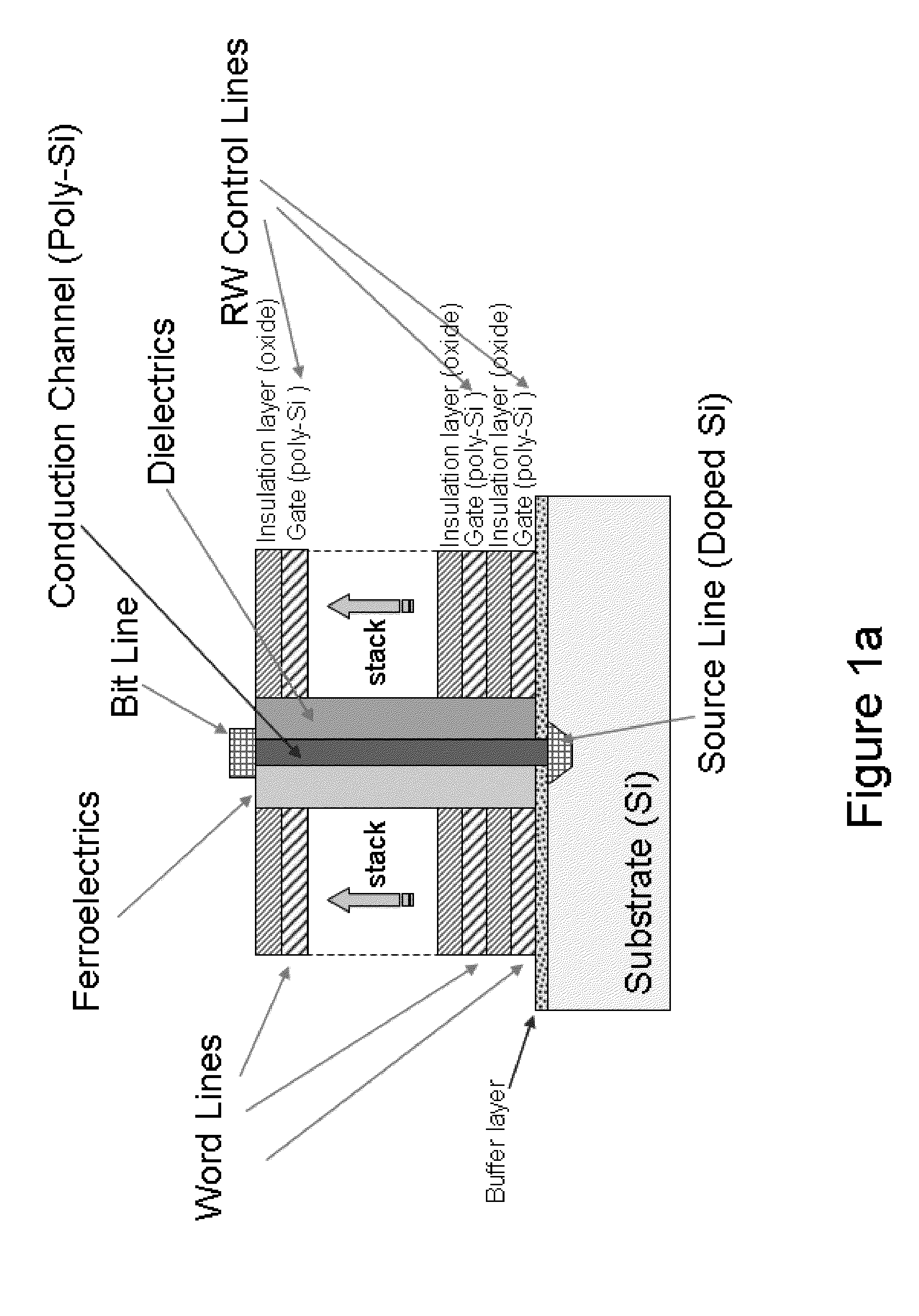
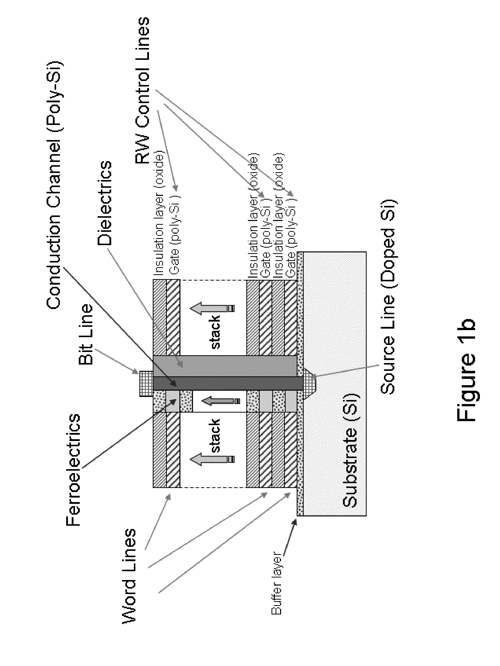
Ferroelectric RAM density can be enhanced through optimized memory cell structures that minimize the physical footprint of individual cells. This involves designing compact cell layouts, reducing parasitic capacitances, and implementing efficient addressing schemes. Advanced cell architectures allow for higher integration levels while maintaining reliable ferroelectric switching characteristics and data retention properties.- Memory cell structure optimization for increased density: Ferroelectric RAM density can be enhanced through optimized memory cell structures that minimize the physical footprint of individual cells. This includes advanced cell architectures that allow for more compact arrangements and improved space utilization. The optimization focuses on reducing cell size while maintaining reliable ferroelectric properties and data retention capabilities.
- Advanced fabrication processes for high-density arrays: Manufacturing techniques specifically designed for creating high-density ferroelectric memory arrays involve sophisticated lithography and etching processes. These methods enable the production of smaller feature sizes and tighter pitch arrangements, allowing more memory cells to be packed into the same chip area. The processes also ensure uniform ferroelectric material properties across large arrays.
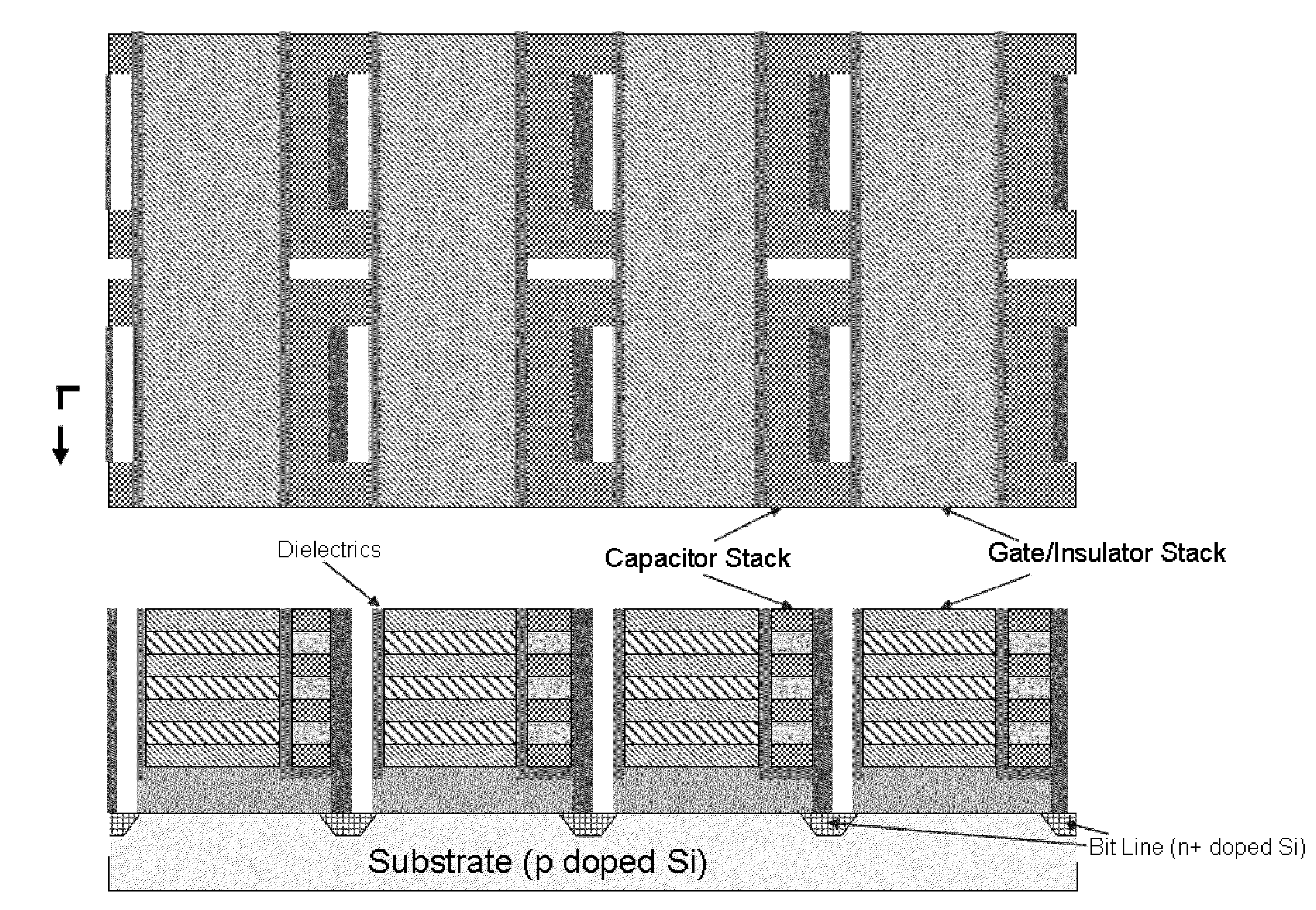
- Three-dimensional memory architectures: Three-dimensional stacking approaches significantly increase memory density by utilizing vertical space in addition to horizontal chip area. These architectures involve multiple layers of ferroelectric memory cells stacked vertically, with appropriate interconnection schemes to access individual cells. This approach can multiply the effective density compared to traditional planar designs.
- Ferroelectric material engineering for density enhancement: Development of advanced ferroelectric materials with improved properties enables higher density memory designs. These materials exhibit enhanced polarization characteristics, reduced switching voltages, and better scalability to smaller dimensions. The engineering focuses on maintaining ferroelectric behavior at reduced cell sizes while ensuring long-term stability and endurance.
- Addressing and control circuit optimization: High-density ferroelectric memory requires sophisticated addressing schemes and control circuits that can efficiently manage large numbers of memory cells. This includes optimized decoder designs, sense amplifiers, and timing control circuits that minimize overhead while maintaining fast access times. The optimization ensures that support circuitry does not significantly impact the overall memory density.
02 Three-dimensional stacking and multilayer configurations
Density improvements are achieved through vertical integration techniques that stack multiple ferroelectric memory layers in three-dimensional configurations. This approach maximizes storage capacity within a given chip area by utilizing the vertical dimension. The multilayer structures require careful consideration of inter-layer isolation, thermal management, and access circuitry to ensure proper operation of all memory levels.Expand Specific Solutions03 Advanced fabrication processes for miniaturization
High-density ferroelectric RAM relies on sophisticated manufacturing techniques that enable smaller feature sizes and tighter component spacing. These processes include advanced lithography methods, precise etching techniques, and improved material deposition controls. The fabrication innovations allow for reduced cell dimensions while preserving the ferroelectric material properties essential for memory operation.Expand Specific Solutions04 Ferroelectric material engineering and thin film optimization
Density enhancement involves developing ferroelectric materials with superior properties that enable thinner films and smaller capacitor structures. Material engineering focuses on compositions that maintain strong ferroelectric behavior at reduced dimensions, improved crystalline structures, and enhanced switching characteristics. These optimized materials allow for more compact memory cells without compromising performance or reliability.Expand Specific Solutions05 Peripheral circuit integration and area efficiency
Maximizing ferroelectric RAM density requires efficient integration of peripheral circuits including decoders, sense amplifiers, and control logic. This involves optimizing the layout of support circuitry to minimize overhead area while maintaining proper signal integrity and timing characteristics. Advanced circuit designs enable higher memory-to-logic ratios and improved overall chip utilization efficiency.Expand Specific Solutions
Major FeRAM and Edge Computing Industry Players
The ferroelectric RAM (FeRAM) density optimization market for edge devices is in an emerging growth phase, driven by increasing demand for low-power, non-volatile memory solutions in IoT and edge computing applications. The market remains relatively niche but shows significant expansion potential as edge AI applications proliferate. Technology maturity varies considerably across key players, with established memory manufacturers like Samsung Electronics, SK Hynix, and Micron Technology leading in advanced fabrication capabilities and process optimization. Foundry leaders including TSMC and GLOBALFOUNDRIES provide critical manufacturing infrastructure, while specialized companies like ROHM and Winbond Electronics focus on application-specific implementations. Research institutions such as Fudan University and Zhejiang University contribute fundamental breakthroughs in ferroelectric materials and device physics, bridging the gap between laboratory innovations and commercial viability for next-generation edge computing platforms.
Samsung Electronics Co., Ltd.
Technical Solution: Samsung has developed advanced ferroelectric memory solutions using hafnium oxide (HfO2) based ferroelectric materials integrated with their existing CMOS processes. Their approach focuses on scaling ferroelectric capacitors to sub-10nm dimensions while maintaining polarization stability through optimized crystalline structure control. The company employs atomic layer deposition (ALD) techniques to achieve precise thickness control of ferroelectric layers, enabling higher density integration. Samsung's ferroelectric RAM architecture incorporates innovative cell designs that reduce footprint by 40% compared to traditional approaches while maintaining data retention exceeding 10 years at operating temperatures up to 85°C.
Strengths: Excellent manufacturing scalability and process maturity, strong integration with existing semiconductor fabrication. Weaknesses: Higher power consumption during write operations, limited endurance cycles compared to some competing technologies.
Intel Corp.
Technical Solution: Intel's ferroelectric RAM optimization strategy centers on their proprietary 3D cross-point architecture combined with ferroelectric tunnel junctions (FTJs). They utilize ultra-thin ferroelectric films with thickness below 5nm to maximize tunneling electroresistance effects, achieving density improvements of up to 8x compared to conventional FeRAM designs. Intel's approach incorporates machine learning algorithms for wear leveling and error correction, extending device lifetime while maintaining high-speed access. Their edge-optimized variants feature adaptive voltage scaling and temperature compensation circuits, ensuring reliable operation across varying environmental conditions typical in edge computing scenarios.
Strengths: Superior read/write speed performance, excellent scalability to advanced process nodes. Weaknesses: Complex manufacturing requirements, higher initial development costs for specialized applications.
Core Patents in High-Density FeRAM Design
Three-dimensional non-volatile ferroelectric random access memory
PatentInactiveUS20160118404A1
Innovation
- Design of three-dimensional ferroelectric non-volatile memory devices with field-effect-transistors (FETs) connected in series or parallel, employing double-gate structures with ferroelectric and conventional dielectric layers for high storage density, and implementation of OR-NAND and AND-NOR logic schemes for full random access to individual memory cells.

Ferroelectric random-access memory with enhanced lifetime, density, and performance
PatentActiveUS20240087632A1
Innovation
- The implementation of ferroelectric random-access memory (FeRAM) and ferroelectric field-effect transistor (FeFET) memory structures with multiple capacitors per memory cell, reducing write-back operations and enabling multi-bit storage, independent access, and improved error recovery, while being logic-compatible with processor IC devices.


Power Efficiency Standards for Edge Memory Systems
Power efficiency standards for edge memory systems have become increasingly critical as the demand for low-power, high-performance computing at the network edge continues to grow. Current industry standards primarily focus on static power consumption metrics, with JEDEC specifications defining baseline power requirements for various memory technologies. However, these traditional standards inadequately address the dynamic power characteristics essential for ferroelectric RAM optimization in edge applications.
The IEEE 1149.10 standard provides foundational guidelines for low-power memory testing, while the ACPI specification outlines power state management protocols. These frameworks establish maximum standby power consumption limits typically ranging from 10-50 milliwatts for edge memory modules. Additionally, the Energy Star program has introduced specific criteria for edge computing devices, mandating memory subsystems achieve power efficiency ratios exceeding 85% during active operations.
Emerging standards specifically targeting edge memory systems include the Open Compute Project's Edge Hardware specifications, which define power density requirements of less than 2 watts per gigabyte for memory arrays. The ETSI Multi-access Edge Computing standards further specify that memory systems must support rapid power state transitions within 100 microseconds to optimize overall system efficiency.
Ferroelectric RAM presents unique challenges in meeting these standards due to its write power characteristics and retention mechanisms. Current power efficiency benchmarks require FeRAM implementations to demonstrate read power consumption below 50 milliwatts per gigabit while maintaining write operations within 200 milliwatts per gigabit. These specifications drive the need for advanced power management architectures and voltage scaling techniques.
Future standards development focuses on dynamic power scaling protocols that can adapt to varying workload demands in edge environments. Proposed metrics include power-per-operation measurements and thermal efficiency ratings specifically designed for non-volatile memory technologies like ferroelectric RAM, ensuring optimal performance in resource-constrained edge deployment scenarios.
Reliability Requirements for Edge FeRAM Applications
Edge computing environments impose stringent reliability requirements on FeRAM devices due to their deployment in mission-critical applications where failure tolerance is minimal. Unlike traditional computing systems with redundant backup mechanisms, edge devices often operate autonomously in remote locations, making component reliability paramount for sustained operation.
The operational temperature range represents a fundamental reliability challenge for edge FeRAM applications. These devices must maintain data integrity across extreme temperature variations, typically from -40°C to +85°C for industrial applications, and up to +125°C for automotive edge computing systems. Temperature fluctuations directly impact ferroelectric material properties, potentially causing polarization degradation and increased leakage currents that compromise data retention capabilities.
Endurance specifications for edge FeRAM applications typically demand 10^12 to 10^14 write/erase cycles, significantly higher than consumer electronics requirements. Edge devices frequently perform real-time data logging, sensor fusion, and continuous machine learning inference, generating substantial write activity. The ferroelectric material must withstand repeated polarization switching without experiencing fatigue-induced performance degradation that could lead to data corruption or device failure.
Data retention requirements extend beyond conventional memory specifications due to edge devices' extended deployment periods without maintenance access. FeRAM components must guarantee data integrity for minimum 10-year periods under operational stress conditions, including temperature cycling, humidity exposure, and electromagnetic interference. This necessitates advanced ferroelectric material engineering to minimize depolarization effects and maintain stable remnant polarization over extended timeframes.
Radiation hardness becomes critical for edge applications in aerospace, satellite communications, and nuclear facility monitoring. FeRAM devices must demonstrate immunity to single-event upsets, total ionizing dose effects, and displacement damage that could alter ferroelectric domain structures. Specialized packaging and circuit design techniques are essential to meet radiation tolerance specifications while maintaining density optimization objectives.
Power supply stability requirements are particularly stringent for battery-powered edge devices where voltage fluctuations are common. FeRAM circuits must operate reliably across wide supply voltage ranges while maintaining consistent switching characteristics. This includes implementing robust voltage regulation circuits and designing ferroelectric capacitor structures that maintain switching reliability under varying power conditions, ensuring consistent performance throughout the device's operational lifetime.
Unlock deeper insights with PatSnap Eureka Quick Research — get a full tech report to explore trends and direct your research. Try now!
Generate Your Research Report Instantly with AI Agent
Supercharge your innovation with PatSnap Eureka AI Agent Platform!