

How to Optimize High-k Dielectrics for DRAM Cell Efficiency
MAY 13, 20268 MIN READ
Generate Your Research Report Instantly with AI Agent
PatSnap Eureka helps you evaluate technical feasibility & market potential.
High-k Dielectric DRAM Evolution and Targets
The evolution of high-k dielectrics in DRAM technology represents a critical response to the fundamental scaling challenges facing semiconductor memory devices. As DRAM cell dimensions continue to shrink following Moore's Law, traditional silicon dioxide (SiO2) gate dielectrics have reached physical limitations where quantum tunneling effects severely compromise device performance and reliability. The transition from conventional SiO2 to high-k materials emerged as an essential technological shift to maintain electrostatic control while reducing leakage currents in scaled devices.
The historical development of high-k dielectrics in DRAM began in the early 2000s when industry leaders recognized that SiO2 thickness could not be reduced below 1-2 nanometers without experiencing prohibitive gate leakage. This realization drove extensive research into alternative dielectric materials with higher permittivity values, enabling thicker physical layers while maintaining equivalent electrical thickness. The progression from hafnium-based compounds to more advanced ternary and quaternary systems reflects decades of materials engineering focused on optimizing the trade-offs between dielectric constant, interface quality, and thermal stability.
Current technological targets for high-k dielectrics in DRAM applications center on achieving dielectric constants exceeding 20-25 while maintaining interface trap densities below 10^11 cm^-2eV^-1. These specifications must be met alongside stringent requirements for thermal budget compatibility with sub-20nm process nodes, where processing temperatures are increasingly constrained. The industry seeks materials that can withstand multiple high-temperature annealing cycles without significant degradation in electrical properties or unwanted interdiffusion with adjacent layers.
Performance optimization targets extend beyond basic electrical characteristics to encompass reliability metrics crucial for DRAM operation. Key objectives include achieving breakdown voltages exceeding 4-5V for projected device lifetimes, maintaining charge retention capabilities compatible with refresh rates below 32ms, and ensuring minimal threshold voltage shifts under bias-temperature stress conditions. These targets become increasingly challenging as cell capacitor areas shrink and aspect ratios increase in three-dimensional DRAM architectures.
The strategic direction for high-k dielectric development emphasizes the integration of novel materials engineering approaches with advanced deposition techniques. Future targets include the development of graded dielectric stacks that optimize interface properties while maximizing bulk dielectric performance, and the implementation of atomic layer deposition processes capable of achieving angstrom-level thickness control across high-aspect-ratio structures. These technological goals align with industry roadmaps projecting DRAM scaling continuation through the next decade.
Market Demand for Advanced DRAM Technologies
The global DRAM market continues to experience robust growth driven by the exponential increase in data generation and processing requirements across multiple sectors. Cloud computing infrastructure expansion, artificial intelligence applications, and edge computing deployments are creating unprecedented demand for high-performance memory solutions. Data centers worldwide are scaling their operations to accommodate growing workloads, necessitating memory technologies that can deliver superior speed, capacity, and energy efficiency.
Mobile device manufacturers are pushing the boundaries of performance while maintaining strict power consumption constraints. Smartphones, tablets, and wearable devices require DRAM solutions that can support advanced features like high-resolution displays, sophisticated camera systems, and real-time AI processing without compromising battery life. This creates a compelling market opportunity for optimized high-k dielectric technologies that can enhance cell efficiency and reduce power consumption.
The automotive industry represents an emerging high-growth segment for advanced DRAM technologies. Autonomous vehicles, advanced driver assistance systems, and in-vehicle infotainment platforms require reliable, high-performance memory solutions capable of operating under extreme environmental conditions. These applications demand DRAM with enhanced durability and efficiency, making high-k dielectric optimization particularly valuable.
Enterprise computing environments are experiencing a fundamental shift toward memory-intensive applications. Big data analytics, machine learning workloads, and real-time processing systems require substantial memory bandwidth and capacity. Organizations are increasingly prioritizing total cost of ownership considerations, including energy efficiency and operational reliability, when selecting memory solutions.
The Internet of Things ecosystem is generating demand for specialized DRAM solutions that can operate efficiently in resource-constrained environments. Edge computing nodes, smart sensors, and connected devices require memory technologies that balance performance requirements with power limitations. High-k dielectric optimization directly addresses these market needs by enabling more efficient DRAM cell operation.
Manufacturing cost pressures continue to intensify as semiconductor process nodes advance. Memory manufacturers are seeking technologies that can improve yield rates, reduce defect densities, and enhance overall production efficiency. Optimized high-k dielectrics offer potential solutions to these challenges while enabling continued scaling of DRAM technologies to meet growing market demand across diverse application segments.
Current High-k Dielectric Challenges in DRAM
High-k dielectric materials in DRAM cells face significant scaling challenges as device dimensions continue to shrink below 20nm technology nodes. The primary challenge lies in maintaining adequate capacitance while reducing equivalent oxide thickness (EOT) without compromising electrical performance. Traditional silicon dioxide and silicon nitride dielectrics have reached their physical limits, necessitating the adoption of high-k materials such as hafnium oxide, zirconium oxide, and aluminum oxide.
Leakage current represents one of the most critical challenges in high-k dielectric implementation. As dielectric thickness decreases to maintain capacitance density, quantum tunneling effects become increasingly prominent, leading to exponential increases in gate leakage. This phenomenon directly impacts DRAM retention time and power consumption, creating a fundamental trade-off between capacitance and leakage performance.
Interface quality between high-k dielectrics and silicon substrates poses another significant technical hurdle. Poor interface characteristics result in increased interface trap density, leading to threshold voltage instability, reduced carrier mobility, and degraded reliability. The formation of interfacial layers during deposition or subsequent thermal processing can effectively reduce the dielectric constant, negating the benefits of high-k materials.
Thermal stability issues plague many high-k dielectric candidates during DRAM processing. High-temperature annealing steps required for dopant activation and defect healing can cause crystallization of amorphous high-k films, leading to grain boundary formation and increased leakage paths. Additionally, interdiffusion between the dielectric and adjacent materials can alter the electrical properties and compromise device performance.
Process integration challenges emerge from the incompatibility of high-k materials with existing DRAM manufacturing flows. Many high-k dielectrics exhibit sensitivity to conventional wet etching chemistries, requiring development of alternative patterning techniques. The deposition uniformity across large wafer areas becomes increasingly critical as film thickness approaches atomic scales, demanding precise control of deposition parameters.
Reliability concerns include bias temperature instability, time-dependent dielectric breakdown, and charge trapping effects. High-k materials often exhibit different degradation mechanisms compared to conventional dielectrics, requiring comprehensive reliability qualification and potentially modified operating conditions to ensure acceptable device lifetime in DRAM applications.
Current High-k Dielectric Integration Solutions
01 High-k dielectric materials and compositions
Development of high dielectric constant materials that can replace traditional silicon dioxide in semiconductor applications. These materials typically include metal oxides and complex compounds that exhibit superior dielectric properties while maintaining electrical stability. The focus is on achieving higher capacitance density and improved device performance through material engineering and optimization of dielectric constant values.- High-k dielectric materials and compositions: Development of high dielectric constant materials that can replace traditional silicon dioxide in semiconductor applications. These materials exhibit superior electrical properties including higher capacitance density and reduced leakage current. The focus is on identifying and optimizing materials with dielectric constants significantly higher than conventional oxides while maintaining thermal and chemical stability.
- Deposition and fabrication methods for high-k dielectrics: Advanced processing techniques for depositing high-k dielectric layers with controlled thickness and uniformity. These methods include atomic layer deposition, chemical vapor deposition, and sputtering techniques that ensure proper interface formation and minimize defects. The processes are optimized to achieve consistent electrical properties across large substrate areas.
- Interface engineering and barrier layers: Techniques for managing the interface between high-k dielectric materials and semiconductor substrates to prevent unwanted reactions and maintain electrical performance. This includes the use of interfacial layers, surface treatments, and barrier materials that preserve the integrity of the dielectric stack while ensuring proper electrical contact and minimizing interface states.
- Device integration and performance optimization: Methods for incorporating high-k dielectrics into various semiconductor devices including transistors, capacitors, and memory cells. The focus is on optimizing device performance parameters such as switching speed, power consumption, and reliability while addressing challenges related to threshold voltage control and device scaling.
- Characterization and reliability assessment: Comprehensive testing and evaluation methods for high-k dielectric materials to assess their electrical, thermal, and mechanical properties. This includes reliability testing under various stress conditions, measurement of dielectric breakdown, and long-term stability analysis to ensure the materials meet industry standards for commercial applications.
02 Deposition and fabrication methods for high-k dielectrics
Advanced processing techniques for depositing high-k dielectric layers with controlled thickness and uniformity. These methods include atomic layer deposition, chemical vapor deposition, and sputtering processes that ensure optimal film quality and interface properties. The techniques focus on achieving precise control over film characteristics and minimizing defects during manufacturing.Expand Specific Solutions03 Interface engineering and barrier layers
Optimization of interfaces between high-k dielectric materials and semiconductor substrates to minimize leakage current and improve reliability. This involves the use of interfacial layers, surface treatments, and barrier materials that prevent unwanted reactions and maintain electrical integrity. The approach addresses compatibility issues and enhances overall device performance.Expand Specific Solutions04 Device integration and scaling applications
Implementation of high-k dielectrics in various semiconductor devices including transistors, capacitors, and memory cells. The focus is on achieving successful integration while maintaining device functionality and meeting scaling requirements. This includes addressing challenges related to threshold voltage control, mobility degradation, and process compatibility in advanced technology nodes.Expand Specific Solutions05 Performance optimization and reliability enhancement
Strategies for improving the electrical performance and long-term reliability of high-k dielectric systems. This encompasses techniques for reducing defect density, controlling charge trapping, and enhancing breakdown voltage characteristics. The approaches aim to achieve stable operation under various stress conditions and extend device lifetime while maintaining high efficiency.Expand Specific Solutions
Key High-k Material Patents and Innovations
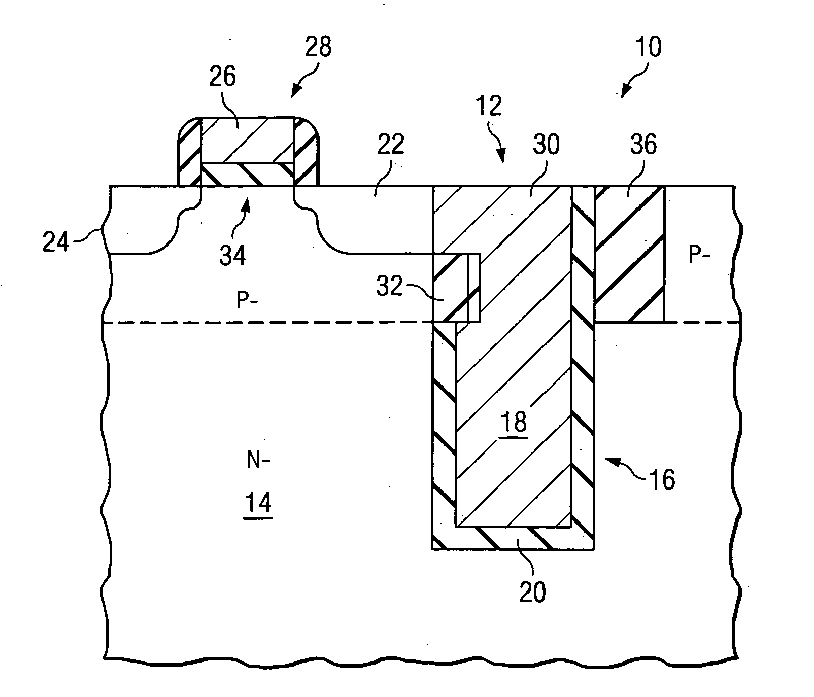
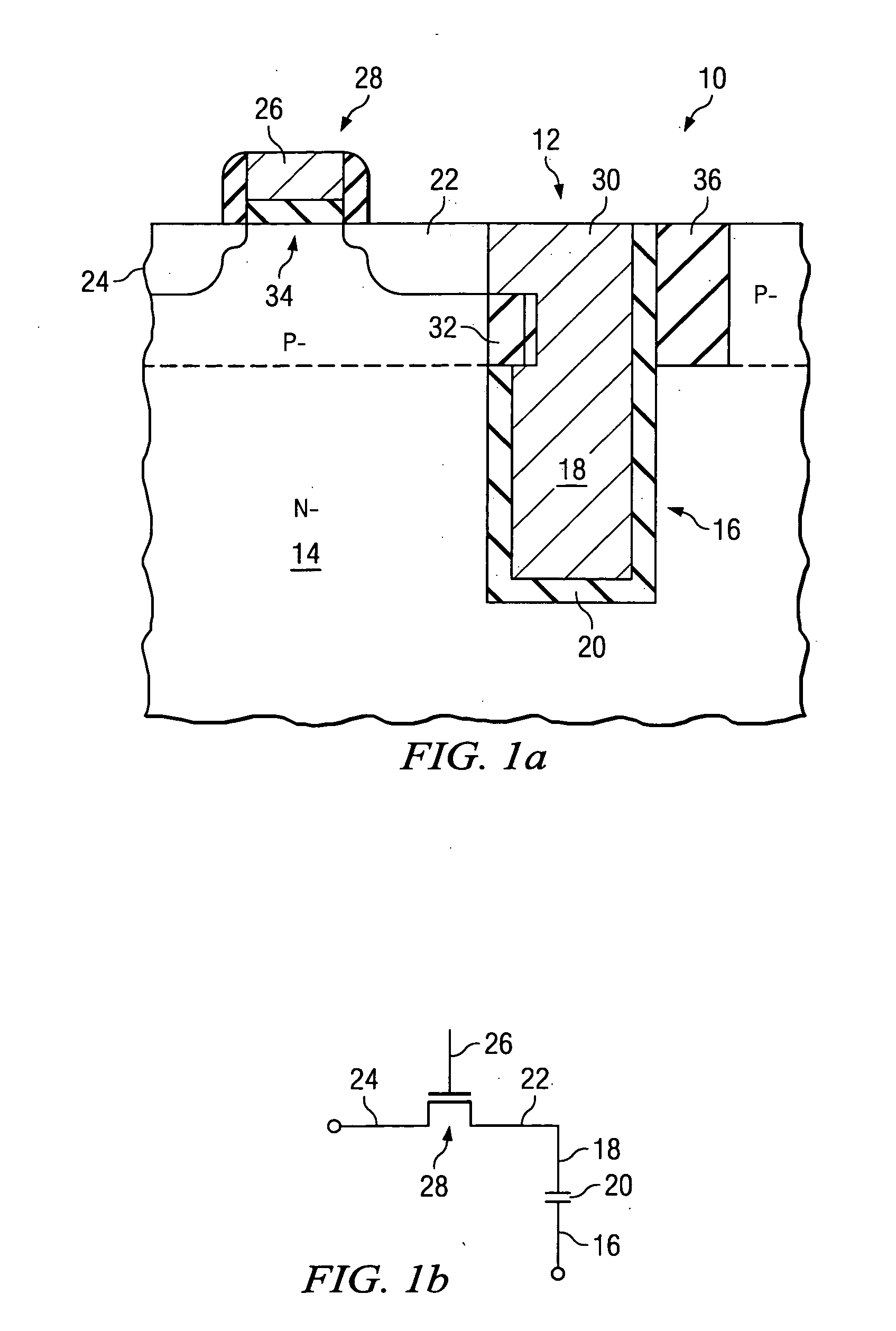
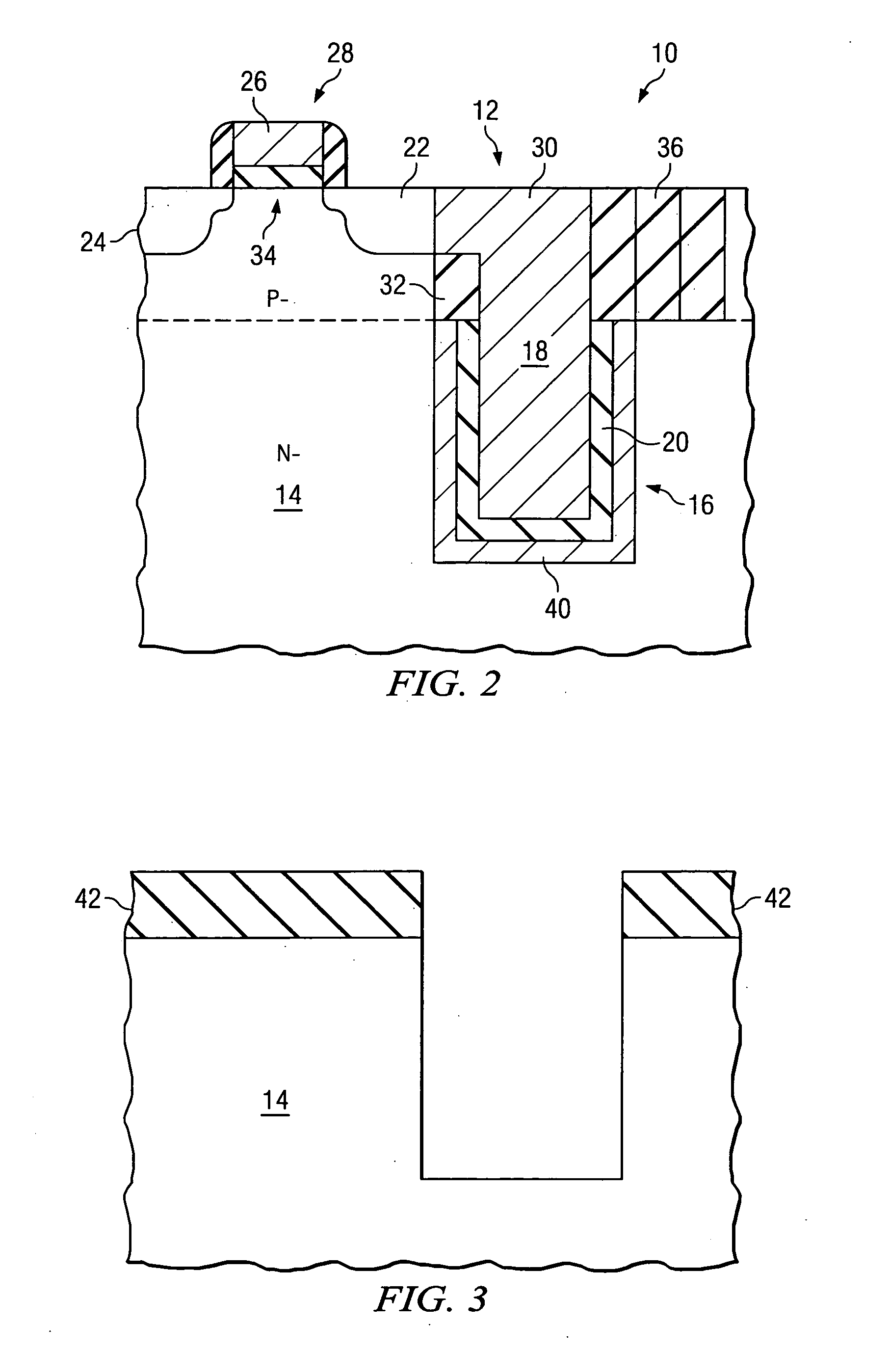
DRAM with high K dielectric storage capacitor and method of making the same
PatentInactiveUS20060151822A1
Innovation
- The development of a DRAM with a high K dielectric storage capacitor involves a metal layer adjacent to a silicon capacitor plate, a high K dielectric layer with a dielectric constant greater than 5, and the use of oxygen/nitrogen gettering layers or nanolaminate structures based on TiO2, HfO2, and Ta2O5 to enhance dielectric constants up to 35, along with the formation of conductive silicide layers to minimize interfacial contributions to EOT.

Dynamic random access memory (DRAM) cell having a buried horizontal trench capacitor by a novel fabrication method
PatentInactiveUS6218693B1
Innovation
- The method involves forming buried horizontal trench capacitors with an epitaxial layer, allowing the FET gate electrode and shallow trench isolation to be built over the capacitor, increasing capacitance without deep trenches and freeing up space for bit lines, thus reducing cell size and improving reliability and cost performance.


Semiconductor Manufacturing Standards Impact
The optimization of high-k dielectrics for DRAM cell efficiency operates within a complex framework of semiconductor manufacturing standards that significantly influence material selection, process development, and performance validation. International standards organizations such as JEDEC, SEMI, and IEEE establish critical guidelines that govern the implementation of advanced dielectric materials in memory device manufacturing.
JEDEC standards particularly impact high-k dielectric optimization through specifications for electrical performance, reliability testing, and thermal cycling requirements. These standards define acceptable leakage current thresholds, breakdown voltage specifications, and endurance criteria that high-k materials must meet. The JESD22 series standards establish environmental stress testing protocols that directly influence material composition choices and deposition process parameters for dielectric layers.
Manufacturing process standards significantly affect the integration of high-k dielectrics into DRAM production lines. SEMI equipment standards dictate chamber design requirements, gas purity specifications, and contamination control measures that are crucial for achieving consistent dielectric properties. The precision requirements for atomic layer deposition and chemical vapor deposition processes are governed by these standards, directly impacting the uniformity and quality of high-k films.
Quality control standards establish the metrology requirements for characterizing high-k dielectric properties throughout the manufacturing process. Standards for electrical testing, thickness measurement, and defect detection create benchmarks that influence both material development and process optimization strategies. These requirements often drive the selection of specific high-k materials and deposition techniques.
Emerging standards for advanced node technologies are reshaping high-k dielectric optimization approaches. New specifications for sub-10nm processes introduce stricter requirements for interface quality, thermal stability, and scalability that challenge traditional material solutions. Compliance with these evolving standards necessitates continuous innovation in dielectric material engineering and process development methodologies.
Environmental Considerations in High-k Processing
The environmental implications of high-k dielectric processing for DRAM applications present significant challenges that require comprehensive assessment and mitigation strategies. Manufacturing processes for high-k materials typically involve hazardous chemicals, including metal-organic precursors, fluorinated compounds, and various etching gases that pose risks to both human health and environmental safety. These materials often exhibit high global warming potential and require specialized handling protocols to prevent atmospheric release.
Water consumption represents a critical environmental concern in high-k dielectric fabrication. The deposition and patterning processes demand ultra-pure water for cleaning and rinsing operations, with semiconductor facilities consuming millions of gallons daily. Additionally, wastewater generated during high-k processing contains metal contaminants and organic residues that necessitate advanced treatment systems before discharge, significantly increasing operational costs and environmental footprint.
Energy consumption during high-k dielectric processing substantially exceeds that of conventional silicon dioxide fabrication. Atomic layer deposition and chemical vapor deposition techniques require elevated temperatures and extended processing times, leading to increased carbon emissions. The need for ultra-high vacuum systems and sophisticated temperature control further amplifies energy requirements, making sustainability a paramount concern for manufacturers.
Waste management challenges emerge from the complex chemical compositions used in high-k processing. Spent precursor materials, contaminated substrates, and process byproducts often contain heavy metals and persistent organic compounds that require specialized disposal methods. The limited recyclability of these materials creates long-term environmental liabilities that manufacturers must address through comprehensive waste reduction strategies.
Regulatory compliance adds another layer of complexity to environmental considerations. Stringent emissions standards for volatile organic compounds and particulate matter require continuous monitoring and control systems. International environmental regulations, including REACH and RoHS directives, mandate detailed chemical reporting and restrict the use of certain hazardous substances, influencing material selection and process design decisions.
Emerging green chemistry approaches offer promising solutions for reducing environmental impact. Alternative precursor materials with lower toxicity profiles, solvent-free processing techniques, and closed-loop chemical recovery systems represent viable pathways toward sustainable high-k dielectric manufacturing. These innovations require careful evaluation to ensure they maintain the stringent performance requirements necessary for advanced DRAM applications.
Unlock deeper insights with PatSnap Eureka Quick Research — get a full tech report to explore trends and direct your research. Try now!
Generate Your Research Report Instantly with AI Agent
Supercharge your innovation with PatSnap Eureka AI Agent Platform!