

How to Optimize Through-Glass Via Patterns for Error Reduction
APR 27, 20269 MIN READ
Generate Your Research Report Instantly with AI Agent
PatSnap Eureka helps you evaluate technical feasibility & market potential.
TGV Technology Background and Optimization Goals
Through-Glass Via (TGV) technology represents a critical advancement in three-dimensional integrated circuit packaging, enabling vertical electrical connections through glass substrates. This technology emerged from the semiconductor industry's relentless pursuit of miniaturization and performance enhancement, addressing the fundamental challenge of creating reliable interconnects in increasingly complex electronic systems. TGV structures facilitate signal transmission between different layers of integrated circuits while maintaining electrical isolation and mechanical stability.
The evolution of TGV technology stems from the limitations of traditional wire bonding and flip-chip packaging methods, which struggle to meet the demands of modern high-density applications. Glass substrates offer superior electrical properties, including low dielectric constant and excellent thermal stability, making them ideal candidates for advanced packaging solutions. However, the manufacturing process introduces inherent challenges related to via formation, metallization, and pattern optimization.
Current TGV fabrication processes involve laser drilling, chemical etching, or mechanical drilling to create microscopic holes through glass wafers, followed by metallization steps to establish conductive pathways. The precision required for these operations is extraordinary, with via diameters typically ranging from 10 to 100 micrometers and aspect ratios exceeding 10:1. Manufacturing variations, material properties, and process parameters contribute to defects that can compromise device reliability and yield.
The primary optimization goals for TGV patterns focus on minimizing electrical failures, reducing signal integrity issues, and enhancing manufacturing yield. Error reduction encompasses multiple dimensions, including via resistance variation, electrical shorts, open circuits, and signal crosstalk between adjacent vias. Pattern optimization strategies must balance electrical performance requirements with manufacturing constraints and cost considerations.
Advanced simulation tools and machine learning algorithms are increasingly employed to predict optimal via arrangements and identify potential failure modes before physical implementation. These approaches consider factors such as thermal expansion coefficients, stress distribution, and electromagnetic interference to develop robust TGV designs that maintain performance across varying operating conditions and manufacturing tolerances.
Market Demand for Advanced TGV Pattern Solutions
The semiconductor industry's relentless pursuit of miniaturization and enhanced performance has created substantial market demand for advanced Through-Glass Via (TGV) pattern solutions. As electronic devices become increasingly compact while requiring higher functionality, manufacturers face mounting pressure to develop more sophisticated packaging technologies that can accommodate dense interconnect structures without compromising reliability.
Consumer electronics manufacturers represent the largest demand segment for optimized TGV patterns, driven by the proliferation of smartphones, tablets, and wearable devices. These applications require ultra-thin form factors with exceptional electrical performance, making error-free TGV implementation critical for product success. The automotive sector has emerged as another significant growth driver, particularly with the expansion of electric vehicles and autonomous driving systems that demand robust glass-based electronic components capable of withstanding harsh environmental conditions.
The display technology market continues to fuel demand for advanced TGV solutions, especially in high-resolution OLED and micro-LED applications where precise via formation directly impacts visual quality and manufacturing yield. Touch panel manufacturers increasingly require TGV patterns with minimal defect rates to meet stringent optical and electrical specifications demanded by premium display applications.
Industrial and medical device sectors present growing opportunities for TGV pattern optimization, where reliability requirements often exceed consumer electronics standards. These applications typically involve longer product lifecycles and stricter quality control measures, creating demand for TGV solutions with proven error reduction capabilities and enhanced long-term stability.
Market research indicates that packaging substrate manufacturers are actively seeking TGV pattern solutions that can achieve higher aspect ratios while maintaining dimensional accuracy and electrical integrity. The transition toward heterogeneous integration and system-in-package architectures has intensified requirements for precise via placement and consistent electrical characteristics across large substrate areas.
Supply chain considerations have further amplified demand for optimized TGV patterns, as manufacturers seek to reduce production waste and improve overall equipment effectiveness. Companies are increasingly prioritizing solutions that demonstrate measurable improvements in defect reduction and process repeatability, recognizing that TGV pattern optimization directly correlates with manufacturing cost reduction and competitive advantage in rapidly evolving technology markets.
Current TGV Pattern Challenges and Error Sources
Through-Glass Via (TGV) technology faces significant manufacturing challenges that directly impact yield rates and device reliability in advanced semiconductor packaging. The primary error sources stem from the complex multi-step fabrication process, where each stage introduces potential defects that can compromise the final product performance.
Glass substrate preparation represents the initial challenge, where surface roughness variations and contamination can create non-uniform conditions for subsequent processing steps. Micro-cracks and stress concentrations in the glass material often propagate during thermal cycling, leading to via failure and electrical discontinuity. The inherent brittleness of glass substrates makes them particularly susceptible to mechanical damage during handling and processing.
Via drilling precision constitutes another critical challenge, particularly when achieving high aspect ratios required for miniaturized packages. Laser drilling processes frequently generate heat-affected zones that alter the glass structure around via openings, creating stress concentrations and potential crack initiation sites. Dimensional variations in via diameter and taper angle directly affect subsequent metallization quality and electrical performance.
Metallization uniformity presents substantial difficulties in TGV manufacturing. Achieving consistent copper deposition across varying via geometries while maintaining adequate step coverage remains problematic. Poor adhesion between metal layers and glass surfaces leads to delamination, while non-uniform current distribution during electroplating creates thickness variations that impact electrical characteristics and reliability.
Thermal management challenges arise from the coefficient of thermal expansion mismatch between glass substrates and metallic interconnects. This mismatch generates mechanical stress during temperature cycling, causing via cracking, metal fatigue, and eventual electrical failure. The stress concentration at via corners and edges particularly accelerates failure mechanisms.
Pattern density variations across the substrate create additional complications. High-density via regions experience different thermal and mechanical behavior compared to sparse areas, leading to warpage and stress distribution non-uniformities. This variation affects the overall package reliability and creates challenges in maintaining consistent electrical performance across the entire device.
Contamination control throughout the fabrication process remains a persistent challenge. Organic residues, metallic particles, and ionic contamination can significantly impact via formation quality and long-term reliability. These contaminants often become trapped during the multi-layer build-up process, creating potential failure sites that manifest during operational stress conditions.
Existing TGV Pattern Optimization Approaches
01 Optical correction and compensation methods
Methods for correcting optical distortions and pattern errors in through-glass via formation by implementing compensation algorithms and optical correction techniques. These approaches focus on adjusting exposure parameters and using advanced optical systems to minimize pattern deviations and improve via formation accuracy.- Optical proximity correction and pattern compensation techniques: Advanced computational methods are employed to predict and compensate for optical distortions that occur during the lithographic patterning of through-glass vias. These techniques involve pre-distorting mask patterns to counteract known systematic errors, using sophisticated algorithms to model light diffraction effects and adjust feature geometries accordingly. The compensation methods help achieve more accurate via positioning and dimensional control.
- Advanced metrology and measurement systems for via characterization: Sophisticated measurement and inspection systems are utilized to detect, quantify, and analyze pattern errors in through-glass via structures. These systems employ high-resolution imaging, interferometry, and automated defect detection algorithms to provide precise feedback on via dimensions, positioning accuracy, and profile characteristics. The measurement data enables real-time process adjustments and quality control.
- Process parameter optimization and control methods: Systematic approaches to optimize and control critical process parameters during through-glass via formation to minimize pattern errors. This includes precise control of exposure conditions, development parameters, etching processes, and environmental factors. Statistical process control methods and feedback systems are implemented to maintain consistent via quality and reduce variability across the substrate.
- Multi-step patterning and alignment strategies: Implementation of multi-layer patterning approaches with enhanced alignment techniques to achieve precise via placement and reduce cumulative errors. These methods involve sequential patterning steps with intermediate alignment verification, advanced overlay control systems, and compensation for substrate distortion effects. The strategies help maintain accuracy across multiple processing layers.
- Material and substrate engineering for improved pattern fidelity: Development of specialized materials, coatings, and substrate treatments that enhance pattern transfer accuracy and reduce error propagation during through-glass via formation. This includes anti-reflective coatings, stress-reduction layers, and surface treatments that improve adhesion and dimensional stability. The engineered materials help maintain pattern integrity throughout the fabrication process.
02 Process parameter optimization and control
Techniques for optimizing manufacturing process parameters to reduce errors in through-glass via patterns. This includes controlling temperature, pressure, timing, and other critical process variables during via formation to achieve better dimensional accuracy and reduce pattern variations.Expand Specific Solutions03 Advanced lithography and patterning techniques
Implementation of sophisticated lithography methods and patterning strategies to enhance the precision of through-glass via formation. These techniques involve improved mask designs, exposure methods, and pattern transfer processes to minimize errors and achieve better pattern fidelity.Expand Specific Solutions04 Material and substrate treatment methods
Approaches focusing on glass substrate preparation and material treatment to reduce pattern errors during via formation. These methods involve surface treatments, material selection, and substrate conditioning techniques that improve the consistency and accuracy of via patterns.Expand Specific Solutions05 Measurement and feedback control systems
Implementation of real-time measurement systems and feedback control mechanisms to monitor and correct pattern errors during through-glass via formation. These systems use advanced metrology and control algorithms to detect deviations and make real-time adjustments to maintain pattern accuracy.Expand Specific Solutions
Key Players in TGV and Glass Processing Industry
The through-glass via (TGV) optimization technology is in a rapidly evolving growth stage, driven by increasing demand for advanced packaging solutions in consumer electronics and automotive applications. The market demonstrates significant expansion potential as 3D integration becomes critical for miniaturization and performance enhancement. Technology maturity varies considerably across key players, with established semiconductor manufacturers like GLOBALFOUNDRIES, SMIC, and Shanghai Huali Microelectronics leading in foundry capabilities, while specialized companies such as Shenzhen Guihua Intelligent Technology focus on ultra-fast laser processing equipment for TGV manufacturing. Traditional technology giants including IBM, Canon, and Sony contribute advanced materials and precision manufacturing expertise. The competitive landscape shows a mix of mature foundry operations and emerging specialized solution providers, indicating the technology is transitioning from early development to commercial deployment phases, with significant opportunities for error reduction optimization through improved pattern design and manufacturing processes.
GLOBALFOUNDRIES, Inc.
Technical Solution: GLOBALFOUNDRIES has developed advanced through-glass via (TGV) fabrication processes for 3D integration applications. Their approach focuses on optimizing via diameter, pitch, and aspect ratio to minimize electrical parasitic effects and mechanical stress. The company employs deep reactive ion etching (DRIE) techniques combined with precise metallization processes to achieve high-quality TGV structures. They utilize advanced process control methodologies including real-time monitoring of etch profiles and sidewall roughness to reduce pattern-dependent variations. Their TGV optimization includes careful selection of glass substrates with matched thermal expansion coefficients and implementation of stress-relief structures around via arrays to prevent cracking and delamination during thermal cycling.
Strengths: Extensive foundry experience and advanced process control capabilities. Weaknesses: Limited to specific glass substrate types and higher manufacturing costs.
International Business Machines Corp.
Technical Solution: IBM has pioneered TGV pattern optimization through computational modeling and machine learning approaches. Their methodology involves using finite element analysis to predict stress distributions and electrical performance variations across different via geometries and arrangements. IBM's approach includes developing proprietary algorithms that optimize via placement patterns to minimize crosstalk and signal integrity issues while maintaining mechanical reliability. They have implemented advanced metrology techniques using X-ray tomography and scanning electron microscopy to characterize TGV quality and correlate manufacturing parameters with electrical performance. Their optimization framework considers both individual via characteristics and array-level interactions to achieve optimal overall system performance.
Strengths: Strong R&D capabilities and advanced simulation tools for pattern optimization. Weaknesses: Solutions may be complex to implement in high-volume manufacturing environments.
Core Innovations in TGV Error Reduction Techniques
Through glass via (TGV) with modulated profile for core stress reduction
PatentPendingUS20250113434A1
Innovation
- Implementing via geometries with rounded corners, non-uniform thickness liners, multi-segment sidewalls, and dual-layer liner structures to reduce stress concentrations, using a combination of laser-assisted etching and ultrafast laser inscription processes for precise corner rounding and stress absorption.


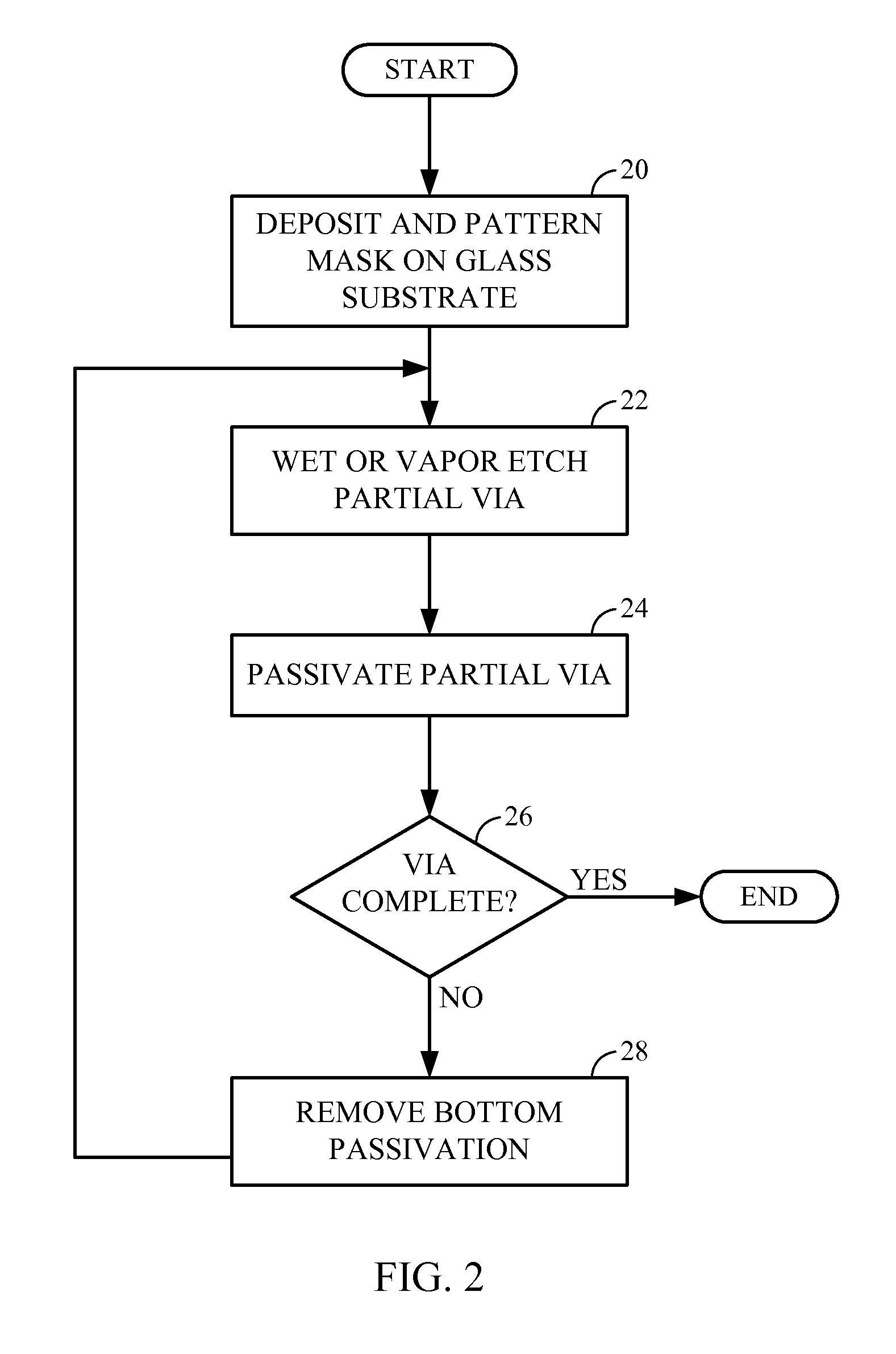
Through Glass Via Manufacturing Process
PatentInactiveUS20110229687A1
Innovation
- A process involving patterning a hard mask on a glass substrate, followed by non-plasma etching with oxide etch chemicals and passivation, repeated until a through glass via is completed, allowing for efficient creation of small pitch, vertical vias with high aspect ratios.

Manufacturing Standards for TGV Quality Control
Manufacturing standards for TGV quality control represent a critical framework that ensures consistent production outcomes and minimizes defect rates in through-glass via fabrication. These standards encompass dimensional tolerances, material specifications, and process parameters that directly influence the reliability of TGV patterns. Industry-leading manufacturers have established comprehensive quality metrics that address via diameter consistency, sidewall smoothness, and copper fill integrity as primary indicators of manufacturing excellence.
The dimensional control standards typically specify via diameter tolerances within ±2-3 micrometers for high-density applications, with aspect ratio limitations ranging from 5:1 to 10:1 depending on glass thickness and via diameter. Surface roughness parameters are maintained below 50 nanometers Ra to ensure optimal metallization adhesion and electrical performance. These specifications are enforced through statistical process control methodologies that monitor real-time production data and trigger corrective actions when parameters drift beyond acceptable limits.
Material quality standards focus on glass substrate properties, including thermal expansion coefficients, chemical composition uniformity, and stress distribution characteristics. Copper seed layer thickness uniformity is maintained within ±10% variation across the substrate surface, while electroplating bath chemistry is controlled to ensure consistent deposition rates and grain structure formation. These material standards are validated through incoming inspection protocols and periodic qualification testing of supplier materials.
Process control standards establish critical parameter windows for laser drilling, chemical etching, and metallization processes. Laser pulse energy, repetition rate, and beam positioning accuracy are monitored continuously to maintain consistent via formation characteristics. Chemical etching bath concentrations, temperature control, and agitation parameters are standardized to ensure uniform sidewall profiles and minimal taper variation across production lots.
Quality assurance protocols incorporate both in-line monitoring and final inspection procedures. Automated optical inspection systems verify via geometry and detect potential defects such as incomplete drilling, sidewall damage, or contamination. Electrical testing validates continuity, resistance values, and isolation characteristics according to predetermined acceptance criteria. Cross-sectional analysis and reliability testing provide additional verification of manufacturing quality and long-term performance expectations.
Cost-Performance Trade-offs in TGV Optimization
The optimization of Through-Glass Via (TGV) patterns presents a complex landscape of cost-performance trade-offs that significantly impact manufacturing decisions and product viability. Understanding these trade-offs is crucial for developing economically sustainable TGV solutions while maintaining acceptable performance standards.
Manufacturing cost considerations represent the primary economic constraint in TGV optimization. Advanced lithography processes required for high-precision via patterns incur substantial equipment and operational expenses. The relationship between via density and manufacturing yield creates a direct cost impact, as higher density patterns typically result in lower yields and increased production costs. Process complexity escalates with tighter design rules, requiring more sophisticated equipment and longer processing times.
Performance benefits must be carefully weighed against incremental cost increases. Optimized TGV patterns can deliver significant improvements in signal integrity, reduced crosstalk, and enhanced thermal management. However, achieving these performance gains often requires advanced materials, precise dimensional control, and sophisticated process monitoring, all contributing to higher manufacturing costs.
The economic threshold for TGV optimization varies significantly across application domains. High-performance computing and telecommunications applications can justify premium costs for superior electrical performance, while consumer electronics applications demand more cost-sensitive approaches. This market segmentation drives different optimization strategies and acceptable cost-performance ratios.
Design complexity introduces additional cost factors through increased development time and validation requirements. Complex via patterns necessitate extensive electromagnetic simulation, thermal analysis, and reliability testing, extending product development cycles and increasing engineering costs. The trade-off between design sophistication and time-to-market becomes particularly critical in competitive markets.
Yield optimization strategies play a pivotal role in managing cost-performance trade-offs. Statistical process control, adaptive manufacturing techniques, and design-for-manufacturability approaches can help maintain acceptable yields while pursuing aggressive performance targets. The investment in yield enhancement technologies must be balanced against the expected performance improvements and market requirements.
Long-term economic considerations include scalability and technology roadmap alignment. TGV optimization strategies must account for future manufacturing capabilities, material cost trends, and evolving performance requirements to ensure sustainable competitive positioning.
Unlock deeper insights with PatSnap Eureka Quick Research — get a full tech report to explore trends and direct your research. Try now!
Generate Your Research Report Instantly with AI Agent
Supercharge your innovation with PatSnap Eureka AI Agent Platform!