

How to Optimize UV Curing in Wafer Reconstitution Processes
APR 21, 20269 MIN READ
Generate Your Research Report Instantly with AI Agent
PatSnap Eureka helps you evaluate technical feasibility & market potential.
UV Curing Wafer Reconstitution Background and Objectives
Wafer reconstitution has emerged as a critical process in advanced semiconductor packaging, particularly for applications requiring ultra-thin wafers and complex multi-chip assemblies. This process involves temporarily bonding processed wafer pieces or dies onto a carrier substrate to enable further processing steps such as backside thinning, redistribution layer formation, and final packaging operations. The temporary bonding approach allows manufacturers to handle fragile thin wafers safely while maintaining precise alignment and dimensional stability throughout subsequent manufacturing stages.
UV curing technology plays a pivotal role in wafer reconstitution by providing controlled polymerization of adhesive materials used for temporary bonding. The UV curing process offers significant advantages over thermal curing methods, including reduced processing temperatures, faster cure times, and improved dimensional control. However, achieving optimal UV curing performance requires careful consideration of multiple parameters including light intensity distribution, wavelength selection, exposure duration, and thermal management during the curing process.
Current industry trends indicate increasing demand for more sophisticated wafer reconstitution processes driven by the proliferation of advanced packaging technologies such as 2.5D and 3D integration, fan-out wafer-level packaging, and system-in-package solutions. These applications require extremely precise control over adhesive properties, including adhesion strength, thermal stability, and debonding characteristics, all of which are directly influenced by UV curing optimization.
The primary technical objectives for optimizing UV curing in wafer reconstitution processes encompass several key areas. Achieving uniform cure depth and adhesive cross-linking across the entire wafer surface represents a fundamental requirement, as non-uniform curing can lead to localized stress concentrations, warpage, and potential device damage during subsequent processing steps.
Minimizing thermal effects during UV exposure constitutes another critical objective, as excessive heat generation can cause wafer warpage, adhesive degradation, or thermal stress in sensitive device structures. Advanced UV curing systems must balance sufficient photon energy delivery with effective thermal management to maintain process temperatures within acceptable limits.
Establishing precise control over adhesive mechanical properties through optimized UV exposure parameters enables fine-tuning of bond strength for specific application requirements. This includes achieving adequate adhesion for process stability while ensuring clean, residue-free debonding when temporary bonding is no longer needed.
Furthermore, developing scalable UV curing processes that maintain consistent performance across different wafer sizes, from 200mm to 300mm and beyond, represents an essential objective for high-volume manufacturing implementation. Process robustness and repeatability across multiple production tools and facilities remain paramount for successful technology deployment.
Market Demand for Advanced Wafer Reconstitution Solutions
The semiconductor industry's relentless pursuit of miniaturization and performance enhancement has created substantial demand for advanced wafer reconstitution solutions, particularly those incorporating optimized UV curing processes. As device geometries continue to shrink and packaging complexity increases, traditional wafer-level processing methods face significant limitations in handling ultra-thin dies and achieving the precision required for next-generation applications.
The proliferation of advanced packaging technologies, including fan-out wafer-level packaging, system-in-package solutions, and heterogeneous integration approaches, has fundamentally transformed market requirements. These applications demand reconstitution processes capable of maintaining dimensional stability, minimizing warpage, and ensuring uniform material properties across reconstructed wafers. UV curing optimization has emerged as a critical enabler for meeting these stringent specifications.
Mobile device manufacturers and automotive electronics suppliers represent primary demand drivers, as both sectors require increasingly sophisticated packaging solutions to accommodate multiple functionalities within constrained form factors. The automotive industry's transition toward electric vehicles and autonomous driving systems has particularly intensified requirements for reliable, high-performance semiconductor packages that can withstand harsh operating environments.
Data center and high-performance computing applications constitute another significant demand segment, where thermal management and electrical performance optimization necessitate advanced reconstitution techniques. The growing adoption of artificial intelligence and machine learning workloads has accelerated demand for specialized packaging solutions that can efficiently integrate diverse chip architectures while maintaining signal integrity.
Emerging applications in Internet of Things devices, wearable electronics, and medical implants further expand market opportunities for optimized wafer reconstitution processes. These applications often require unique form factors and specialized material properties that conventional processing methods cannot adequately address.
The market landscape reflects increasing customer sophistication, with end users demanding not only improved process capabilities but also enhanced process control, repeatability, and cost-effectiveness. This evolution has created opportunities for solution providers who can demonstrate measurable improvements in UV curing efficiency, material utilization, and overall process yield while reducing cycle times and operational complexity.
Current UV Curing Challenges in Wafer Processing
UV curing in wafer reconstitution processes faces significant technical challenges that directly impact manufacturing efficiency and product quality. The primary obstacle lies in achieving uniform light distribution across the entire wafer surface, particularly for large-diameter wafers exceeding 200mm. Non-uniform irradiance creates localized variations in polymer crosslinking density, leading to mechanical stress concentrations and potential delamination issues at die interfaces.
Temperature management represents another critical challenge during UV exposure. The exothermic nature of photopolymerization reactions generates substantial heat, causing thermal gradients that can induce wafer warpage and dimensional instability. This thermal buildup is particularly problematic in thick reconstitution layers where heat dissipation is limited, often resulting in incomplete curing in interior regions while surface layers experience overcuring.
Oxygen inhibition poses a persistent challenge in UV curing systems. Atmospheric oxygen interferes with free radical polymerization mechanisms, creating a tacky, uncured surface layer that compromises adhesion properties. This phenomenon is especially pronounced in open-air curing environments and requires sophisticated inert gas purging systems or specialized photoinitiator formulations to mitigate.
The complex geometry of reconstituted wafers introduces shadowing effects that prevent uniform UV penetration. Varying die thicknesses and irregular topographies create optical barriers, resulting in undercured regions that exhibit poor mechanical properties and reduced reliability. These geometric constraints are further complicated by the need to cure around delicate wire bonds and sensitive electronic components.
Process control and monitoring present additional challenges due to the rapid kinetics of UV curing reactions. Real-time assessment of cure progression is difficult, often relying on indirect measurements that may not accurately reflect the actual crosslinking state throughout the reconstitution layer. This limitation makes it challenging to optimize exposure parameters and ensure consistent quality across production batches.
Material compatibility issues arise when integrating UV-curable systems with existing semiconductor materials and processes. Many reconstitution materials exhibit limited UV transparency or contain additives that interfere with photoinitiator efficiency, necessitating careful formulation optimization to achieve adequate cure depth while maintaining material performance specifications.
Existing UV Curing Solutions for Wafer Reconstitution
01 UV light source configuration and intensity control
Optimization of UV curing processes through control of light source parameters including wavelength selection, intensity adjustment, and exposure time management. This involves configuring UV lamps or LED arrays to deliver optimal energy levels for specific curing applications. Advanced systems may incorporate multiple light sources with different wavelengths or adjustable intensity settings to achieve uniform curing across various substrate materials and coating thicknesses.- UV light source configuration and intensity control: Optimization of UV curing processes through control of light source parameters including wavelength selection, intensity adjustment, and exposure time management. This involves using specific UV lamp configurations, LED arrays, or mercury vapor lamps with optimized power output and spectral distribution to achieve uniform curing. Advanced systems may incorporate real-time monitoring and feedback mechanisms to maintain consistent curing quality across different substrate materials and coating thicknesses.
- UV curing equipment design and apparatus structure: Development of specialized UV curing equipment with optimized chamber designs, reflector systems, and conveyor mechanisms to enhance curing efficiency. This includes innovations in equipment layout, cooling systems for temperature management, and modular designs that allow for flexible integration into production lines. The apparatus may feature adjustable positioning systems and multiple curing stages to accommodate various product geometries and production requirements.
- UV-curable composition formulation: Optimization of photopolymerizable compositions including selection of photoinitiators, oligomers, monomers, and additives to improve curing speed and final product properties. The formulations are designed to achieve rapid polymerization under UV exposure while maintaining desired characteristics such as adhesion, flexibility, hardness, and chemical resistance. Special attention is given to balancing reactivity with stability and controlling shrinkage during the curing process.
- Process parameter control and monitoring systems: Implementation of advanced control systems for monitoring and adjusting UV curing process parameters in real-time. This includes sensors for measuring UV intensity, temperature, cure depth, and conversion rates, coupled with automated feedback loops that optimize curing conditions dynamically. The systems may incorporate data analytics and machine learning algorithms to predict optimal settings based on material properties and environmental conditions.
- Application-specific UV curing methods: Specialized UV curing techniques tailored for specific applications such as coatings, adhesives, inks, or 3D printing materials. These methods address unique challenges in different industries by optimizing cure profiles, substrate preparation, and post-cure treatments. Innovations include selective curing for multi-layer structures, gradient curing for stress management, and hybrid curing systems that combine UV with thermal or other energy sources to achieve superior results.
02 UV curing equipment design and apparatus structure
Development of specialized UV curing equipment with optimized structural designs including reflector configurations, cooling systems, and conveyor mechanisms. These apparatus improvements focus on enhancing curing efficiency through better light distribution, temperature management, and material handling. Equipment designs may incorporate features such as adjustable curing chambers, automated positioning systems, and integrated monitoring sensors to ensure consistent curing results.Expand Specific Solutions03 UV curable composition formulation
Optimization of photopolymerizable compositions including selection of photoinitiators, oligomers, monomers, and additives to enhance curing speed and final product properties. Formulation strategies focus on achieving rapid polymerization under UV exposure while maintaining desired viscosity, adhesion, and mechanical characteristics. Advanced compositions may include synergistic combinations of multiple photoinitiators or specialized additives to improve cure depth and surface finish.Expand Specific Solutions04 Process control and monitoring systems
Implementation of real-time monitoring and feedback control systems to optimize UV curing processes. These systems utilize sensors to measure parameters such as UV intensity, temperature, cure degree, and substrate position, enabling dynamic adjustment of curing conditions. Advanced control algorithms may incorporate machine learning or adaptive control strategies to compensate for variations in material properties or environmental conditions, ensuring consistent curing quality across production runs.Expand Specific Solutions05 Application-specific UV curing methods
Specialized UV curing techniques tailored for specific applications such as coatings, adhesives, inks, or three-dimensional printing. These methods address unique challenges associated with different substrates, geometries, or performance requirements. Optimization strategies may include multi-stage curing protocols, selective area curing, or combination with other processing techniques to achieve desired product characteristics while maximizing throughput and energy efficiency.Expand Specific Solutions
Key Players in UV Curing and Wafer Processing Industry
The UV curing optimization in wafer reconstitution processes represents a mature yet evolving technology segment within the advanced semiconductor packaging industry. The market demonstrates significant growth potential, driven by increasing demand for heterogeneous integration and advanced packaging solutions. Key players span the entire value chain, from equipment manufacturers like Tokyo Electron, Applied Materials, and Lam Research providing sophisticated processing systems, to material suppliers such as DuPont, Shin-Etsu Chemical, and Sekisui Chemical offering specialized UV-curable polymers and adhesives. Major foundries including TSMC and integrated device manufacturers like Sony Group drive technology requirements, while precision equipment specialists such as DISCO and Tokyo Seimitsu contribute critical dicing and measurement capabilities. The technology maturity varies across applications, with established UV curing processes being refined for next-generation packaging architectures, indicating a competitive landscape characterized by both technological sophistication and continuous innovation demands.
Taiwan Semiconductor Manufacturing Co., Ltd.
Technical Solution: TSMC has developed proprietary UV curing optimization techniques specifically tailored for advanced packaging applications in wafer reconstitution. Their approach emphasizes precise control of UV dose distribution and curing atmosphere to minimize warpage and stress in reconstituted wafers. The company has implemented advanced modeling and simulation tools to predict optimal curing parameters based on wafer geometry, material properties, and thermal constraints. Their process includes multi-step UV exposure sequences with controlled cooling phases to manage thermal gradients and prevent delamination. TSMC's methodology also incorporates in-line metrology systems that monitor wafer flatness and adhesion quality throughout the curing process, enabling real-time process adjustments to maintain yield and quality standards.
Strengths: Deep process expertise and proven high-volume manufacturing capabilities with excellent yield control. Weaknesses: Proprietary solutions may have limited applicability outside TSMC's specific process flows and equipment configurations.
DISCO Corp.
Technical Solution: DISCO has developed UV curing optimization solutions that complement their wafer dicing and grinding equipment for reconstitution processes. Their technology focuses on post-processing UV curing applications where precise control of adhesive properties is critical for subsequent handling and assembly operations. The company's approach includes specialized UV exposure systems with adjustable wavelength selection capabilities, allowing optimization for different photopolymer chemistries used in wafer reconstitution. Their systems feature advanced substrate positioning mechanisms that ensure consistent gap spacing and alignment during UV exposure, critical for achieving uniform curing results. DISCO's solutions also incorporate contamination control measures and clean room compatibility features essential for semiconductor manufacturing environments.
Strengths: Strong integration with wafer processing workflows and excellent contamination control capabilities. Weaknesses: Limited to specific applications in wafer processing sequence and requires coordination with other processing equipment for optimal results.
Core UV Curing Patents and Technical Innovations
Single-chamber sequential curing of semiconductor wafers
PatentInactiveUS8137465B1
Innovation
- The development of a multi-chamber sequential curing apparatus with independent control of wafer temperature and UV intensity, using multiple UV light sources for concurrent curing of multiple wafers, and the use of 'cold mirrors' to decouple IR radiation from UV exposure, ensuring uniformity and increased throughput.
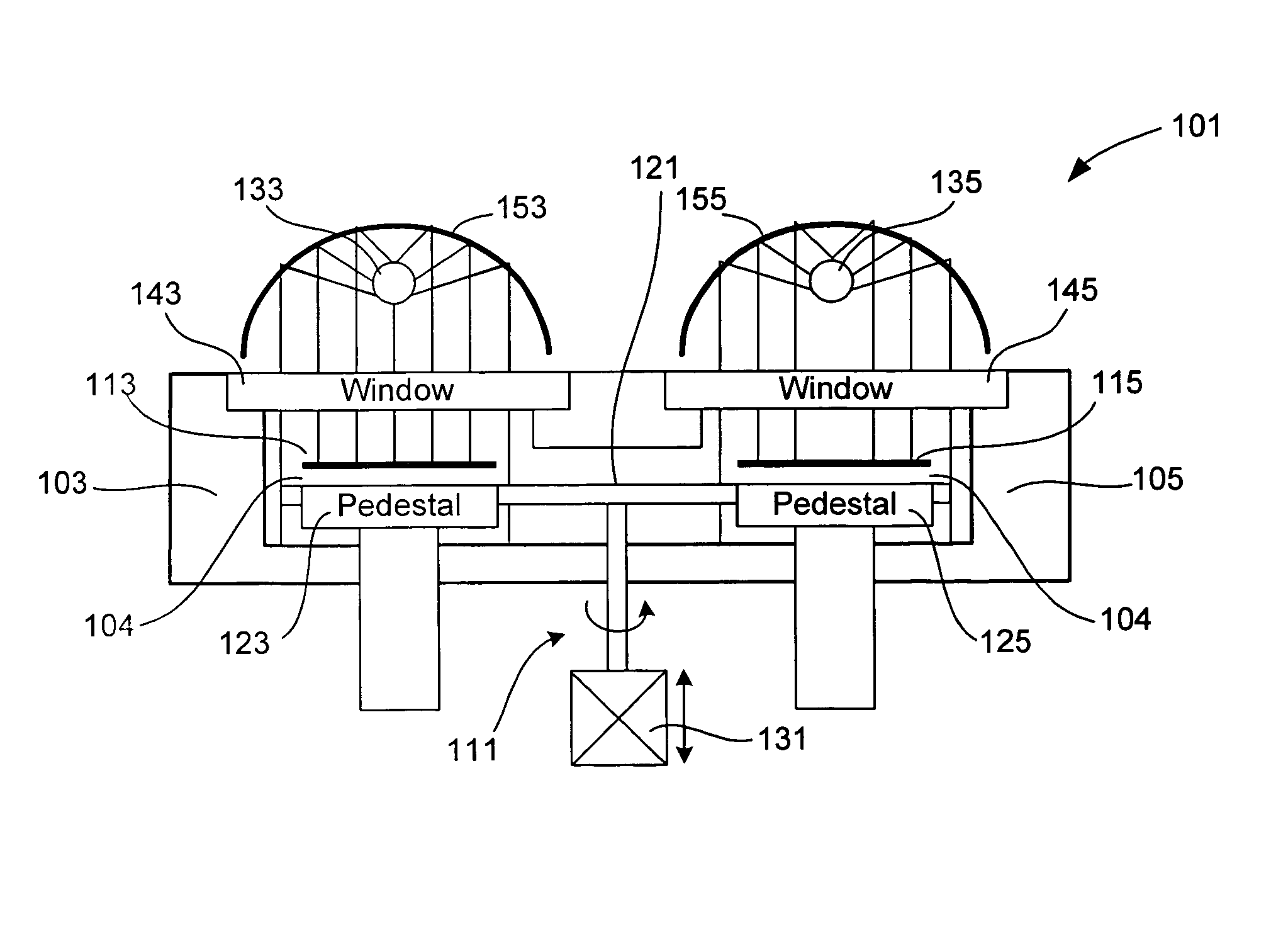
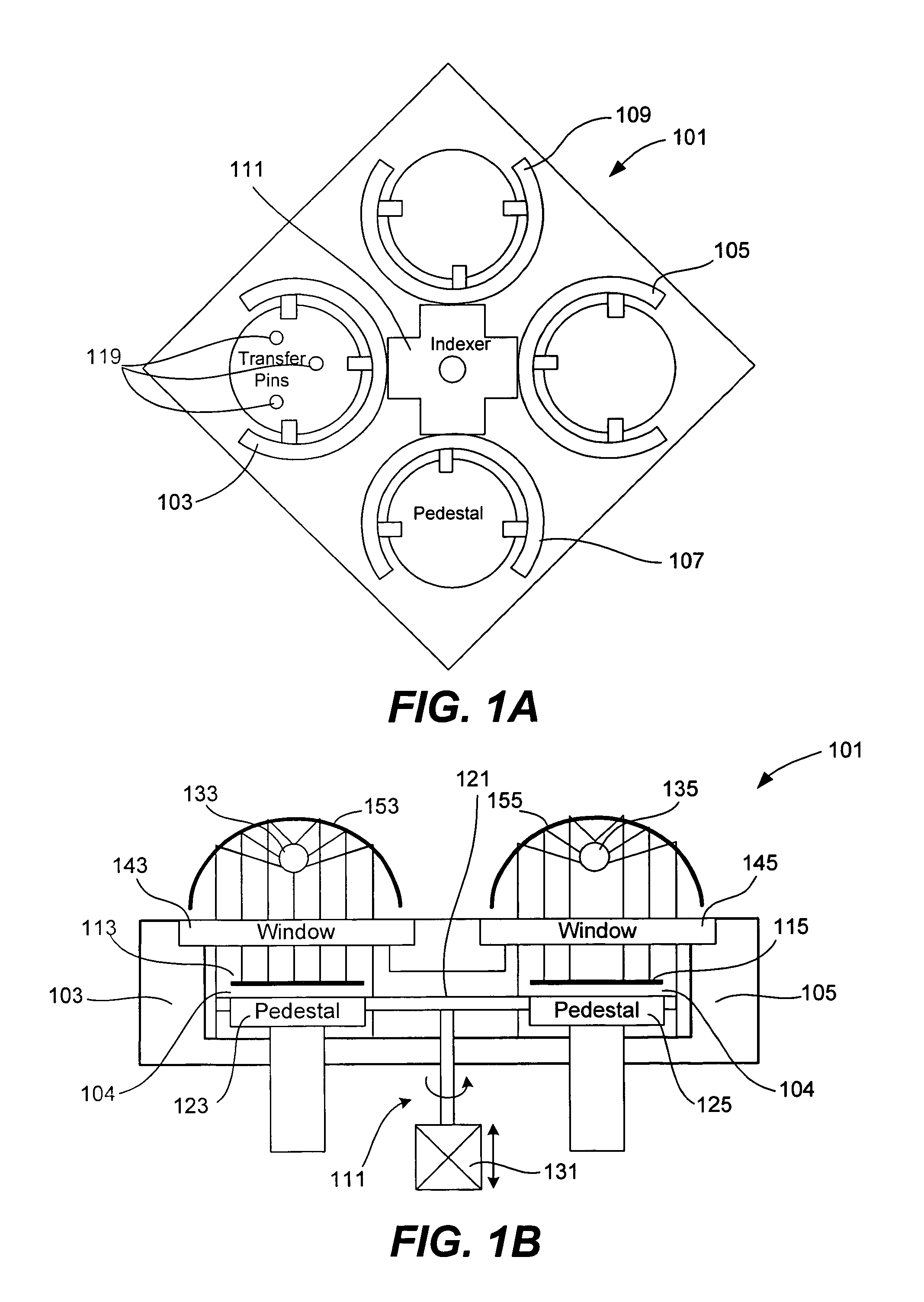
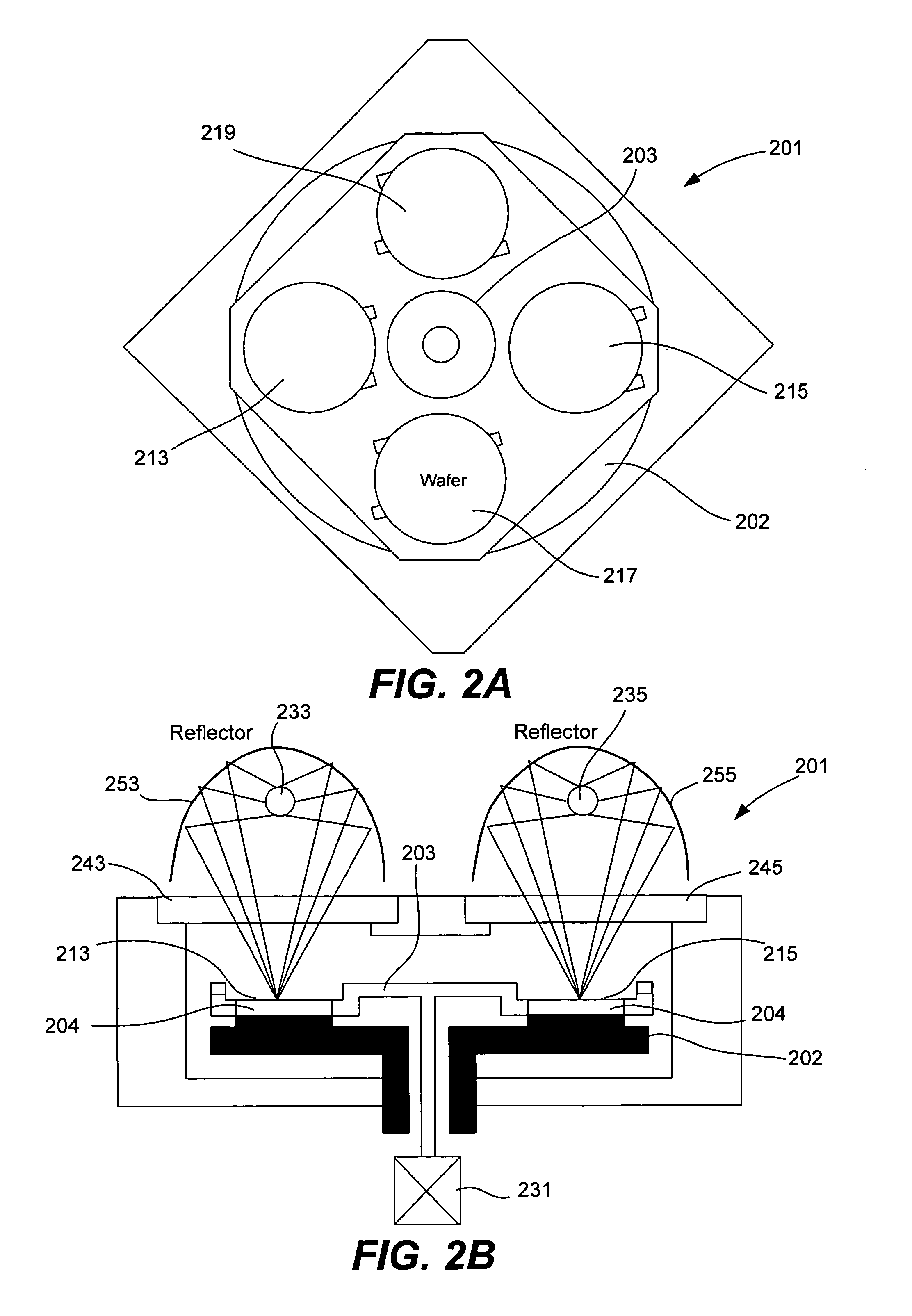

Ultraviolet reflector with coolant gas holes and method
PatentActiveUS20110248183A1
Innovation
- A substrate processing apparatus with a reflector assembly comprising a centrally positioned longitudinal strip and side reflectors, featuring through holes for coolant gas direction and dichroic coatings to enhance UV radiation distribution and cooling, forming a parabolic-type surface to focus coolant gas effectively on the UV lamp, reducing heat accumulation and improving cooling efficiency.


Environmental Impact of UV Curing Processes
UV curing processes in wafer reconstitution have emerged as critical manufacturing steps that require careful environmental consideration. The semiconductor industry's growing emphasis on sustainability has brought increased scrutiny to the environmental footprint of these processes, particularly regarding energy consumption, chemical emissions, and waste generation patterns.
Energy consumption represents the most significant environmental impact of UV curing systems. Traditional mercury-based UV lamps consume substantial electrical power, typically ranging from 200 to 400 watts per inch of lamp length, with efficiency rates often below 15%. This high energy demand translates directly to increased carbon emissions, especially in regions where electricity generation relies heavily on fossil fuels. The continuous operation requirements during wafer processing cycles further amplify these energy-related environmental concerns.
Chemical emissions constitute another major environmental challenge in UV curing applications. Photoinitiators and monomers used in UV-curable materials can release volatile organic compounds during the curing process. These emissions include acrylates, methacrylates, and various photoinitiator byproducts that contribute to air quality degradation and potential workplace exposure risks. The confined nature of semiconductor fabrication facilities necessitates sophisticated ventilation systems, which themselves consume additional energy while managing these emissions.
Waste generation from UV curing processes encompasses both material waste and equipment disposal concerns. Uncured or partially cured materials often require disposal as hazardous waste due to their chemical composition. Mercury-containing UV lamps present particular disposal challenges, requiring specialized handling procedures to prevent environmental contamination. The relatively short lifespan of UV lamps, typically 1000-2000 hours, creates ongoing waste streams that must be managed appropriately.
Recent regulatory developments have intensified focus on environmental compliance in semiconductor manufacturing. The European Union's REACH regulations and similar frameworks in other regions impose strict requirements on chemical usage and emission control. These regulations directly impact UV curing process design and operation, driving manufacturers toward more environmentally sustainable approaches while maintaining production quality standards.
Quality Control Standards for UV Cured Wafers
Quality control standards for UV cured wafers in reconstitution processes require comprehensive evaluation frameworks that address both material integrity and process consistency. These standards must encompass multiple dimensional aspects including adhesion strength, thermal stability, electrical properties, and mechanical durability to ensure reliable semiconductor packaging performance.
Adhesion strength testing represents a fundamental quality metric, typically measured through die shear and wire bond pull tests. Industry standards mandate minimum adhesion values of 5-10 kg-force for die attachment, depending on package size and application requirements. Cross-hatch adhesion tests following ASTM D3359 protocols provide additional validation for polymer-substrate interfaces, with acceptable ratings typically ranging from 3B to 5B classification levels.
Thermal cycling qualification standards require UV cured wafers to withstand temperature excursions from -55°C to +150°C for minimum 1000 cycles without delamination or cracking. Glass transition temperature measurements via differential scanning calorimetry must demonstrate Tg values exceeding operational temperature ranges by at least 50°C margin to ensure long-term reliability under thermal stress conditions.
Electrical performance criteria focus on maintaining low moisture absorption rates below 0.5% and dielectric constant stability within ±5% variation across frequency ranges from 1MHz to 10GHz. Insulation resistance measurements must exceed 10^12 ohms-cm at 85°C/85% relative humidity conditions after 168-hour exposure testing.
Mechanical property standards encompass flexural strength requirements exceeding 100 MPa and elastic modulus values between 2-8 GPa, depending on specific application demands. Coefficient of thermal expansion matching within ±5 ppm/°C of substrate materials prevents stress-induced failures during thermal processing steps.
Process control parameters include real-time monitoring of UV dose uniformity across wafer surfaces, with acceptable variation limits typically maintained within ±10% of target exposure values. Spectral irradiance verification ensures consistent wavelength distribution, particularly critical for photoinitiator activation efficiency in the 365-405nm range commonly employed in semiconductor applications.
Unlock deeper insights with PatSnap Eureka Quick Research — get a full tech report to explore trends and direct your research. Try now!
Generate Your Research Report Instantly with AI Agent
Supercharge your innovation with PatSnap Eureka AI Agent Platform!