

How To Overcome Surface Roughness Challenges In Electron Beam Patterns
APR 28, 20268 MIN READ
Generate Your Research Report Instantly with AI Agent
PatSnap Eureka helps you evaluate technical feasibility & market potential.
Electron Beam Patterning Surface Roughness Background and Goals
Electron beam lithography has emerged as a cornerstone technology in nanofabrication, enabling the creation of patterns with sub-10 nanometer resolution. However, surface roughness remains one of the most persistent challenges limiting the widespread adoption of this technology in high-volume manufacturing. The evolution of electron beam patterning began in the 1960s with early scanning electron microscopes adapted for lithographic purposes, progressing through decades of refinement in beam control, resist chemistry, and substrate preparation techniques.
The fundamental challenge of surface roughness in electron beam patterns stems from multiple interconnected factors. Line edge roughness and line width roughness directly impact device performance in semiconductor applications, particularly as feature sizes continue to shrink below 7 nanometers. These roughness variations can cause significant electrical parameter variations in transistors, memory devices, and interconnects, ultimately affecting yield and reliability.
Current technological trends indicate an increasing demand for smoother pattern edges as the industry pushes toward 3-nanometer and beyond process nodes. The International Technology Roadmap for Semiconductors has identified surface roughness control as a critical enablement requirement for future generations of electronic devices. Advanced applications in quantum computing, photonics, and biotechnology also demand unprecedented pattern fidelity and surface smoothness.
The primary technical objectives in addressing surface roughness challenges encompass several key areas. First, achieving sub-nanometer line edge roughness while maintaining high throughput represents a fundamental goal. This requires optimization of resist materials, development processes, and beam parameters. Second, establishing predictable and controllable roughness characteristics across different substrate materials and pattern geometries is essential for manufacturing scalability.
Another critical objective involves developing comprehensive metrology and characterization techniques capable of accurately measuring and predicting roughness behavior at the atomic scale. This includes real-time monitoring capabilities during the patterning process and post-processing analysis tools that can correlate roughness parameters with device performance metrics.
The ultimate goal extends beyond mere roughness reduction to achieving deterministic control over surface morphology. This involves understanding and manipulating the fundamental physical and chemical processes that govern pattern formation, including electron-resist interactions, molecular diffusion during development, and substrate-resist interface effects. Success in these areas will enable electron beam lithography to fulfill its potential as a viable manufacturing technology for next-generation nanoelectronic devices.
Market Demand for High-Precision Electron Beam Lithography
The semiconductor industry's relentless pursuit of smaller feature sizes and higher device densities has created an unprecedented demand for high-precision electron beam lithography systems. As traditional photolithography approaches its physical limits, electron beam lithography emerges as the critical enabling technology for next-generation semiconductor manufacturing, particularly for advanced nodes below 7nm and emerging applications in quantum computing and photonics.
The market demand is primarily driven by the semiconductor sector's need to overcome the limitations of conventional optical lithography. Leading foundries and integrated device manufacturers require electron beam systems capable of producing sub-10nm features with exceptional accuracy and minimal surface roughness. This demand extends beyond traditional CMOS applications to include specialized markets such as MEMS devices, advanced packaging, and research institutions developing novel nanostructures.
Surface roughness challenges in electron beam patterning directly impact yield rates and device performance, making precision control a critical market differentiator. Manufacturers are increasingly seeking solutions that can achieve line edge roughness values below 2nm while maintaining high throughput capabilities. The growing complexity of three-dimensional device architectures further amplifies the need for precise surface control in electron beam lithography processes.
The automotive electronics sector represents an emerging demand driver, particularly for advanced driver assistance systems and autonomous vehicle technologies that require high-reliability semiconductor components with stringent surface quality specifications. Similarly, the expanding 5G infrastructure market demands precise electron beam lithography for manufacturing high-frequency components and advanced antenna systems.
Market growth is also fueled by the increasing adoption of electron beam lithography in mask making for extreme ultraviolet lithography, where surface roughness directly affects the quality of subsequent photolithography processes. Research and development activities in quantum technologies, neuromorphic computing, and advanced sensor applications continue to expand the addressable market for high-precision electron beam systems capable of overcoming surface roughness limitations.
Current Surface Roughness Challenges in EBL Systems
Electron beam lithography systems face significant surface roughness challenges that fundamentally limit pattern fidelity and resolution capabilities. The primary manifestation occurs through line edge roughness (LER) and linewidth roughness (LWR), where pattern boundaries deviate from their intended smooth profiles. These deviations typically range from 2-5 nanometers in advanced systems, creating substantial obstacles for sub-10nm feature fabrication.
Shot noise represents the most fundamental challenge in EBL surface roughness. The discrete nature of electron interactions with resist materials creates statistical variations in exposure dose distribution. This quantum-level uncertainty becomes increasingly problematic as feature sizes shrink, since the relative impact of individual electron events grows proportionally larger. The stochastic nature of this phenomenon makes it particularly difficult to eliminate through conventional process optimization.
Resist material properties contribute significantly to surface roughness challenges. Polymer chain entanglement and molecular weight distribution create inherent roughness sources during development processes. Chemical amplification resists, while offering high sensitivity, introduce additional roughness through acid diffusion mechanisms that blur pattern edges. The trade-off between sensitivity and resolution creates a fundamental constraint where higher sensitivity materials typically exhibit increased surface roughness.
Proximity effects compound surface roughness issues by creating non-uniform exposure distributions. Forward scattering and backscattering of electrons generate complex dose profiles that vary with local pattern density and substrate composition. These effects create systematic variations in pattern dimensions and edge quality, particularly problematic in dense pattern arrays where neighboring features influence each other's exposure characteristics.
Substrate interactions present another critical challenge category. Different substrate materials exhibit varying backscattering coefficients, creating dose non-uniformities that translate directly into surface roughness variations. Multi-layer substrates compound this issue through complex electron interaction volumes that extend several micrometers below the resist surface.
Process-induced roughness emerges from development chemistry and environmental factors. Temperature fluctuations, developer concentration variations, and contamination introduce additional roughness sources that overlay the fundamental exposure-related challenges. Vibration and electromagnetic interference during exposure further degrade pattern quality through beam positioning errors.
The cumulative effect of these challenges creates a complex optimization landscape where improvements in one area often exacerbate problems in others, necessitating comprehensive systematic approaches to achieve meaningful surface roughness reductions in next-generation EBL applications.
Existing Solutions for Surface Roughness Mitigation
01 Electron beam lithography for surface patterning
Electron beam lithography techniques are used to create precise patterns on surfaces by controlling the electron beam exposure. This method allows for high-resolution patterning with controlled surface roughness characteristics. The process involves directing focused electron beams to selectively modify surface properties and create desired topographical features.- Electron beam lithography for surface patterning: Electron beam lithography techniques are used to create precise patterns on surfaces by controlling the electron beam exposure. This method allows for high-resolution patterning and can be used to modify surface roughness characteristics through controlled material removal or deposition. The process involves scanning an electron beam across a substrate to create desired surface topographies and patterns with nanometer-scale precision.
- Surface roughness measurement using electron beam techniques: Electron beam-based methods are employed to measure and analyze surface roughness parameters. These techniques utilize the interaction between electron beams and surface features to determine roughness characteristics, providing detailed topographical information. The measurement systems can detect minute surface variations and provide quantitative data about surface texture and morphology.
- Electron beam processing for surface modification: Electron beam processing techniques are used to modify surface properties and roughness through controlled energy deposition. This approach can alter material structure, create specific surface textures, or remove material to achieve desired roughness levels. The process parameters such as beam current, voltage, and scanning speed can be optimized to control the resulting surface characteristics.
- Pattern formation on rough surfaces using electron beams: Methods for creating patterns on surfaces with existing roughness using electron beam technology. These techniques account for surface irregularities and adapt the patterning process to achieve uniform results despite substrate roughness variations. The approaches include compensation algorithms and adaptive exposure strategies to maintain pattern fidelity on non-ideal surfaces.
- Control systems for electron beam surface processing: Advanced control systems and feedback mechanisms for managing electron beam parameters during surface processing operations. These systems monitor and adjust beam characteristics in real-time to maintain consistent surface modification results. The control methods include automated positioning, beam intensity regulation, and process parameter optimization to achieve desired surface roughness outcomes.
02 Surface roughness measurement and characterization
Methods for measuring and characterizing surface roughness created by electron beam processes involve various analytical techniques. These approaches enable quantitative assessment of surface topography and roughness parameters. The characterization methods help optimize electron beam parameters for achieving desired surface properties.Expand Specific Solutions03 Electron beam processing parameters optimization
Optimization of electron beam processing parameters such as beam current, acceleration voltage, and scanning patterns to control surface roughness. The relationship between beam parameters and resulting surface characteristics is critical for achieving consistent and predictable roughness patterns. Process control methods ensure reproducible surface modification results.Expand Specific Solutions04 Surface modification through electron beam irradiation
Electron beam irradiation techniques for modifying surface properties and creating controlled roughness patterns. The process involves using electron beams to alter material surface structure and topography. Various irradiation strategies can be employed to achieve specific surface roughness characteristics for different applications.Expand Specific Solutions05 Applications of electron beam patterned surfaces
Applications utilizing electron beam patterned surfaces with controlled roughness for various industrial and technological purposes. These applications benefit from the precise control over surface topography that electron beam processing provides. The patterned surfaces find use in optical devices, microelectronics, and specialized coatings where specific roughness characteristics are required.Expand Specific Solutions
Key Players in Electron Beam Lithography Industry
The electron beam patterning surface roughness challenge represents a mature yet evolving technological landscape within the advanced semiconductor and nanofabrication industry. The market demonstrates significant scale, driven by increasing demand for precision manufacturing in electronics, with established players like Samsung Electronics, Toshiba, and GLOBALFOUNDRIES leading semiconductor applications, while specialized companies such as NIL Technology and Tokyo Ohka Kogyo focus on lithography solutions. Technology maturity varies across segments, with traditional photoresist and chemical processing approaches from Shin-Etsu Chemical and FUJIFILM showing high maturity, while emerging nanoimprint and advanced surface treatment technologies remain in development phases. The competitive landscape spans from large integrated manufacturers to specialized materials companies, indicating a fragmented but innovation-driven market addressing critical precision manufacturing requirements across multiple high-tech industries.
Samsung Electronics Co., Ltd.
Technical Solution: Samsung has developed advanced electron beam lithography (EBL) techniques combined with surface treatment processes to minimize roughness in nanoscale patterning. Their approach involves multi-step resist processing with optimized exposure parameters and post-exposure treatments. The company utilizes proximity effect correction algorithms and variable-shaped beam writing strategies to achieve sub-10nm resolution while maintaining low line edge roughness. Samsung's methodology includes surface preparation techniques using plasma cleaning and chemical treatments to reduce substrate roughness before EBL exposure, resulting in improved pattern fidelity for semiconductor device manufacturing.
Strengths: Industry-leading resolution capabilities, extensive R&D resources, proven manufacturing scalability. Weaknesses: High equipment costs, complex process optimization requirements.
Varian Semiconductor Equipment Associates, Inc.
Technical Solution: Varian specializes in ion beam surface modification techniques that complement electron beam patterning by pre-treating surfaces to reduce roughness. Their ion implantation systems can create atomically smooth surfaces through controlled bombardment and annealing processes. The company's approach involves using low-energy ion beams to selectively modify surface properties, creating uniform nucleation sites for subsequent electron beam patterning. This technique significantly reduces surface roughness variations and improves pattern uniformity across large substrate areas, particularly beneficial for high-volume semiconductor manufacturing applications.
Strengths: Specialized ion beam expertise, proven surface modification capabilities, industrial-scale equipment. Weaknesses: Limited to surface pre-treatment applications, requires integration with EBL systems.
Core Innovations in EBL Surface Quality Control
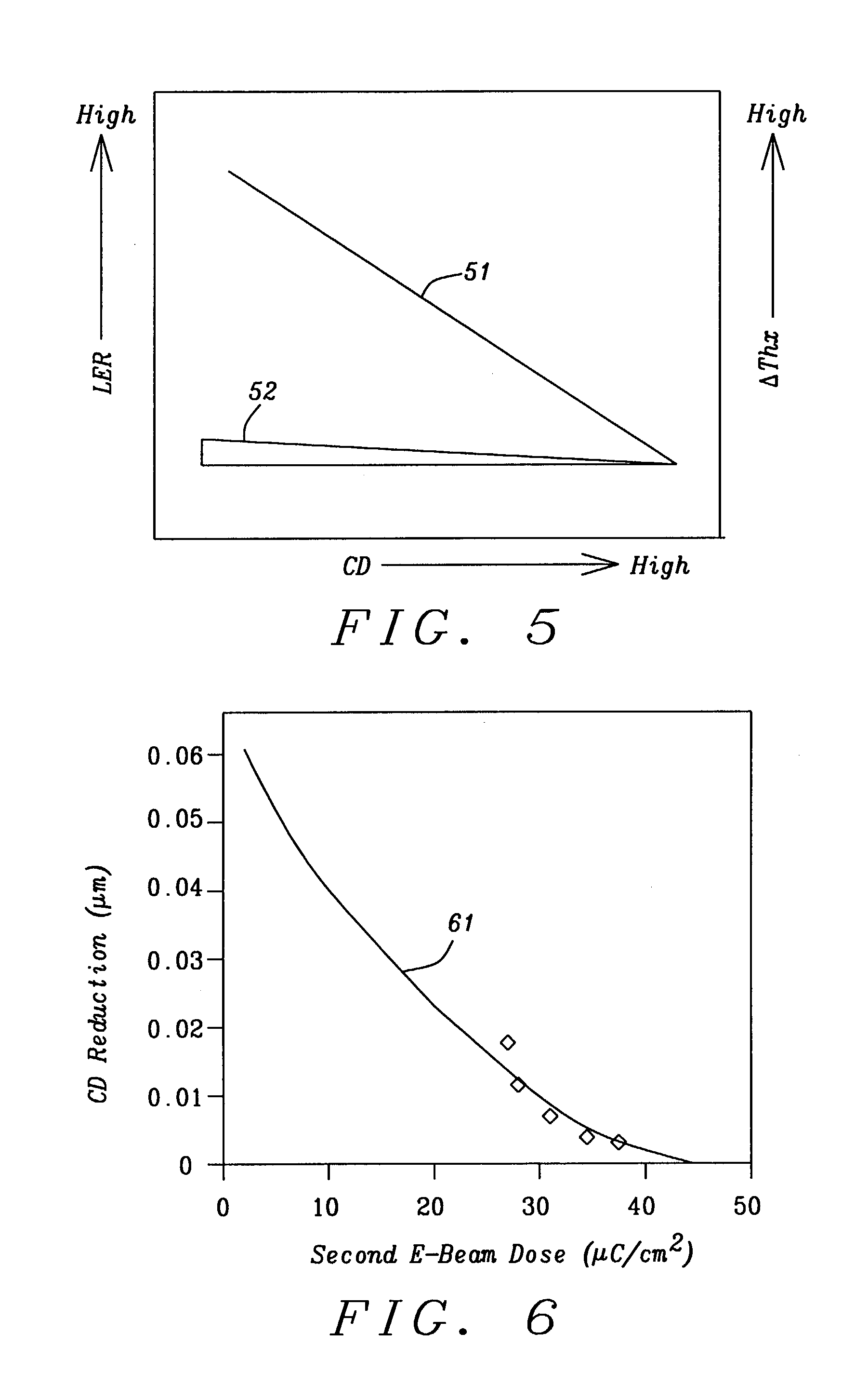
Method to form reduced dimension pattern with good edge roughness
PatentInactiveUS20040214109A1
Innovation
- A secondary electron beam exposure is applied to the developed resist pattern, followed by a longer heat treatment and a stronger development process, which reduces edge roughness and allows controlled CD reduction by dissolving only the edges with a concentrated developer, preserving the feature shape and resist thickness.
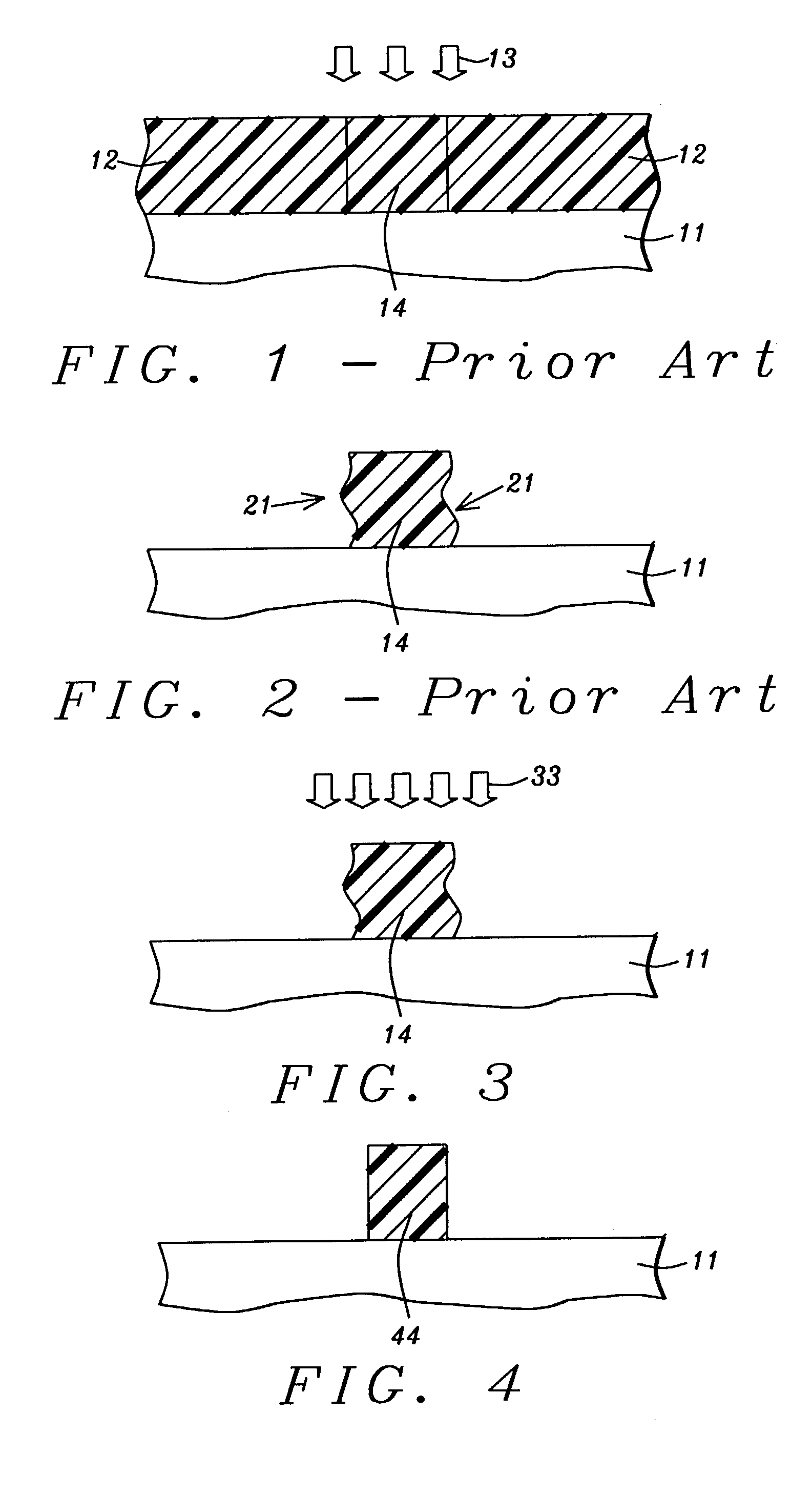
Method for surface treatment with electron beam and apparatus for surface treatment with electron beam
PatentWO2007083363A1
Innovation
- An electron beam surface treatment method and apparatus that scans the surface two-dimensionally along a curved trajectory, allowing the surface layer to melt and solidify uniformly, with controlled beam convergence and deflection to maintain consistent energy density, thereby achieving a fine surface roughness of about 1 μm in a short time and ensuring uniformity across the entire treated area.


Advanced Resist Materials for Smooth Pattern Formation
Advanced resist materials represent a critical frontier in addressing surface roughness challenges inherent in electron beam lithography processes. Traditional photoresists often exhibit molecular-level heterogeneity that translates directly into pattern edge roughness, necessitating the development of next-generation materials with enhanced uniformity and processing characteristics.
Molecular glass resists have emerged as promising candidates for achieving superior pattern smoothness. These materials feature well-defined molecular structures with uniform size distribution, eliminating the polydispersity issues associated with conventional polymer resists. The controlled molecular architecture enables more predictable dissolution behavior during development, resulting in significantly reduced line edge roughness values typically below 2 nanometers.
Inorganic resist systems, particularly metal oxide-based materials, offer another pathway toward smooth pattern formation. These resists demonstrate exceptional resolution capabilities while maintaining low surface roughness due to their inherently uniform atomic structure. Hafnium oxide and zinc oxide-based formulations have shown particular promise, exhibiting both high sensitivity to electron beam exposure and excellent pattern fidelity.
Hybrid organic-inorganic resist materials combine the processing advantages of organic polymers with the structural uniformity of inorganic components. These systems typically incorporate metal-containing precursors within organic matrices, enabling selective cross-linking or degradation upon electron beam exposure while maintaining smooth pattern edges through controlled phase separation mechanisms.
Advanced chemically amplified resists with optimized acid generator distribution represent another significant development. By employing novel photoacid generators with improved spatial distribution and controlled diffusion characteristics, these materials minimize the stochastic variations that contribute to surface roughness. Enhanced base quencher systems further refine the chemical contrast, leading to sharper pattern boundaries.
Surface modification approaches using self-assembled monolayers and brush polymers provide additional smoothing mechanisms. These treatments can be applied either as underlayers to promote uniform resist coating or as post-development treatments to reduce existing roughness through controlled swelling and relaxation processes.
Process Optimization Strategies for EBL Quality Enhancement
Process optimization in electron beam lithography represents a systematic approach to minimizing surface roughness through careful control of exposure parameters and environmental conditions. The fundamental strategy involves establishing optimal dose distributions that ensure complete resist development while preventing overexposure effects that contribute to edge roughness. Critical parameters include beam current stability, writing speed optimization, and precise dose modulation across different pattern geometries.
Resist processing optimization forms the cornerstone of surface quality enhancement. Pre-exposure treatments such as substrate cleaning protocols and resist film thickness uniformity directly impact final pattern fidelity. Post-exposure baking temperatures and durations require precise calibration to minimize thermal stress-induced deformations. Development process optimization involves controlling developer concentration, temperature, and agitation patterns to achieve uniform material removal rates across the entire substrate surface.
Advanced beam shaping techniques offer significant improvements in pattern quality through optimized exposure strategies. Variable-shaped beam systems enable precise control over dose distribution at pattern edges, reducing proximity effects that contribute to roughness. Multi-pass exposure strategies with reduced individual doses help minimize charging effects and thermal damage, particularly beneficial for sensitive substrates and high-aspect-ratio structures.
Environmental control optimization addresses external factors affecting pattern quality. Vibration isolation systems, temperature stability within ±0.1°C, and electromagnetic interference shielding create optimal conditions for precise beam positioning. Chamber pressure maintenance below 10^-6 Torr prevents contamination-induced roughness while ensuring stable electron optics performance.
Real-time process monitoring integration enables dynamic optimization during exposure. Beam drift correction systems, automatic focus adjustment, and dose feedback mechanisms maintain consistent writing conditions throughout extended lithography sessions. Statistical process control implementation tracks key performance indicators, enabling predictive maintenance and process drift detection before quality degradation occurs.
Unlock deeper insights with PatSnap Eureka Quick Research — get a full tech report to explore trends and direct your research. Try now!
Generate Your Research Report Instantly with AI Agent
Supercharge your innovation with PatSnap Eureka AI Agent Platform!