

How to Reduce Ferroelectric Memory Write Disturbance Effects
JUN 3, 20269 MIN READ
Generate Your Research Report Instantly with AI Agent
PatSnap Eureka helps you evaluate technical feasibility & market potential.
Ferroelectric Memory Write Disturbance Background and Objectives
Ferroelectric memory technology has emerged as a promising non-volatile memory solution, combining the speed advantages of DRAM with the data retention capabilities of flash memory. The fundamental principle relies on ferroelectric materials that can maintain polarization states even without power, enabling rapid read/write operations while preserving data integrity. However, the practical implementation of ferroelectric memory faces significant challenges, particularly in the form of write disturbance effects that compromise memory reliability and performance.
Write disturbance in ferroelectric memory occurs when programming operations on target cells inadvertently affect neighboring cells, leading to data corruption or degradation. This phenomenon stems from the inherent characteristics of ferroelectric materials and the architectural constraints of memory arrays. During write operations, the electric fields required to switch ferroelectric polarization can extend beyond the intended cell boundaries, causing unintended polarization changes in adjacent cells.
The severity of write disturbance effects has intensified with the continuous scaling of memory devices and increasing integration density. As cell dimensions shrink and array structures become more compact, the proximity between memory elements increases the likelihood of cross-coupling effects. Additionally, the variability in ferroelectric material properties across different cells can exacerbate disturbance sensitivity, creating non-uniform response patterns that complicate mitigation strategies.
Current industry trends indicate a growing demand for high-density, low-power memory solutions in applications ranging from mobile devices to automotive systems and IoT devices. Ferroelectric memory technology holds significant potential to address these requirements, but the write disturbance challenge remains a critical barrier to widespread commercial adoption. The technology's success depends heavily on developing effective solutions that can minimize disturbance effects while maintaining the inherent advantages of ferroelectric materials.
The primary objective of addressing write disturbance effects is to achieve reliable memory operation with minimal data corruption rates, typically targeting bit error rates below industry-standard thresholds. Secondary objectives include maintaining fast write speeds, reducing power consumption, and ensuring long-term endurance characteristics. These goals must be balanced against manufacturing complexity and cost considerations to enable commercially viable ferroelectric memory products.
Market Demand for Reliable Ferroelectric Memory Solutions
The global ferroelectric memory market is experiencing unprecedented growth driven by the increasing demand for non-volatile memory solutions that combine high-speed operation with low power consumption. Industries ranging from automotive electronics to Internet of Things devices require memory technologies that can maintain data integrity while operating under harsh environmental conditions and frequent write operations.
Enterprise storage systems represent a particularly lucrative segment where ferroelectric memory solutions are gaining traction. Data centers and cloud computing infrastructure providers are actively seeking alternatives to traditional flash memory to address performance bottlenecks and reduce energy consumption. The ability of ferroelectric memory to perform write operations without the erase cycles required by flash memory makes it an attractive option for applications requiring frequent data updates.
The automotive sector has emerged as a critical driver for reliable ferroelectric memory solutions, particularly with the advancement of autonomous driving technologies and advanced driver assistance systems. These applications demand memory devices that can withstand extreme temperature variations while maintaining consistent performance and data reliability. Write disturbance effects in such safety-critical applications could lead to catastrophic failures, making disturbance-resistant ferroelectric memory solutions essential.
Consumer electronics manufacturers are increasingly incorporating ferroelectric memory into wearable devices, smart sensors, and mobile applications where battery life and instant-on capabilities are paramount. The market demand in this sector is particularly focused on memory solutions that can minimize write disturbance while maintaining ultra-low power consumption during both active and standby modes.
Industrial automation and smart manufacturing applications represent another significant market segment driving demand for robust ferroelectric memory solutions. These environments require memory devices that can operate reliably in the presence of electromagnetic interference and mechanical vibrations while maintaining data integrity across millions of write cycles. The ability to reduce write disturbance effects directly translates to improved system reliability and reduced maintenance costs in industrial settings.
The telecommunications infrastructure sector, particularly with the rollout of 5G networks and edge computing nodes, requires memory solutions that can handle high-frequency data transactions without compromising neighboring memory cells. Network equipment manufacturers are actively seeking ferroelectric memory technologies that demonstrate superior write disturbance immunity to ensure consistent network performance and minimize data corruption risks.
Current State and Challenges of Write Disturbance in FeRAM
Ferroelectric Random Access Memory (FeRAM) technology has reached a critical juncture where write disturbance effects represent one of the most significant barriers to widespread adoption and scaling. Current FeRAM implementations demonstrate excellent endurance and speed characteristics, yet suffer from inherent vulnerabilities during write operations that compromise data integrity in adjacent cells.
The fundamental challenge stems from the capacitive coupling between neighboring ferroelectric cells during polarization switching. When a write voltage is applied to a target cell, parasitic electric fields inevitably affect surrounding cells, potentially causing unwanted polarization reversals or partial switching events. This phenomenon becomes increasingly problematic as memory density increases and cell dimensions shrink below 100 nanometers.
Manufacturing variations in ferroelectric thin films exacerbate the write disturbance problem. Inconsistencies in film thickness, grain structure, and composition create non-uniform coercive field distributions across the memory array. These variations result in some cells being more susceptible to disturbance than others, making it difficult to establish universal operating parameters that ensure reliable operation across the entire memory device.
Temperature dependencies further complicate the current state of FeRAM technology. The coercive field of ferroelectric materials exhibits significant temperature coefficients, meaning that write disturbance susceptibility varies considerably across operating temperature ranges. This thermal sensitivity requires complex compensation mechanisms and limits the operational envelope of FeRAM devices in demanding applications.
Cross-talk between word lines and bit lines during write operations presents another substantial challenge. The three-dimensional electric field distributions created during addressing sequences can induce disturbance effects in cells that share common addressing infrastructure. Current mitigation strategies, including reference voltage schemes and write-back operations, add complexity and reduce overall system performance.
Scaling limitations pose perhaps the greatest long-term challenge for FeRAM technology. As cell sizes approach fundamental physical limits, the energy barriers that separate stable polarization states decrease, making cells increasingly vulnerable to disturbance from neighboring operations. Traditional approaches to disturbance mitigation become less effective at these scales, necessitating entirely new architectural and material solutions.
Existing Write Disturbance Reduction Techniques
01 Write disturbance mitigation through voltage control and pulse optimization
Techniques for reducing write disturbance effects in ferroelectric memory by optimizing write voltage levels, pulse duration, and waveform characteristics. These methods focus on controlling the electrical parameters during write operations to minimize unintended polarization changes in adjacent memory cells while maintaining reliable data storage.- Write disturbance mitigation techniques in ferroelectric memory arrays: Various techniques are employed to reduce write disturbance effects in ferroelectric memory devices, including voltage control methods, pulse optimization, and selective writing schemes. These approaches help minimize unwanted polarization changes in non-selected memory cells during write operations, thereby maintaining data integrity and improving memory reliability.
- Memory cell architecture design for disturbance reduction: Specialized memory cell structures and array architectures are designed to inherently reduce write disturbance effects. These designs include optimized transistor configurations, improved isolation techniques, and enhanced cell layouts that minimize cross-coupling between adjacent cells and reduce parasitic effects during write operations.
- Compensation and correction algorithms for write disturbance: Advanced algorithms and correction schemes are implemented to compensate for write disturbance effects in ferroelectric memories. These methods include error detection and correction codes, adaptive writing strategies, and real-time monitoring systems that can identify and correct disturbance-induced errors to maintain data accuracy.
- Voltage and timing optimization for write operations: Precise control of write voltages, pulse widths, and timing sequences is crucial for minimizing disturbance effects. Optimization techniques include adaptive voltage scaling, multi-level pulse schemes, and sophisticated timing control circuits that ensure proper writing while reducing impact on neighboring cells.
- Reference and sensing schemes for disturbance detection: Specialized reference systems and sensing circuits are developed to detect and measure write disturbance effects in ferroelectric memories. These schemes include reference cell arrays, differential sensing techniques, and monitoring circuits that can identify disturbance patterns and enable corrective actions to maintain memory performance.
02 Memory cell architecture design for disturbance reduction
Structural approaches to minimize write disturbance through specialized memory cell layouts, isolation techniques, and array configurations. These designs incorporate physical barriers and optimized cell geometries to prevent cross-coupling effects between neighboring ferroelectric memory elements during write operations.Expand Specific Solutions03 Compensation and correction algorithms for disturbed data
Software-based solutions that detect and correct data corruption caused by write disturbance effects. These algorithms implement error detection schemes, reference cell monitoring, and adaptive correction mechanisms to maintain data integrity in ferroelectric memory systems despite disturbance-induced changes.Expand Specific Solutions04 Write sequence optimization and scheduling methods
Strategies for organizing write operations in ferroelectric memory to minimize cumulative disturbance effects. These approaches involve intelligent write scheduling, block management techniques, and temporal distribution of write operations to reduce the impact on neighboring cells and maintain overall memory reliability.Expand Specific Solutions05 Reference and sensing circuit improvements for disturbance tolerance
Enhanced sensing and reference circuit designs that improve the detection and measurement of ferroelectric memory states in the presence of write disturbance effects. These circuits provide better noise immunity, improved signal margins, and adaptive threshold adjustment to maintain reliable read operations despite disturbance-induced variations.Expand Specific Solutions
Key Players in Ferroelectric Memory Industry
The ferroelectric memory write disturbance reduction field represents an emerging technology sector within the broader non-volatile memory market, currently in its early-to-mid development stage. The market shows significant growth potential as demand for low-power, high-density memory solutions increases across computing and mobile applications. Technology maturity varies considerably among key players, with established semiconductor giants like Samsung Electronics, Intel, Micron Technology, and Taiwan Semiconductor Manufacturing leading in foundational research and manufacturing capabilities. Asian companies including Huawei Technologies, Sony Semiconductor Solutions, and Toshiba demonstrate strong innovation in device-level solutions, while specialized memory manufacturers like Macronix International focus on application-specific implementations. Research institutions such as Fudan University and Institute of Microelectronics of Chinese Academy of Sciences contribute fundamental breakthroughs in materials science and device physics. The competitive landscape indicates a technology transitioning from laboratory research to commercial viability, with multiple approaches being pursued simultaneously across different market segments.
Texas Instruments Incorporated
Technical Solution: Texas Instruments addresses ferroelectric memory write disturbance through robust analog circuit design and precision control systems. Their solutions feature high-precision voltage regulators and current sources that ensure consistent write conditions across all memory operations. TI implements advanced timing control circuits that optimize write pulse shapes and durations to minimize disturbance effects. The company's approach includes comprehensive characterization of ferroelectric material properties and development of adaptive compensation circuits that account for process variations and aging effects in ferroelectric capacitors.
Strengths: Excellence in analog circuit design, strong automotive and industrial market presence, reliable manufacturing processes. Weaknesses: Smaller scale in advanced memory technologies, limited resources compared to major memory manufacturers.
Intel Corp.
Technical Solution: Intel's ferroelectric memory solutions address write disturbance through advanced circuit design and system-level optimizations. Their technology incorporates intelligent write scheduling algorithms that minimize simultaneous operations on adjacent memory cells. Intel has developed specialized sense amplifier designs with enhanced noise immunity and implements dynamic voltage scaling techniques to optimize write operations. The company's approach includes comprehensive modeling of ferroelectric switching dynamics to predict and prevent disturbance patterns, combined with machine learning algorithms that adapt write parameters based on usage patterns and environmental conditions.
Strengths: Strong processor integration capabilities, advanced semiconductor manufacturing, extensive system-level expertise. Weaknesses: Limited focus on standalone memory products, high complexity in integration solutions.
Core Patents in Ferroelectric Write Disturbance Solutions
Method and apparatus to reduce storage node disturbance in ferroelectric memory
PatentInactiveUS7133304B2
Innovation
- The method involves selectively pulsing non-selected wordlines to discharge storage nodes while the associated bitlines and platelines are held at a consistent voltage, either during or after memory access operations, to mitigate charge disturbances and maintain signal integrity. This can be implemented in various array architectures, including open and folded bitline configurations, and is applicable to different cell types such as 1T1C and 2T2C.
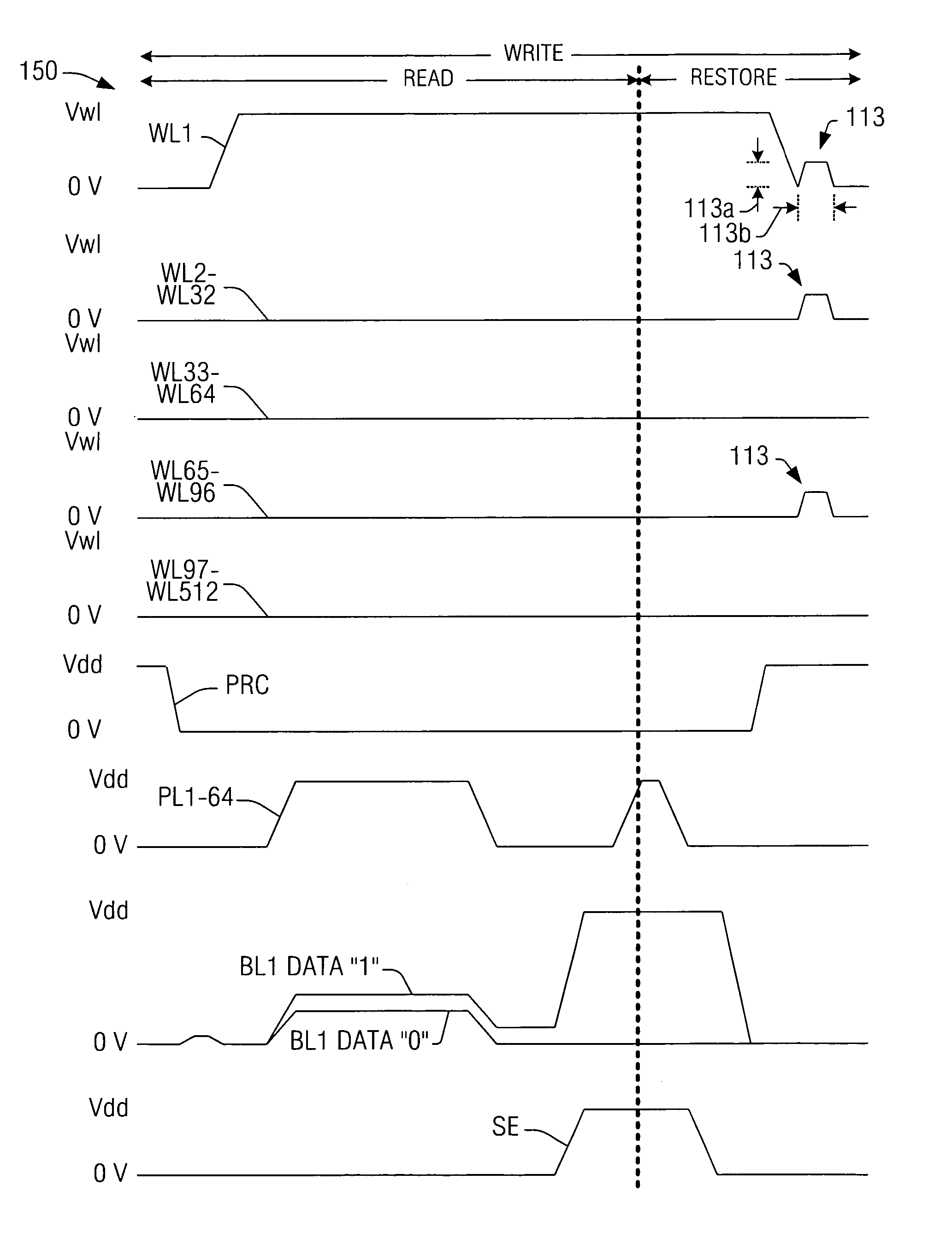

Plateline voltage pulsing to reduce storage node disturbance in ferroelectric memory
PatentInactiveUS7193880B2
Innovation
- Applying selective pulses to non-selected platelines during memory access operations to bias the storage nodes of non-selected ferroelectric memory cells, thereby mitigating charge exchange and leakage, which can be implemented in various array architectures and cell types, including 1T1C and 2T2C configurations.


Memory Reliability Standards and Testing Protocols
Memory reliability standards for ferroelectric memory devices have evolved significantly to address write disturbance effects and ensure consistent performance across various operating conditions. The Joint Electron Device Engineering Council (JEDEC) has established comprehensive guidelines specifically targeting ferroelectric random access memory (FeRAM) reliability, including JESD84 and JESD47 standards that define acceptable failure rates and endurance requirements. These standards mandate specific testing protocols for write disturbance characterization, requiring manufacturers to demonstrate memory cell stability under repeated write operations to adjacent cells.
International standards organizations, including the International Electrotechnical Commission (IEC) and IEEE, have developed complementary frameworks focusing on ferroelectric memory reliability assessment. IEC 62047 series standards provide detailed methodologies for evaluating polarization fatigue and imprint effects, which are critical factors contributing to write disturbance phenomena. These standards establish baseline requirements for retention testing, endurance cycling, and environmental stress screening that directly impact write disturbance mitigation strategies.
Testing protocols for write disturbance evaluation typically employ accelerated stress testing methodologies that simulate years of operation within compressed timeframes. Standard test procedures include checkerboard pattern writing, where alternating data patterns are repeatedly written to assess cross-coupling effects between adjacent memory cells. Temperature cycling tests between -40°C and +125°C combined with voltage stress conditions help identify thermal-induced write disturbance mechanisms and establish operating margins for reliable device performance.
Advanced characterization techniques specified in current standards include pulse-based testing protocols that measure polarization switching dynamics and coercive field variations across memory arrays. These protocols require precise timing measurements to capture transient effects during write operations, enabling identification of optimal pulse shapes and durations that minimize disturbance to neighboring cells. Statistical analysis methods defined in reliability standards ensure adequate sample sizes and confidence levels for meaningful write disturbance assessment.
Emerging testing methodologies focus on real-time monitoring of ferroelectric domain switching behavior using specialized equipment capable of measuring picoampere-level currents during write operations. These advanced protocols enable detection of subtle write disturbance effects that traditional testing methods might overlook, providing deeper insights into failure mechanisms and supporting development of more robust memory architectures with enhanced immunity to write disturbance phenomena.
Circuit Design Optimization for Disturbance Immunity
Circuit design optimization represents a critical approach to mitigating write disturbance effects in ferroelectric memory systems through strategic architectural modifications and enhanced immunity mechanisms. The fundamental principle involves redesigning peripheral circuits and memory cell architectures to minimize unwanted voltage coupling and parasitic effects that contribute to disturbance phenomena.
Voltage regulation circuits play a pivotal role in disturbance immunity enhancement. Advanced voltage reference generators with improved power supply rejection ratios can significantly reduce noise propagation during write operations. These circuits incorporate bandgap references with temperature compensation and low-dropout regulators specifically tuned for ferroelectric memory requirements. The implementation of dedicated voltage domains for different memory operations ensures that write pulses do not interfere with adjacent cells through supply line coupling.
Sense amplifier optimization constitutes another crucial aspect of circuit-level disturbance mitigation. Modern designs employ differential sensing architectures with enhanced common-mode rejection capabilities, effectively filtering out disturbance-induced voltage fluctuations. Cross-coupled latch configurations with adjustable sensitivity thresholds allow for dynamic adaptation to varying disturbance conditions while maintaining reliable read operations.
Write driver circuit modifications focus on pulse shaping and timing control to minimize electromagnetic interference and capacitive coupling effects. Slew rate control circuits ensure that voltage transitions occur within optimal timeframes, reducing the likelihood of inducing disturbances in neighboring cells. Additionally, implementing complementary write schemes with balanced differential signaling helps cancel out common-mode disturbances.
Substrate isolation techniques and guard ring implementations provide physical barriers against electrical coupling between memory cells and peripheral circuits. These design elements create localized electric field containment, preventing disturbance propagation through substrate paths. Advanced layout strategies incorporate strategic placement of decoupling capacitors and power distribution networks optimized for ferroelectric memory characteristics.
Error correction integration at the circuit level enables real-time disturbance detection and compensation. Hardware-based error detection circuits can identify disturbance-induced bit flips and trigger corrective actions without system intervention. This approach combines predictive algorithms with adaptive threshold adjustment mechanisms to maintain data integrity under varying operational conditions.
Unlock deeper insights with PatSnap Eureka Quick Research — get a full tech report to explore trends and direct your research. Try now!
Generate Your Research Report Instantly with AI Agent
Supercharge your innovation with PatSnap Eureka AI Agent Platform!