

Improving Dielectric Constants in Silicon Capacitors for Advanced Computing
MAY 9, 202610 MIN READ
Generate Your Research Report Instantly with AI Agent
PatSnap Eureka helps you evaluate technical feasibility & market potential.
Silicon Capacitor Dielectric Enhancement Background and Objectives
Silicon capacitors have emerged as critical components in advanced computing systems, where the relentless pursuit of higher performance and miniaturization demands increasingly sophisticated dielectric materials. The evolution of silicon-based capacitor technology traces back to the early days of semiconductor manufacturing, where simple silicon dioxide served as the primary dielectric material. However, as computing architectures have advanced toward multi-core processors, artificial intelligence accelerators, and quantum computing platforms, the limitations of traditional dielectric materials have become increasingly apparent.
The fundamental challenge lies in the inverse relationship between capacitor size and performance requirements in modern computing applications. As transistor dimensions continue to shrink following Moore's Law principles, the available space for capacitive elements decreases proportionally, yet the demand for higher capacitance density and improved electrical performance continues to escalate. This technological tension has driven the semiconductor industry to explore novel approaches for enhancing dielectric constants while maintaining the manufacturing compatibility and reliability standards essential for commercial viability.
Contemporary advanced computing systems, including high-performance processors, graphics processing units, and specialized AI chips, require capacitors that can operate at increasingly higher frequencies while maintaining stable electrical characteristics. The dielectric constant directly influences the capacitance value, energy storage capacity, and overall electrical efficiency of these components. Traditional silicon dioxide, with its relatively low dielectric constant of approximately 3.9, has proven insufficient for meeting the performance demands of next-generation computing architectures.
The primary objective of silicon capacitor dielectric enhancement research centers on developing materials and manufacturing processes that can achieve significantly higher dielectric constants without compromising other critical performance parameters. Target specifications typically include dielectric constants exceeding 20-50, while maintaining low leakage currents, high breakdown voltages, and excellent thermal stability across the operational temperature ranges encountered in advanced computing environments.
Secondary objectives encompass the integration of enhanced dielectric materials with existing semiconductor manufacturing processes, ensuring compatibility with current fabrication equipment and quality control methodologies. This includes developing deposition techniques, etching processes, and interface engineering approaches that can reliably produce high-quality dielectric layers at the nanoscale dimensions required for modern integrated circuits.
The strategic importance of this technology extends beyond immediate performance improvements, as enhanced dielectric constants enable new architectural possibilities in processor design, memory systems, and specialized computing accelerators that will define the next generation of computational capabilities.
The fundamental challenge lies in the inverse relationship between capacitor size and performance requirements in modern computing applications. As transistor dimensions continue to shrink following Moore's Law principles, the available space for capacitive elements decreases proportionally, yet the demand for higher capacitance density and improved electrical performance continues to escalate. This technological tension has driven the semiconductor industry to explore novel approaches for enhancing dielectric constants while maintaining the manufacturing compatibility and reliability standards essential for commercial viability.
Contemporary advanced computing systems, including high-performance processors, graphics processing units, and specialized AI chips, require capacitors that can operate at increasingly higher frequencies while maintaining stable electrical characteristics. The dielectric constant directly influences the capacitance value, energy storage capacity, and overall electrical efficiency of these components. Traditional silicon dioxide, with its relatively low dielectric constant of approximately 3.9, has proven insufficient for meeting the performance demands of next-generation computing architectures.
The primary objective of silicon capacitor dielectric enhancement research centers on developing materials and manufacturing processes that can achieve significantly higher dielectric constants without compromising other critical performance parameters. Target specifications typically include dielectric constants exceeding 20-50, while maintaining low leakage currents, high breakdown voltages, and excellent thermal stability across the operational temperature ranges encountered in advanced computing environments.
Secondary objectives encompass the integration of enhanced dielectric materials with existing semiconductor manufacturing processes, ensuring compatibility with current fabrication equipment and quality control methodologies. This includes developing deposition techniques, etching processes, and interface engineering approaches that can reliably produce high-quality dielectric layers at the nanoscale dimensions required for modern integrated circuits.
The strategic importance of this technology extends beyond immediate performance improvements, as enhanced dielectric constants enable new architectural possibilities in processor design, memory systems, and specialized computing accelerators that will define the next generation of computational capabilities.
Market Demand for High-K Dielectric Silicon Capacitors
The global semiconductor industry is experiencing unprecedented demand for high-performance computing solutions, driving significant market requirements for advanced silicon capacitors with enhanced dielectric properties. Data centers, artificial intelligence processors, and edge computing devices require increasingly sophisticated energy storage components that can operate at higher frequencies while maintaining stable performance characteristics.
Enterprise computing applications represent the largest market segment for high-K dielectric silicon capacitors. Cloud service providers and hyperscale data centers are continuously upgrading their infrastructure to support growing computational workloads, creating substantial demand for capacitors that can deliver superior energy density and thermal stability. These applications require components capable of handling rapid charge-discharge cycles while maintaining consistent dielectric performance across varying operating conditions.
The automotive electronics sector is emerging as a rapidly expanding market for advanced silicon capacitors. Electric vehicles and autonomous driving systems demand reliable energy storage solutions that can withstand harsh environmental conditions while providing consistent performance. Advanced driver assistance systems and in-vehicle computing platforms require capacitors with high dielectric constants to support real-time processing capabilities and sensor integration.
Mobile computing and consumer electronics continue to drive market demand for miniaturized high-performance capacitors. Smartphones, tablets, and wearable devices require increasingly compact energy storage solutions that can support advanced processing capabilities without compromising battery life or device form factors. The trend toward higher screen refresh rates and enhanced graphics processing capabilities further amplifies the need for efficient capacitive components.
Industrial automation and Internet of Things applications are creating new market opportunities for specialized silicon capacitors. Manufacturing equipment, robotics systems, and smart infrastructure require reliable components that can operate continuously in demanding environments while supporting real-time data processing and communication requirements.
The telecommunications infrastructure sector represents another significant market driver, particularly with the ongoing deployment of fifth-generation wireless networks. Base stations, network equipment, and edge computing nodes require high-performance capacitors capable of supporting increased data throughput and reduced latency requirements. These applications demand components with exceptional frequency response characteristics and long-term reliability.
Market analysts project continued growth in demand for high-K dielectric silicon capacitors across all major application segments, driven by the fundamental shift toward more computationally intensive applications and the increasing integration of artificial intelligence capabilities into diverse electronic systems.
Enterprise computing applications represent the largest market segment for high-K dielectric silicon capacitors. Cloud service providers and hyperscale data centers are continuously upgrading their infrastructure to support growing computational workloads, creating substantial demand for capacitors that can deliver superior energy density and thermal stability. These applications require components capable of handling rapid charge-discharge cycles while maintaining consistent dielectric performance across varying operating conditions.
The automotive electronics sector is emerging as a rapidly expanding market for advanced silicon capacitors. Electric vehicles and autonomous driving systems demand reliable energy storage solutions that can withstand harsh environmental conditions while providing consistent performance. Advanced driver assistance systems and in-vehicle computing platforms require capacitors with high dielectric constants to support real-time processing capabilities and sensor integration.
Mobile computing and consumer electronics continue to drive market demand for miniaturized high-performance capacitors. Smartphones, tablets, and wearable devices require increasingly compact energy storage solutions that can support advanced processing capabilities without compromising battery life or device form factors. The trend toward higher screen refresh rates and enhanced graphics processing capabilities further amplifies the need for efficient capacitive components.
Industrial automation and Internet of Things applications are creating new market opportunities for specialized silicon capacitors. Manufacturing equipment, robotics systems, and smart infrastructure require reliable components that can operate continuously in demanding environments while supporting real-time data processing and communication requirements.
The telecommunications infrastructure sector represents another significant market driver, particularly with the ongoing deployment of fifth-generation wireless networks. Base stations, network equipment, and edge computing nodes require high-performance capacitors capable of supporting increased data throughput and reduced latency requirements. These applications demand components with exceptional frequency response characteristics and long-term reliability.
Market analysts project continued growth in demand for high-K dielectric silicon capacitors across all major application segments, driven by the fundamental shift toward more computationally intensive applications and the increasing integration of artificial intelligence capabilities into diverse electronic systems.
Current Dielectric Limitations in Silicon Capacitor Technology
Silicon capacitors in advanced computing applications face significant dielectric material limitations that constrain their performance and scalability. Traditional silicon dioxide (SiO2) dielectrics, while offering excellent electrical properties and manufacturing compatibility, exhibit relatively low dielectric constants ranging from 3.9 to 4.2. This fundamental limitation directly impacts capacitance density, requiring larger physical footprints to achieve desired capacitance values in high-performance computing systems.
The primary challenge stems from the inverse relationship between dielectric constant and breakdown voltage in conventional materials. As computing demands increase for higher capacitance density in smaller form factors, silicon dioxide's low permittivity becomes a critical bottleneck. Additionally, SiO2 dielectrics suffer from charge trapping phenomena and time-dependent dielectric breakdown under high electric fields, particularly problematic in advanced node technologies below 10nm.
Interface quality represents another significant limitation in current silicon capacitor technology. The silicon-dielectric interface often contains defect states and charge traps that degrade capacitor performance through increased leakage current and reduced reliability. These interface imperfections become more pronounced as device dimensions shrink, leading to enhanced electric field concentrations and accelerated degradation mechanisms.
Temperature stability poses additional constraints for silicon capacitors in high-performance computing environments. Conventional dielectric materials exhibit significant temperature coefficients, causing capacitance variations that affect circuit timing and power delivery stability. This thermal sensitivity becomes particularly problematic in processors operating at elevated temperatures or experiencing rapid thermal cycling.
Process integration challenges further limit the effectiveness of current dielectric solutions. Many high-k dielectric materials that could potentially address the low permittivity issue suffer from poor compatibility with standard silicon processing techniques. Issues include thermal budget constraints, chemical incompatibility with existing materials, and difficulties in achieving uniform thin film deposition across large wafer areas.
Scaling limitations represent perhaps the most critical constraint facing silicon capacitor technology. As device dimensions continue to shrink following Moore's Law, maintaining adequate capacitance while preventing quantum tunneling effects becomes increasingly difficult. Current dielectric materials approach fundamental physical limits where further thickness reduction results in exponentially increasing leakage currents, compromising device functionality and power efficiency in next-generation computing systems.
The primary challenge stems from the inverse relationship between dielectric constant and breakdown voltage in conventional materials. As computing demands increase for higher capacitance density in smaller form factors, silicon dioxide's low permittivity becomes a critical bottleneck. Additionally, SiO2 dielectrics suffer from charge trapping phenomena and time-dependent dielectric breakdown under high electric fields, particularly problematic in advanced node technologies below 10nm.
Interface quality represents another significant limitation in current silicon capacitor technology. The silicon-dielectric interface often contains defect states and charge traps that degrade capacitor performance through increased leakage current and reduced reliability. These interface imperfections become more pronounced as device dimensions shrink, leading to enhanced electric field concentrations and accelerated degradation mechanisms.
Temperature stability poses additional constraints for silicon capacitors in high-performance computing environments. Conventional dielectric materials exhibit significant temperature coefficients, causing capacitance variations that affect circuit timing and power delivery stability. This thermal sensitivity becomes particularly problematic in processors operating at elevated temperatures or experiencing rapid thermal cycling.
Process integration challenges further limit the effectiveness of current dielectric solutions. Many high-k dielectric materials that could potentially address the low permittivity issue suffer from poor compatibility with standard silicon processing techniques. Issues include thermal budget constraints, chemical incompatibility with existing materials, and difficulties in achieving uniform thin film deposition across large wafer areas.
Scaling limitations represent perhaps the most critical constraint facing silicon capacitor technology. As device dimensions continue to shrink following Moore's Law, maintaining adequate capacitance while preventing quantum tunneling effects becomes increasingly difficult. Current dielectric materials approach fundamental physical limits where further thickness reduction results in exponentially increasing leakage currents, compromising device functionality and power efficiency in next-generation computing systems.
Existing High-K Dielectric Integration Solutions
01 High-k dielectric materials for silicon capacitors
Advanced dielectric materials with high dielectric constants are used to improve capacitor performance and reduce device size. These materials include metal oxides, ferroelectric compounds, and engineered ceramic compositions that provide superior electrical properties compared to traditional silicon dioxide. The high dielectric constant allows for increased capacitance density while maintaining voltage stability and low leakage current.- High-k dielectric materials for silicon capacitors: Advanced dielectric materials with high dielectric constants are used to improve capacitor performance and reduce device size. These materials include metal oxides and composite structures that provide enhanced electrical properties while maintaining compatibility with silicon processing technologies.
- Silicon dioxide and silicon nitride dielectric layers: Traditional dielectric materials based on silicon compounds offer reliable insulation properties with well-characterized dielectric constants. These materials are widely used in semiconductor applications due to their excellent interface properties and process compatibility.
- Multi-layer dielectric structures and stacks: Complex dielectric architectures utilizing multiple layers of different materials to optimize capacitance and electrical performance. These structures combine materials with varying dielectric constants to achieve desired electrical characteristics while addressing manufacturing constraints.
- Ferroelectric and paraelectric materials: Specialized dielectric materials that exhibit voltage-dependent dielectric properties, enabling tunable capacitance applications. These materials provide high dielectric constants and can be integrated into silicon-based devices for advanced electronic applications.
- Dielectric constant measurement and characterization techniques: Methods and apparatus for accurately measuring and characterizing the dielectric properties of silicon capacitor materials. These techniques enable precise determination of dielectric constants under various conditions and frequencies for device optimization.
02 Silicon-based dielectric layer formation techniques
Manufacturing processes for creating dielectric layers in silicon capacitors involve various deposition and treatment methods. These techniques include chemical vapor deposition, atomic layer deposition, and thermal oxidation processes that control the thickness and uniformity of the dielectric material. The formation methods directly impact the dielectric constant and overall capacitor performance.Expand Specific Solutions03 Composite dielectric structures and multilayer designs
Complex dielectric architectures utilizing multiple layers or composite materials to optimize electrical characteristics. These structures combine different dielectric materials with varying properties to achieve desired capacitance values and voltage ratings. The multilayer approach allows for fine-tuning of the overall dielectric constant while improving reliability and reducing manufacturing variations.Expand Specific Solutions04 Dielectric constant measurement and characterization methods
Testing and evaluation techniques for determining the dielectric properties of silicon capacitor materials. These methods include impedance spectroscopy, capacitance-voltage measurements, and frequency-dependent analysis to accurately characterize dielectric behavior under various operating conditions. Proper characterization ensures optimal device performance and reliability.Expand Specific Solutions05 Temperature and frequency stability of silicon capacitor dielectrics
Optimization of dielectric materials to maintain stable electrical properties across different temperature ranges and operating frequencies. This involves material engineering and processing techniques to minimize temperature coefficients and frequency dispersion effects. Stable dielectric constants are crucial for maintaining consistent capacitor performance in varying environmental conditions and circuit applications.Expand Specific Solutions
Key Players in Advanced Silicon Capacitor Industry
The silicon capacitor dielectric enhancement market represents a mature growth phase within the broader semiconductor industry, driven by escalating demands for advanced computing applications. The market demonstrates substantial scale, estimated in billions globally, as computing architectures require increasingly sophisticated capacitive solutions for high-performance processors and memory systems. Technology maturity varies significantly across market participants, with established leaders like Applied Materials, Samsung Electronics, and Taiwan Semiconductor Manufacturing demonstrating advanced capabilities in precision fabrication and materials engineering. Memory specialists including Micron Technology, SK Hynix, and ChangXin Memory Technologies contribute specialized expertise in capacitive storage solutions. Component manufacturers such as TDK Electronics, Murata Manufacturing, and Samsung Electro-Mechanics provide critical passive component innovations. Materials science leaders including DuPont de Nemours advance dielectric material formulations, while equipment providers like Lam Research enable manufacturing precision. Academic institutions including Tianjin University and University of Electronic Science & Technology of China contribute fundamental research. The competitive landscape reflects a technologically sophisticated ecosystem where established semiconductor giants maintain advantages through integrated capabilities, while specialized component and materials companies drive innovation in specific application domains.
Applied Materials, Inc.
Technical Solution: Applied Materials develops advanced atomic layer deposition (ALD) and chemical vapor deposition (CVD) systems for high-k dielectric materials in silicon capacitors. Their Endura platform enables precise deposition of hafnium oxide (HfO2) and zirconium oxide (ZrO2) films with dielectric constants ranging from 20-25, significantly higher than traditional silicon dioxide (k~3.9). The company's selective deposition technology allows for conformal coating in high-aspect-ratio structures, critical for 3D NAND and DRAM applications. Their process control systems ensure uniform thickness and composition across 300mm wafers, enabling consistent electrical performance in advanced computing devices.
Strengths: Industry-leading deposition equipment with precise control and high uniformity. Weaknesses: High capital equipment costs and complex process optimization requirements.
Samsung Electronics Co., Ltd.
Technical Solution: Samsung has developed proprietary high-k metal gate (HKMG) technology for their advanced logic and memory products, utilizing hafnium-based dielectrics with effective dielectric constants exceeding 20. Their approach combines atomic layer deposition of HfO2 with titanium nitride metal gates to achieve superior capacitance density while maintaining low leakage current below 10^-8 A/cm². Samsung's 3nm GAA (Gate-All-Around) process incorporates multi-layer high-k stacks optimized for reduced equivalent oxide thickness (EOT) of less than 0.7nm. The company has also pioneered ferroelectric hafnium zirconium oxide (HfZrO2) integration for next-generation memory applications, demonstrating enhanced data retention and endurance characteristics.
Strengths: Integrated manufacturing capabilities and advanced process node leadership with proven high-volume production. Weaknesses: Technology primarily optimized for internal products with limited external licensing.
Core Patents in Silicon Capacitor Dielectric Enhancement
Capacitor with high dielectric constant materials and method of making
PatentInactiveUS20060154382A1
Innovation
- A method involving the deposition and oxidation of high dielectric constant oxide dielectric materials, such as Ta2O5 and BaxSr(1-x)TiO3, using gas plasma treatment and annealing processes to improve leakage current characteristics and step coverage in three-dimensional capacitor structures, with specific temperature and atmosphere conditions to stabilize the dielectric layers.


High dielectric constant materials
PatentInactiveUS20060151823A1
Innovation
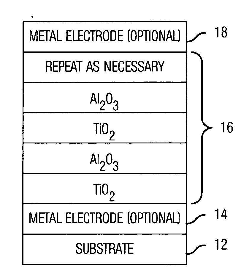
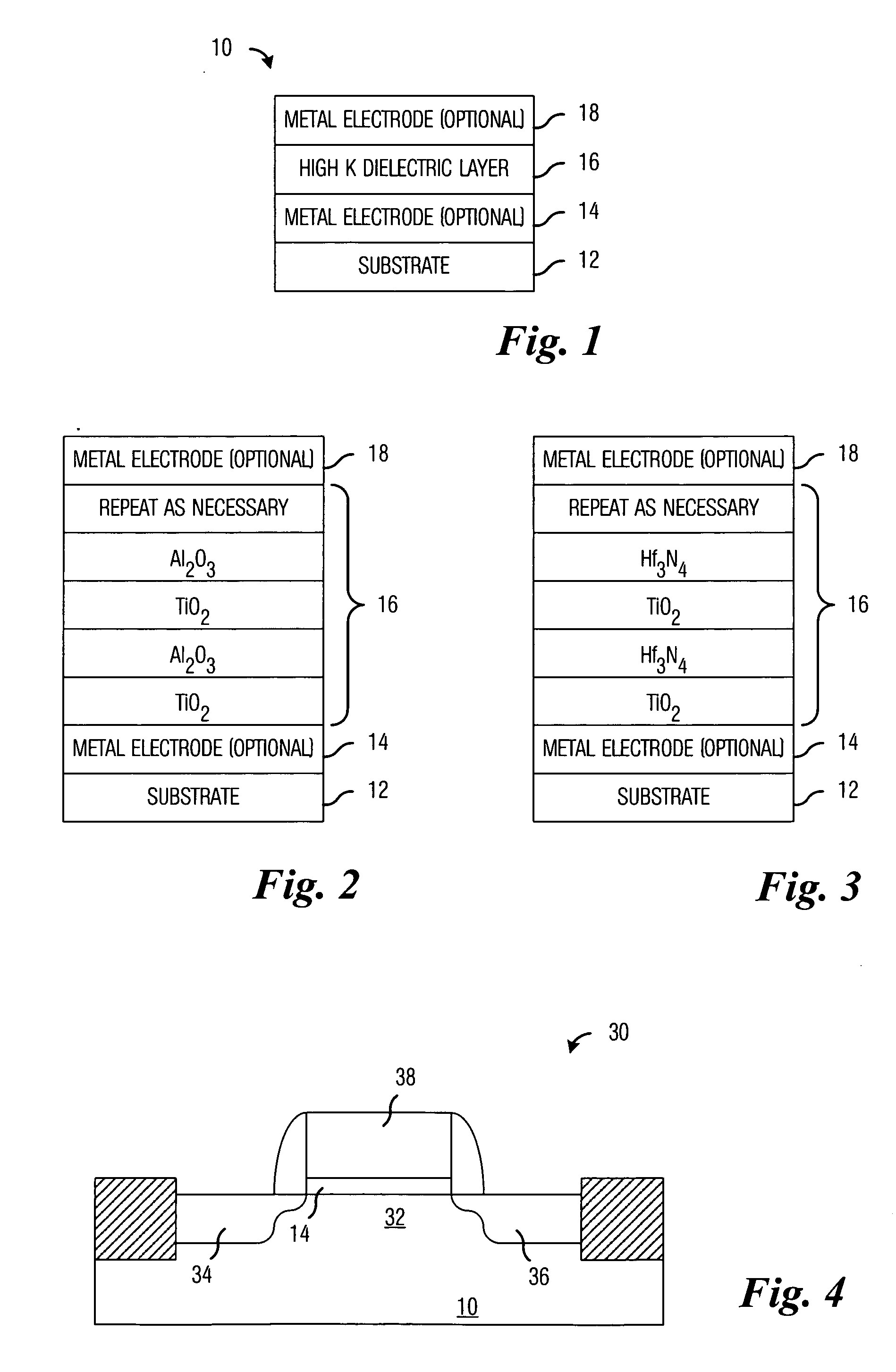
- The development of dielectric layers with a dielectric constant greater than 25, using material systems such as HfTiOxNy, TiSrvOxNy, TiAlvOxNy, and HfSrvOxNy, where u, v, w, and y represent atomic proportions, and forming nanolaminate or mixed compound structures with materials like TiO2, HfO2, Al2O3, and Ta2O5 to create high-capacity capacitors with low leakage.
Semiconductor Manufacturing Standards and Compliance
The semiconductor industry operates under stringent manufacturing standards that directly impact the development and production of silicon capacitors with enhanced dielectric constants. International standards organizations such as JEDEC, SEMI, and IEC establish comprehensive guidelines governing material specifications, process parameters, and quality metrics for advanced semiconductor devices. These standards ensure consistency across global manufacturing facilities while maintaining the precision required for next-generation computing applications.
Manufacturing compliance for silicon capacitors involves adherence to multiple regulatory frameworks, including ISO 9001 quality management systems and ISO 14001 environmental standards. The fabrication of high-dielectric-constant capacitors must comply with JEDEC standards for electrical testing, thermal cycling, and reliability assessment. Additionally, RoHS and REACH regulations impose restrictions on hazardous materials, influencing the selection of dielectric materials and dopants used in capacitor structures.
Process control standards play a critical role in achieving consistent dielectric properties across wafer lots. Statistical process control methodologies, as outlined in SEMI standards, require real-time monitoring of deposition parameters, annealing temperatures, and film thickness uniformity. Manufacturing facilities must implement advanced metrology systems capable of measuring dielectric constant variations within specified tolerances, typically requiring measurement precision better than 1% across 300mm wafers.
Quality assurance protocols for high-dielectric silicon capacitors encompass comprehensive electrical characterization, including capacitance-voltage measurements, leakage current testing, and breakdown voltage assessment. These protocols must align with JEDEC JESD standards for capacitor reliability testing, ensuring long-term stability under operational stress conditions. Traceability requirements mandate detailed documentation of material sources, process parameters, and test results throughout the manufacturing lifecycle.
Emerging compliance challenges arise from the integration of novel dielectric materials such as high-k oxides and ferroelectric compounds. Regulatory bodies are developing new standards to address the unique properties and potential risks associated with these advanced materials. Manufacturing facilities must adapt their quality systems to accommodate evolving compliance requirements while maintaining production efficiency and yield targets for next-generation computing devices.
Manufacturing compliance for silicon capacitors involves adherence to multiple regulatory frameworks, including ISO 9001 quality management systems and ISO 14001 environmental standards. The fabrication of high-dielectric-constant capacitors must comply with JEDEC standards for electrical testing, thermal cycling, and reliability assessment. Additionally, RoHS and REACH regulations impose restrictions on hazardous materials, influencing the selection of dielectric materials and dopants used in capacitor structures.
Process control standards play a critical role in achieving consistent dielectric properties across wafer lots. Statistical process control methodologies, as outlined in SEMI standards, require real-time monitoring of deposition parameters, annealing temperatures, and film thickness uniformity. Manufacturing facilities must implement advanced metrology systems capable of measuring dielectric constant variations within specified tolerances, typically requiring measurement precision better than 1% across 300mm wafers.
Quality assurance protocols for high-dielectric silicon capacitors encompass comprehensive electrical characterization, including capacitance-voltage measurements, leakage current testing, and breakdown voltage assessment. These protocols must align with JEDEC JESD standards for capacitor reliability testing, ensuring long-term stability under operational stress conditions. Traceability requirements mandate detailed documentation of material sources, process parameters, and test results throughout the manufacturing lifecycle.
Emerging compliance challenges arise from the integration of novel dielectric materials such as high-k oxides and ferroelectric compounds. Regulatory bodies are developing new standards to address the unique properties and potential risks associated with these advanced materials. Manufacturing facilities must adapt their quality systems to accommodate evolving compliance requirements while maintaining production efficiency and yield targets for next-generation computing devices.
Environmental Impact of Advanced Dielectric Processing
The manufacturing of advanced dielectric materials for silicon capacitors presents significant environmental challenges that require comprehensive assessment and mitigation strategies. Traditional dielectric processing involves high-temperature deposition techniques, chemical vapor deposition, and plasma-enhanced processes that consume substantial energy resources. These manufacturing steps typically operate at temperatures exceeding 400°C, resulting in considerable carbon footprint and energy consumption per wafer processed.
Chemical precursors used in dielectric film formation pose environmental concerns through their production, handling, and disposal phases. High-k dielectric materials often require rare earth elements and specialized compounds such as hafnium-based precursors, tantalum pentoxide, and various metal-organic frameworks. The extraction and purification of these materials generate significant environmental impact through mining operations and chemical processing facilities.
Waste stream management represents a critical environmental consideration in advanced dielectric processing. Etching and cleaning processes generate fluorinated compounds, organic solvents, and metal-containing waste streams that require specialized treatment before disposal. The semiconductor industry has implemented closed-loop recycling systems for certain chemicals, yet complete waste elimination remains challenging due to contamination and degradation of process chemicals during manufacturing cycles.
Water consumption and treatment constitute major environmental factors in dielectric processing facilities. Ultra-pure water requirements for cleaning and rinsing operations can exceed 2000 gallons per wafer in advanced nodes. Additionally, the treatment of process wastewater containing trace metals and organic compounds requires sophisticated filtration and chemical treatment systems that consume additional energy and generate secondary waste streams.
Atmospheric emissions from dielectric processing include greenhouse gases, volatile organic compounds, and particulate matter from plasma processes. Advanced abatement systems have been implemented to reduce these emissions, including thermal oxidizers and scrubber systems, though these solutions require additional energy input and periodic maintenance that generates secondary environmental impacts.
Emerging sustainable approaches focus on developing low-temperature processing techniques, alternative precursor chemistries with reduced environmental impact, and improved process efficiency to minimize waste generation. Green chemistry principles are being integrated into dielectric material development to reduce reliance on hazardous substances while maintaining performance requirements for advanced computing applications.
Chemical precursors used in dielectric film formation pose environmental concerns through their production, handling, and disposal phases. High-k dielectric materials often require rare earth elements and specialized compounds such as hafnium-based precursors, tantalum pentoxide, and various metal-organic frameworks. The extraction and purification of these materials generate significant environmental impact through mining operations and chemical processing facilities.
Waste stream management represents a critical environmental consideration in advanced dielectric processing. Etching and cleaning processes generate fluorinated compounds, organic solvents, and metal-containing waste streams that require specialized treatment before disposal. The semiconductor industry has implemented closed-loop recycling systems for certain chemicals, yet complete waste elimination remains challenging due to contamination and degradation of process chemicals during manufacturing cycles.
Water consumption and treatment constitute major environmental factors in dielectric processing facilities. Ultra-pure water requirements for cleaning and rinsing operations can exceed 2000 gallons per wafer in advanced nodes. Additionally, the treatment of process wastewater containing trace metals and organic compounds requires sophisticated filtration and chemical treatment systems that consume additional energy and generate secondary waste streams.
Atmospheric emissions from dielectric processing include greenhouse gases, volatile organic compounds, and particulate matter from plasma processes. Advanced abatement systems have been implemented to reduce these emissions, including thermal oxidizers and scrubber systems, though these solutions require additional energy input and periodic maintenance that generates secondary environmental impacts.
Emerging sustainable approaches focus on developing low-temperature processing techniques, alternative precursor chemistries with reduced environmental impact, and improved process efficiency to minimize waste generation. Green chemistry principles are being integrated into dielectric material development to reduce reliance on hazardous substances while maintaining performance requirements for advanced computing applications.
Unlock deeper insights with PatSnap Eureka Quick Research — get a full tech report to explore trends and direct your research. Try now!
Generate Your Research Report Instantly with AI Agent
Supercharge your innovation with PatSnap Eureka AI Agent Platform!