

Improving Photon Avalanche Diodes for High-Bandwidth Wireless Communication
MAY 15, 20269 MIN READ
Generate Your Research Report Instantly with AI Agent
PatSnap Eureka helps you evaluate technical feasibility & market potential.
Photon Avalanche Diode Development Background and Objectives
Photon Avalanche Diodes (PADs) represent a critical advancement in photodetection technology, emerging from the fundamental need to overcome the limitations of conventional photodiodes in high-speed optical communication systems. The development of PADs traces back to the early understanding of avalanche multiplication phenomena in semiconductor materials, where impact ionization creates cascading electron-hole pairs, dramatically amplifying photocurrent signals.
The evolution of PAD technology has been driven by the exponential growth in data transmission demands across telecommunications, data centers, and emerging applications such as quantum communication and LiDAR systems. Traditional photodiodes face inherent bandwidth limitations due to transit time effects and capacitive loading, creating bottlenecks in high-frequency optical signal detection. PADs address these constraints through their unique avalanche multiplication mechanism, enabling enhanced sensitivity while maintaining high-speed operation.
Current technological trends indicate a shift toward ultra-high bandwidth wireless communication systems operating at frequencies exceeding 100 GHz, necessitating photodetectors capable of matching these performance requirements. The integration of 5G and future 6G networks, along with satellite communication systems, demands photodetection solutions that can handle increasingly complex modulation schemes and higher data rates while maintaining signal integrity.
The primary objective of advancing PAD technology centers on achieving optimal balance between gain, bandwidth, and noise characteristics. Key performance targets include extending operational bandwidth beyond 50 GHz while maintaining avalanche gain factors of 10-20 dB, reducing excess noise factors below 3 dB, and improving temperature stability across industrial operating ranges. Additionally, the development aims to enhance manufacturing reproducibility and reduce production costs to enable widespread commercial adoption.
Secondary objectives encompass improving device reliability under high-power optical inputs, developing novel semiconductor material systems such as InGaAs and AlInAs heterostructures, and implementing advanced device architectures including separate absorption and multiplication regions. These enhancements target specific applications in coherent optical communication systems, where phase and amplitude information preservation is critical for advanced modulation formats.
The evolution of PAD technology has been driven by the exponential growth in data transmission demands across telecommunications, data centers, and emerging applications such as quantum communication and LiDAR systems. Traditional photodiodes face inherent bandwidth limitations due to transit time effects and capacitive loading, creating bottlenecks in high-frequency optical signal detection. PADs address these constraints through their unique avalanche multiplication mechanism, enabling enhanced sensitivity while maintaining high-speed operation.
Current technological trends indicate a shift toward ultra-high bandwidth wireless communication systems operating at frequencies exceeding 100 GHz, necessitating photodetectors capable of matching these performance requirements. The integration of 5G and future 6G networks, along with satellite communication systems, demands photodetection solutions that can handle increasingly complex modulation schemes and higher data rates while maintaining signal integrity.
The primary objective of advancing PAD technology centers on achieving optimal balance between gain, bandwidth, and noise characteristics. Key performance targets include extending operational bandwidth beyond 50 GHz while maintaining avalanche gain factors of 10-20 dB, reducing excess noise factors below 3 dB, and improving temperature stability across industrial operating ranges. Additionally, the development aims to enhance manufacturing reproducibility and reduce production costs to enable widespread commercial adoption.
Secondary objectives encompass improving device reliability under high-power optical inputs, developing novel semiconductor material systems such as InGaAs and AlInAs heterostructures, and implementing advanced device architectures including separate absorption and multiplication regions. These enhancements target specific applications in coherent optical communication systems, where phase and amplitude information preservation is critical for advanced modulation formats.
Market Demand for High-Bandwidth Wireless Communication Systems
The global wireless communication market is experiencing unprecedented growth driven by the exponential increase in data consumption and the proliferation of connected devices. Mobile data traffic continues to surge as consumers demand higher quality video streaming, real-time gaming, and immersive augmented reality experiences. This trend has created an urgent need for communication systems capable of delivering significantly higher bandwidth than current technologies can provide.
Fifth-generation wireless networks represent a critical stepping stone, but emerging applications are already pushing beyond their capabilities. Ultra-high-definition video content, virtual reality applications, and industrial Internet of Things deployments require data transmission rates that strain existing infrastructure. The telecommunications industry recognizes that future networks must support terabit-per-second data rates to accommodate these evolving demands.
Enterprise markets are driving substantial demand for high-bandwidth wireless solutions. Data centers require ultra-fast interconnects for cloud computing and artificial intelligence workloads. Financial institutions need low-latency, high-capacity links for algorithmic trading systems. Manufacturing facilities are implementing Industry 4.0 initiatives that depend on real-time data exchange between automated systems and control centers.
The aerospace and defense sectors present specialized market opportunities for advanced wireless communication systems. Satellite communication networks require components capable of handling massive data throughput while operating in harsh environmental conditions. Military applications demand secure, high-bandwidth communication links that can function reliably in contested electromagnetic environments.
Consumer electronics manufacturers are incorporating increasingly sophisticated wireless capabilities into their products. Smart home ecosystems, autonomous vehicles, and wearable devices all contribute to the growing demand for wireless infrastructure that can support multiple high-bandwidth connections simultaneously. The convergence of these technologies is creating market pressure for communication systems that can deliver consistent performance across diverse application scenarios.
Photon avalanche diodes represent a promising solution to address these bandwidth limitations. Their superior sensitivity and speed characteristics make them particularly well-suited for optical communication systems that can meet the stringent performance requirements of next-generation wireless networks. The market opportunity for improved photon avalanche diode technology extends across telecommunications infrastructure, enterprise networking equipment, and specialized communication systems serving critical applications in aerospace, defense, and industrial automation sectors.
Fifth-generation wireless networks represent a critical stepping stone, but emerging applications are already pushing beyond their capabilities. Ultra-high-definition video content, virtual reality applications, and industrial Internet of Things deployments require data transmission rates that strain existing infrastructure. The telecommunications industry recognizes that future networks must support terabit-per-second data rates to accommodate these evolving demands.
Enterprise markets are driving substantial demand for high-bandwidth wireless solutions. Data centers require ultra-fast interconnects for cloud computing and artificial intelligence workloads. Financial institutions need low-latency, high-capacity links for algorithmic trading systems. Manufacturing facilities are implementing Industry 4.0 initiatives that depend on real-time data exchange between automated systems and control centers.
The aerospace and defense sectors present specialized market opportunities for advanced wireless communication systems. Satellite communication networks require components capable of handling massive data throughput while operating in harsh environmental conditions. Military applications demand secure, high-bandwidth communication links that can function reliably in contested electromagnetic environments.
Consumer electronics manufacturers are incorporating increasingly sophisticated wireless capabilities into their products. Smart home ecosystems, autonomous vehicles, and wearable devices all contribute to the growing demand for wireless infrastructure that can support multiple high-bandwidth connections simultaneously. The convergence of these technologies is creating market pressure for communication systems that can deliver consistent performance across diverse application scenarios.
Photon avalanche diodes represent a promising solution to address these bandwidth limitations. Their superior sensitivity and speed characteristics make them particularly well-suited for optical communication systems that can meet the stringent performance requirements of next-generation wireless networks. The market opportunity for improved photon avalanche diode technology extends across telecommunications infrastructure, enterprise networking equipment, and specialized communication systems serving critical applications in aerospace, defense, and industrial automation sectors.
Current PAD Performance Limitations and Technical Challenges
Photon Avalanche Diodes face significant performance limitations that constrain their effectiveness in high-bandwidth wireless communication applications. The primary challenge lies in achieving optimal balance between sensitivity, speed, and noise characteristics. Current PAD devices exhibit limited bandwidth capabilities, typically operating below 10 GHz, which restricts their utility in next-generation wireless systems requiring multi-gigabit data transmission rates.
Dark current represents a critical performance bottleneck in contemporary PAD implementations. Excessive dark current generation leads to elevated noise floors, reducing signal-to-noise ratios and compromising detection sensitivity. This phenomenon becomes particularly pronounced at elevated operating temperatures, limiting deployment scenarios and requiring complex thermal management solutions that increase system complexity and power consumption.
Timing jitter constitutes another fundamental limitation affecting PAD performance in high-speed applications. Current devices demonstrate timing uncertainties in the picosecond range, which directly impacts the precision of optical pulse detection and limits achievable data rates. This jitter originates from statistical variations in the avalanche multiplication process and carrier transit time fluctuations within the device structure.
Manufacturing consistency presents substantial challenges for widespread PAD adoption. Existing fabrication processes struggle to maintain uniform device characteristics across production batches, resulting in significant performance variations. These inconsistencies affect key parameters including breakdown voltage, multiplication gain, and spectral response, complicating system design and integration efforts.
Temperature sensitivity remains a persistent technical obstacle. PAD performance characteristics exhibit strong temperature dependencies, particularly regarding breakdown voltage and multiplication gain stability. Operating temperature variations cause significant parameter drift, necessitating complex compensation circuits and limiting operational temperature ranges for reliable performance.
Spectral response optimization presents ongoing challenges for broadband wireless applications. Current PAD designs often exhibit limited spectral coverage or non-uniform responsivity across desired wavelength ranges. This limitation restricts their effectiveness in wavelength-division multiplexing systems and multi-channel communication architectures.
Power consumption and heat dissiperation issues further constrain PAD implementation in portable and battery-powered wireless devices. High operating voltages required for avalanche multiplication, combined with substantial bias currents, result in significant power requirements that conflict with energy efficiency demands in modern communication systems.
Integration complexity with complementary metal-oxide-semiconductor processes poses additional technical hurdles. Current PAD structures often require specialized fabrication steps incompatible with standard semiconductor manufacturing workflows, increasing production costs and limiting scalability for mass-market applications.
Dark current represents a critical performance bottleneck in contemporary PAD implementations. Excessive dark current generation leads to elevated noise floors, reducing signal-to-noise ratios and compromising detection sensitivity. This phenomenon becomes particularly pronounced at elevated operating temperatures, limiting deployment scenarios and requiring complex thermal management solutions that increase system complexity and power consumption.
Timing jitter constitutes another fundamental limitation affecting PAD performance in high-speed applications. Current devices demonstrate timing uncertainties in the picosecond range, which directly impacts the precision of optical pulse detection and limits achievable data rates. This jitter originates from statistical variations in the avalanche multiplication process and carrier transit time fluctuations within the device structure.
Manufacturing consistency presents substantial challenges for widespread PAD adoption. Existing fabrication processes struggle to maintain uniform device characteristics across production batches, resulting in significant performance variations. These inconsistencies affect key parameters including breakdown voltage, multiplication gain, and spectral response, complicating system design and integration efforts.
Temperature sensitivity remains a persistent technical obstacle. PAD performance characteristics exhibit strong temperature dependencies, particularly regarding breakdown voltage and multiplication gain stability. Operating temperature variations cause significant parameter drift, necessitating complex compensation circuits and limiting operational temperature ranges for reliable performance.
Spectral response optimization presents ongoing challenges for broadband wireless applications. Current PAD designs often exhibit limited spectral coverage or non-uniform responsivity across desired wavelength ranges. This limitation restricts their effectiveness in wavelength-division multiplexing systems and multi-channel communication architectures.
Power consumption and heat dissiperation issues further constrain PAD implementation in portable and battery-powered wireless devices. High operating voltages required for avalanche multiplication, combined with substantial bias currents, result in significant power requirements that conflict with energy efficiency demands in modern communication systems.
Integration complexity with complementary metal-oxide-semiconductor processes poses additional technical hurdles. Current PAD structures often require specialized fabrication steps incompatible with standard semiconductor manufacturing workflows, increasing production costs and limiting scalability for mass-market applications.
Existing PAD Enhancement Solutions for Wireless Applications
01 High-speed avalanche photodiode structures for enhanced bandwidth
Advanced photodiode structures are designed with optimized doping profiles and geometric configurations to achieve higher bandwidth performance. These structures incorporate specific layer arrangements and material compositions that enable faster carrier transit times and reduced capacitance, resulting in improved frequency response characteristics for high-speed optical communication applications.- High-speed avalanche photodiode structures for enhanced bandwidth: Advanced photodiode structures are designed with optimized doping profiles and geometric configurations to achieve higher bandwidth performance. These structures incorporate specific layer arrangements and material compositions that enable faster carrier transit times and reduced capacitance, resulting in improved frequency response characteristics for high-speed optical communication applications.
- Bandwidth optimization through device fabrication techniques: Manufacturing processes and fabrication methods are employed to enhance the bandwidth characteristics of avalanche photodiodes. These techniques involve precise control of semiconductor processing parameters, including ion implantation, diffusion processes, and epitaxial growth conditions to minimize parasitic effects and maximize operational frequency ranges.
- Circuit integration and packaging for bandwidth enhancement: Integration of avalanche photodiodes with specialized circuitry and advanced packaging solutions to improve overall system bandwidth. This approach focuses on minimizing parasitic inductances and capacitances through optimized interconnect designs, substrate materials, and thermal management strategies that maintain high-frequency performance.
- Material engineering for improved frequency response: Development of novel semiconductor materials and heterostructures specifically engineered to enhance the bandwidth capabilities of avalanche photodiodes. These materials exhibit superior carrier mobility, reduced noise characteristics, and optimized absorption properties that contribute to extended operational frequency ranges and improved signal integrity.
- Signal processing and amplification techniques for bandwidth extension: Implementation of advanced signal processing algorithms and amplification circuits designed to extend the effective bandwidth of avalanche photodiode systems. These techniques include equalization methods, noise reduction algorithms, and adaptive filtering approaches that compensate for bandwidth limitations and enhance overall system performance in high-frequency applications.
02 Circuit design and amplification techniques for bandwidth optimization
Specialized circuit topologies and amplification methods are employed to maximize the bandwidth of avalanche photodiode systems. These techniques include transimpedance amplifier designs, feedback control circuits, and signal processing methods that compensate for parasitic effects and enhance the overall system bandwidth while maintaining signal integrity and noise performance.Expand Specific Solutions03 Material engineering and fabrication processes for improved frequency response
Novel semiconductor materials and advanced fabrication techniques are utilized to create avalanche photodiodes with superior bandwidth characteristics. These approaches involve the use of specific compound semiconductors, epitaxial growth methods, and processing technologies that optimize the device physics for high-frequency operation and minimize bandwidth-limiting factors.Expand Specific Solutions04 Temperature compensation and stability enhancement methods
Temperature control and compensation techniques are implemented to maintain consistent bandwidth performance across varying operating conditions. These methods include thermal management systems, bias control circuits, and material selection strategies that minimize temperature-dependent variations in device characteristics and ensure stable high-frequency operation.Expand Specific Solutions05 Array configurations and packaging solutions for bandwidth preservation
Multi-element array designs and advanced packaging technologies are developed to maintain high bandwidth performance in complex photodiode systems. These solutions address parasitic effects, crosstalk, and interconnection challenges while preserving the individual device bandwidth characteristics in array configurations for applications requiring multiple detection channels.Expand Specific Solutions
Key Players in PAD and Optical Communication Industry
The photon avalanche diode technology for high-bandwidth wireless communication represents a rapidly evolving sector in the mature optical communications industry. The market demonstrates significant growth potential driven by increasing demand for high-speed data transmission and 5G/6G infrastructure deployment. Technology maturity varies considerably among key players, with established telecommunications giants like Huawei Technologies, NTT Inc., and Mitsubishi Electric leading in commercial deployment and manufacturing scale. Defense contractors including Raytheon and Thales SA contribute advanced sensing capabilities, while specialized optical component manufacturers such as Viavi Solutions and Ciena Corp. focus on precision engineering solutions. Research institutions like CEA and National Central University drive fundamental innovation, though commercial readiness remains heterogeneous across the competitive landscape, indicating an industry transitioning from research-intensive development toward broader market adoption.
Huawei Technologies Co., Ltd.
Technical Solution: Huawei has developed advanced photon avalanche diode (PAD) technology integrated with their optical communication systems for high-bandwidth wireless applications. Their approach focuses on silicon-based avalanche photodiodes with enhanced multiplication gain and reduced noise characteristics. The company has implemented novel guard ring structures and optimized doping profiles to achieve breakdown voltages suitable for high-speed detection in the 1.3-1.55μm wavelength range. Their PAD designs incorporate temperature compensation mechanisms and advanced packaging techniques to maintain stable performance across varying environmental conditions, enabling reliable operation in 5G and beyond wireless infrastructure applications.
Strengths: Strong integration capabilities with existing telecom infrastructure, extensive R&D resources, proven track record in optical communications. Weaknesses: Limited access to some advanced semiconductor fabrication technologies due to trade restrictions.
Koninklijke Philips NV
Technical Solution: Philips has developed photon avalanche diode technology primarily focused on medical imaging and sensing applications, with recent extensions into high-bandwidth communication systems. Their approach utilizes silicon photomultiplier (SiPM) arrays based on avalanche photodiode pixels operating in Geiger mode. The technology features low-voltage operation, high photon detection efficiency, and excellent timing resolution. For wireless communication applications, Philips has adapted their PAD technology to support visible light communication (VLC) systems and short-range optical wireless links, incorporating advanced signal processing algorithms to optimize bandwidth utilization and minimize inter-symbol interference in high-speed data transmission scenarios.
Strengths: Strong expertise in photon detection technology, established manufacturing infrastructure, proven reliability in medical applications. Weaknesses: Limited focus on telecommunications market, less specialized in long-range wireless communication requirements.
Core Innovations in High-Performance Avalanche Photodiodes
Avalanche Photodiode
PatentInactiveUS20090315073A1
Innovation
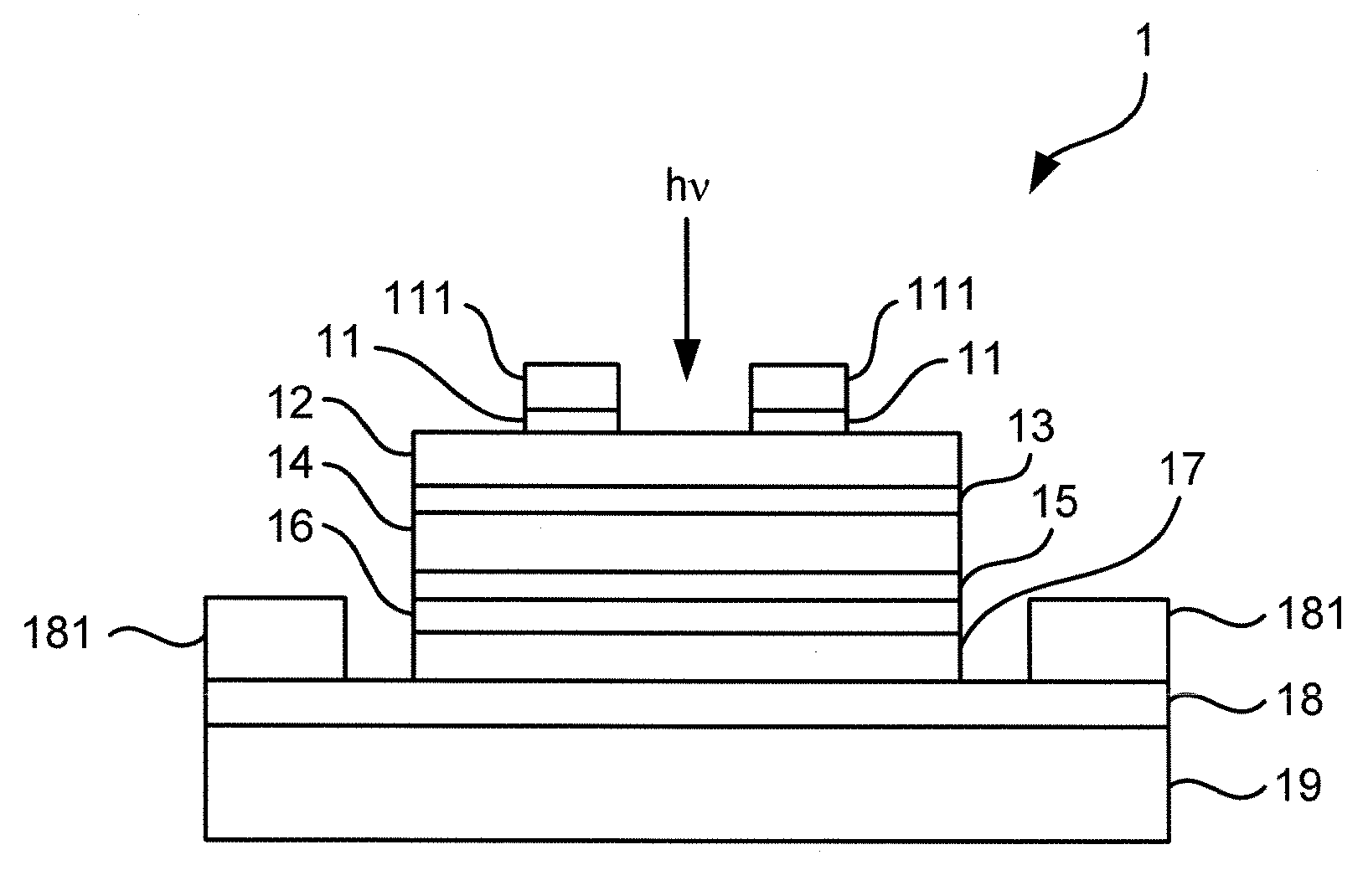
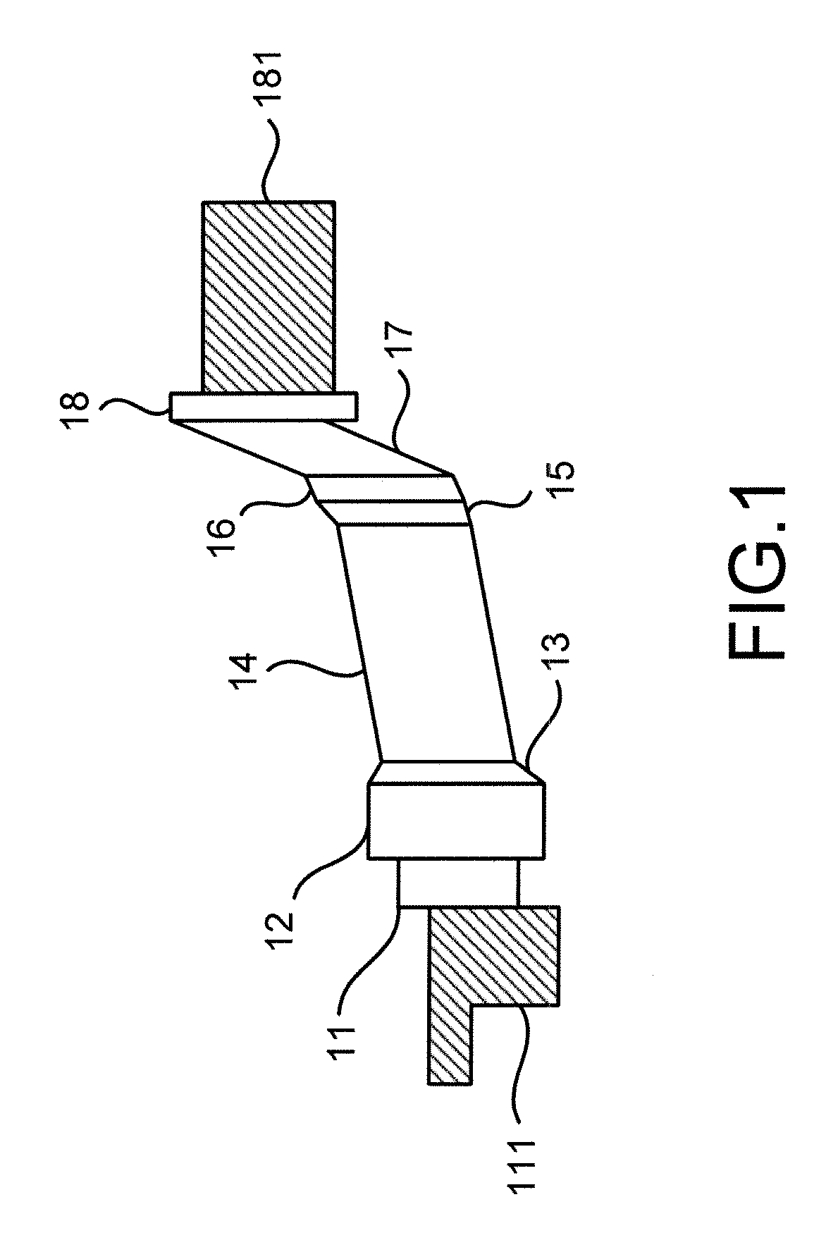
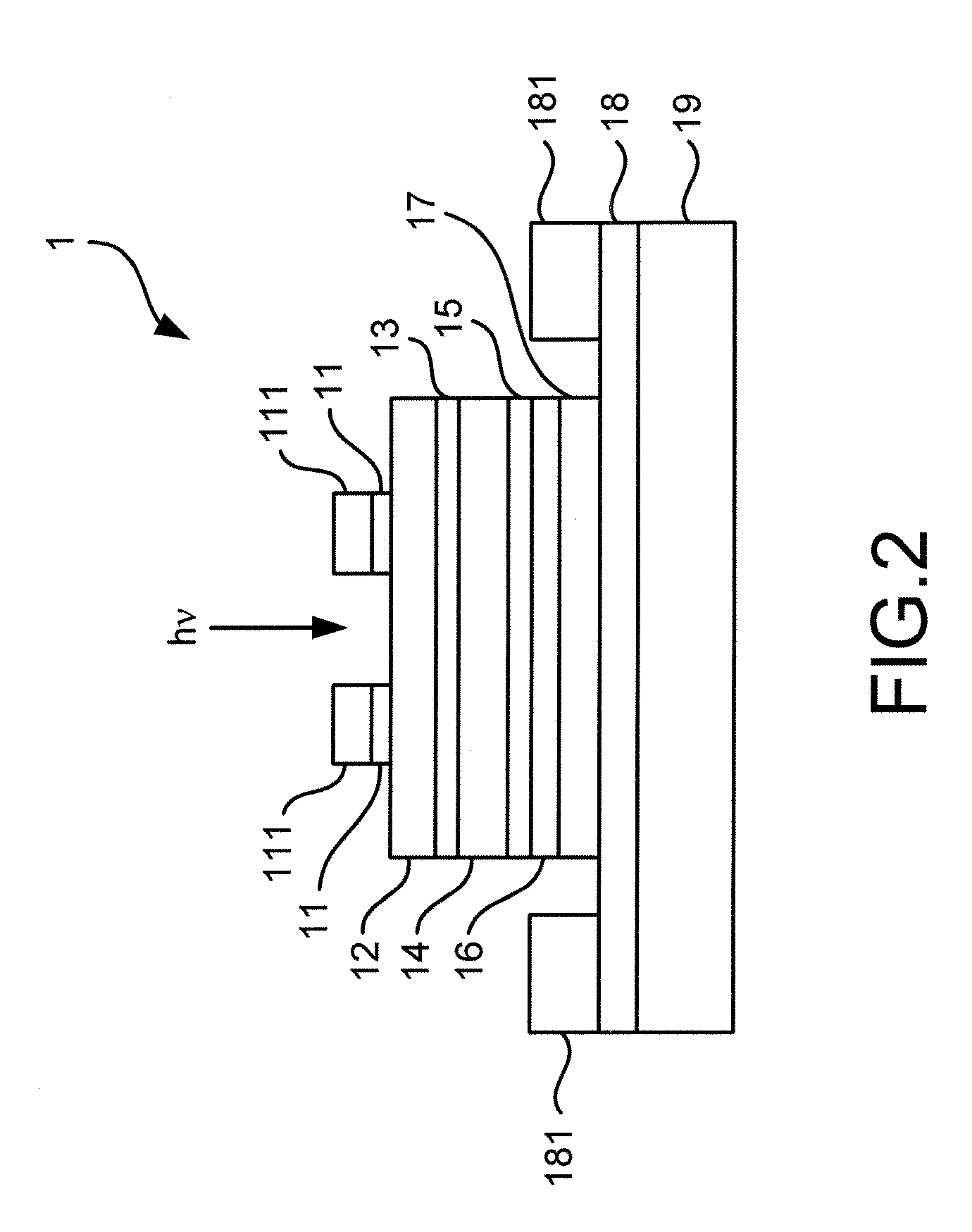
- The avalanche photodiode structure is modified to an n-i-n-i-p epitaxial structure with an InP transport layer above the absorption layer, concentrating the electric field on the multiplication layer for avalanche production and a minor part on the absorption layer for carrier transfer, reducing capacitance and carrier transferring time.

Improvements in avalanche photo-diodes
PatentInactiveEP1142029B1
Innovation
- An avalanche photo-diode arrangement with at least two reverse-biased photo-diodes subjected to an oscillating voltage with a period between 4 and 32 times the avalanche zone transit time, allowing discrimination against dark counts and reducing noise through phase-aligned operation and optimized oscillation periods.


Spectrum Allocation and Regulatory Framework for Optical Wireless
The deployment of photon avalanche diodes in high-bandwidth wireless communication systems operates within a complex regulatory landscape that governs optical wireless spectrum allocation. Unlike traditional radio frequency communications, optical wireless systems utilizing wavelengths in the infrared and near-infrared spectrum face unique regulatory considerations that vary significantly across global jurisdictions.
Current spectrum allocation frameworks for optical wireless communications primarily focus on eye safety regulations rather than interference management. The International Electrotechnical Commission (IEC) 60825 standard serves as the foundation for laser safety classifications, directly impacting the permissible power levels for photon avalanche diode-based systems. These safety constraints establish maximum allowable exposure limits that influence system design parameters, particularly for outdoor free-space optical links where higher power densities may be required for reliable communication.
The Federal Communications Commission in the United States and similar regulatory bodies worldwide have established specific guidelines for optical communication devices operating in unlicensed spectrum bands. The 1550nm wavelength region, commonly used with InGaAs-based photon avalanche diodes, benefits from relaxed eye safety requirements due to atmospheric absorption characteristics, enabling higher power transmission levels compared to visible or near-infrared wavelengths.
International Telecommunication Union recommendations, particularly ITU-R F.2106, provide technical and operational guidelines for terrestrial free-space optical links. These recommendations address coordination procedures, interference mitigation strategies, and deployment considerations that directly impact photon avalanche diode system implementations. The regulatory framework emphasizes the need for adaptive power control mechanisms and beam steering capabilities to minimize potential interference with other optical systems.
Emerging regulatory trends indicate increasing recognition of optical wireless communications as a viable solution for spectrum congestion relief. Recent developments in regulatory frameworks show movement toward establishing dedicated optical wireless communication bands and simplified licensing procedures for high-frequency optical links. These evolving regulations are particularly relevant for photon avalanche diode applications in urban environments where traditional RF spectrum is heavily congested.
The regulatory landscape also encompasses environmental and operational considerations specific to optical wireless deployments. Weather-related attenuation, building codes for rooftop installations, and aviation safety requirements create additional compliance layers that influence system architecture decisions. These factors necessitate robust link budget calculations and redundancy mechanisms in photon avalanche diode-based communication systems to maintain regulatory compliance while achieving desired performance metrics.
Current spectrum allocation frameworks for optical wireless communications primarily focus on eye safety regulations rather than interference management. The International Electrotechnical Commission (IEC) 60825 standard serves as the foundation for laser safety classifications, directly impacting the permissible power levels for photon avalanche diode-based systems. These safety constraints establish maximum allowable exposure limits that influence system design parameters, particularly for outdoor free-space optical links where higher power densities may be required for reliable communication.
The Federal Communications Commission in the United States and similar regulatory bodies worldwide have established specific guidelines for optical communication devices operating in unlicensed spectrum bands. The 1550nm wavelength region, commonly used with InGaAs-based photon avalanche diodes, benefits from relaxed eye safety requirements due to atmospheric absorption characteristics, enabling higher power transmission levels compared to visible or near-infrared wavelengths.
International Telecommunication Union recommendations, particularly ITU-R F.2106, provide technical and operational guidelines for terrestrial free-space optical links. These recommendations address coordination procedures, interference mitigation strategies, and deployment considerations that directly impact photon avalanche diode system implementations. The regulatory framework emphasizes the need for adaptive power control mechanisms and beam steering capabilities to minimize potential interference with other optical systems.
Emerging regulatory trends indicate increasing recognition of optical wireless communications as a viable solution for spectrum congestion relief. Recent developments in regulatory frameworks show movement toward establishing dedicated optical wireless communication bands and simplified licensing procedures for high-frequency optical links. These evolving regulations are particularly relevant for photon avalanche diode applications in urban environments where traditional RF spectrum is heavily congested.
The regulatory landscape also encompasses environmental and operational considerations specific to optical wireless deployments. Weather-related attenuation, building codes for rooftop installations, and aviation safety requirements create additional compliance layers that influence system architecture decisions. These factors necessitate robust link budget calculations and redundancy mechanisms in photon avalanche diode-based communication systems to maintain regulatory compliance while achieving desired performance metrics.
Environmental Impact Assessment of PAD Manufacturing Processes
The manufacturing of Photon Avalanche Diodes for high-bandwidth wireless communication applications presents several environmental considerations that require comprehensive assessment. The semiconductor fabrication processes involved in PAD production typically consume significant amounts of energy, water, and chemical resources while generating various waste streams that must be carefully managed.
Energy consumption represents one of the most substantial environmental impacts in PAD manufacturing. The fabrication facilities require continuous operation of cleanrooms, vacuum systems, and high-temperature processing equipment. Advanced lithography processes, essential for creating the precise junction structures in PADs, demand substantial electrical power for exposure systems and environmental controls. The carbon footprint associated with this energy usage varies significantly depending on the regional electricity grid composition and the facility's adoption of renewable energy sources.
Chemical usage and waste generation constitute another critical environmental concern. PAD manufacturing involves numerous hazardous chemicals including acids, solvents, and dopant materials. Hydrofluoric acid used in etching processes, photoresist chemicals for patterning, and various cleaning solvents create toxic waste streams requiring specialized treatment and disposal. The semiconductor industry has developed sophisticated waste treatment systems, but the environmental burden remains substantial, particularly for facilities operating at scale.
Water consumption and wastewater treatment present ongoing challenges in PAD fabrication. Ultra-pure water production requires extensive purification processes, while rinse cycles and cleaning operations generate contaminated wastewater containing trace metals and chemical residues. Advanced treatment systems can recover and recycle much of this water, but the initial consumption and treatment energy requirements contribute to the overall environmental impact.
Material sourcing for PAD manufacturing raises additional sustainability concerns. The extraction and processing of semiconductor-grade silicon, along with specialized materials like indium gallium arsenide for advanced PAD structures, involve energy-intensive mining and refining operations. The geographic concentration of these materials in specific regions also creates supply chain vulnerabilities and transportation-related emissions.
Emerging manufacturing approaches show promise for reducing environmental impacts. Advanced process technologies that minimize chemical usage, improved energy efficiency in fabrication equipment, and closed-loop water recycling systems are being implemented across the industry. Additionally, the development of alternative materials and manufacturing techniques specifically for PAD applications may offer pathways to more sustainable production methods while maintaining the performance requirements for high-bandwidth wireless communication systems.
Energy consumption represents one of the most substantial environmental impacts in PAD manufacturing. The fabrication facilities require continuous operation of cleanrooms, vacuum systems, and high-temperature processing equipment. Advanced lithography processes, essential for creating the precise junction structures in PADs, demand substantial electrical power for exposure systems and environmental controls. The carbon footprint associated with this energy usage varies significantly depending on the regional electricity grid composition and the facility's adoption of renewable energy sources.
Chemical usage and waste generation constitute another critical environmental concern. PAD manufacturing involves numerous hazardous chemicals including acids, solvents, and dopant materials. Hydrofluoric acid used in etching processes, photoresist chemicals for patterning, and various cleaning solvents create toxic waste streams requiring specialized treatment and disposal. The semiconductor industry has developed sophisticated waste treatment systems, but the environmental burden remains substantial, particularly for facilities operating at scale.
Water consumption and wastewater treatment present ongoing challenges in PAD fabrication. Ultra-pure water production requires extensive purification processes, while rinse cycles and cleaning operations generate contaminated wastewater containing trace metals and chemical residues. Advanced treatment systems can recover and recycle much of this water, but the initial consumption and treatment energy requirements contribute to the overall environmental impact.
Material sourcing for PAD manufacturing raises additional sustainability concerns. The extraction and processing of semiconductor-grade silicon, along with specialized materials like indium gallium arsenide for advanced PAD structures, involve energy-intensive mining and refining operations. The geographic concentration of these materials in specific regions also creates supply chain vulnerabilities and transportation-related emissions.
Emerging manufacturing approaches show promise for reducing environmental impacts. Advanced process technologies that minimize chemical usage, improved energy efficiency in fabrication equipment, and closed-loop water recycling systems are being implemented across the industry. Additionally, the development of alternative materials and manufacturing techniques specifically for PAD applications may offer pathways to more sustainable production methods while maintaining the performance requirements for high-bandwidth wireless communication systems.
Unlock deeper insights with PatSnap Eureka Quick Research — get a full tech report to explore trends and direct your research. Try now!
Generate Your Research Report Instantly with AI Agent
Supercharge your innovation with PatSnap Eureka AI Agent Platform!