Low Temperature Sintering Application in Flexible Electronics Devices
SEP 25, 20259 MIN READ
Generate Your Research Report Instantly with AI Agent
Patsnap Eureka helps you evaluate technical feasibility & market potential.
Low Temperature Sintering Evolution and Objectives
Low temperature sintering technology has evolved significantly over the past decades, transforming from traditional high-temperature ceramic and metal processing methods to innovative approaches that enable processing at substantially lower temperatures. This evolution has been primarily driven by the growing demand for flexible electronics, which require manufacturing processes compatible with temperature-sensitive substrates such as polymers and paper.
The journey of low temperature sintering began in the 1990s with the development of nanoparticle-based metal inks, which demonstrated the size-dependent melting point depression phenomenon. This breakthrough revealed that metal nanoparticles could sinter at temperatures hundreds of degrees lower than their bulk counterparts, opening new possibilities for electronic device fabrication.
By the early 2000s, silver nanoparticle inks emerged as the first commercially viable solution, capable of sintering at temperatures around 200-300°C, significantly lower than the melting point of bulk silver (961°C). This advancement enabled the production of conductive patterns on polyimide and other high-temperature polymers, marking the first generation of flexible electronic devices.
The next significant milestone occurred around 2010 with the introduction of chemical sintering approaches, which further reduced processing temperatures to below 150°C. These methods utilized reactive agents to remove stabilizing ligands from nanoparticles, inducing sintering without substantial thermal energy input. This development expanded the range of compatible substrates to include more common polymers like PET and PEN.
Recent years have witnessed the emergence of photonic sintering techniques, particularly intense pulsed light (IPL) sintering, which enables extremely rapid processing of metal nanostructures with minimal heat transfer to underlying substrates. This approach has reduced effective processing temperatures to below 100°C while maintaining excellent electrical performance of the sintered materials.
The primary objective of current low temperature sintering research is to achieve high-performance electrical, mechanical, and thermal properties at processing temperatures below 120°C, which would make the technology compatible with virtually all polymer substrates and even paper-based materials. Additionally, researchers aim to develop environmentally friendly formulations that reduce or eliminate the use of precious metals and harmful solvents.
Another critical goal is to enhance the scalability and reliability of low temperature sintering processes for mass production environments, ensuring consistent performance across large substrate areas and high throughput manufacturing lines. This includes developing in-line quality control methods and predictive models for sintering behavior under various processing conditions.
Flexible Electronics Market Demand Analysis
The flexible electronics market has witnessed remarkable growth over the past decade, driven by increasing consumer demand for portable, lightweight, and bendable electronic devices. Current market analysis indicates that the global flexible electronics market is projected to reach $42 billion by 2027, growing at a CAGR of approximately 11% from 2022 to 2027. This substantial growth is primarily fueled by the expanding applications across multiple industries including consumer electronics, healthcare, automotive, and aerospace.
Consumer electronics represents the largest market segment, with flexible displays for smartphones, tablets, and wearable devices leading the demand. The transition from rigid to flexible form factors has been accelerated by consumer preferences for devices that offer enhanced durability, portability, and novel user experiences. Major smartphone manufacturers have already introduced foldable displays, creating a new premium category that is expected to become mainstream within the next five years.
Healthcare applications present another significant growth area, with flexible biosensors, smart patches, and implantable electronics showing tremendous potential. These devices enable continuous health monitoring and personalized healthcare solutions, addressing the growing trend toward preventive medicine and remote patient monitoring. Market research indicates that healthcare applications of flexible electronics could grow at a CAGR of 14% through 2027, outpacing the overall market growth.
The automotive industry is increasingly incorporating flexible electronics in dashboard displays, lighting systems, and sensor networks. As vehicles become more connected and autonomous, the demand for seamless integration of electronics into curved and irregular surfaces is rising. This sector is expected to represent approximately 18% of the total flexible electronics market by 2025.
Regional analysis reveals that Asia-Pacific currently dominates the market, accounting for over 40% of global demand, with South Korea, Japan, and China leading in both production and consumption. North America and Europe follow, with significant investments in R&D and growing adoption across multiple industries.
Key market challenges include high manufacturing costs and technical limitations related to durability and performance under repeated mechanical stress. The cost factor remains particularly critical for mass-market adoption, with flexible electronic components typically commanding a premium of 30-50% over their rigid counterparts. However, as low-temperature sintering and other advanced manufacturing technologies mature, production costs are expected to decrease significantly.
Consumer surveys indicate strong interest in flexible electronic products, with over 65% of respondents expressing willingness to pay a premium for devices with flexible displays or form factors. This consumer readiness, coupled with ongoing technological advancements, suggests a robust demand trajectory for the foreseeable future.
Technical Barriers in Low Temperature Sintering
Despite significant advancements in low temperature sintering technologies for flexible electronics, several critical technical barriers continue to impede widespread commercial adoption. The fundamental challenge lies in achieving reliable electrical connections while maintaining the mechanical flexibility that defines these devices. Traditional high-temperature sintering processes (>200°C) are incompatible with polymer substrates commonly used in flexible electronics, which typically degrade at temperatures above 150°C.
Material compatibility presents a significant obstacle, as the thermal expansion coefficient mismatch between conductive materials and flexible substrates often leads to delamination or cracking during thermal cycling. This becomes particularly problematic when attempting to integrate rigid components with flexible substrates using low temperature sintering techniques.
The sintering kinetics at lower temperatures (<150°C) remain insufficient for many applications, resulting in incomplete particle coalescence and compromised electrical conductivity. Current low-temperature sintering methods often yield conductivities that are 3-5 times lower than their bulk material counterparts, creating performance bottlenecks in high-frequency or high-power applications.
Process scalability represents another major barrier. Laboratory-scale demonstrations of low temperature sintering techniques frequently employ specialized equipment or time-consuming procedures that are difficult to translate to high-volume manufacturing environments. The lack of standardized processes and quality control metrics further complicates industrial implementation.
Environmental stability of low-temperature sintered connections remains problematic, with many exhibiting accelerated degradation under humidity, oxidation, or mechanical stress. This is particularly evident in silver nanoparticle-based inks, which show promising initial conductivity but may experience significant performance deterioration in operating conditions.
The cost structure of advanced low-temperature sintering materials presents economic barriers to adoption. Specialized nanoparticle inks, reactive metal formulations, and photonic sintering equipment often carry premium pricing that challenges the value proposition for mass-market flexible electronics applications.
Energy efficiency concerns persist with certain emerging techniques like photonic sintering, which may require significant power input despite operating at nominally "low temperatures." This contradicts the sustainability goals often associated with flexible electronics development.
Addressing these technical barriers requires interdisciplinary approaches combining materials science, chemical engineering, and manufacturing process optimization to develop next-generation low temperature sintering solutions that can meet the demanding requirements of flexible electronic devices.
Current Low Temperature Sintering Solutions
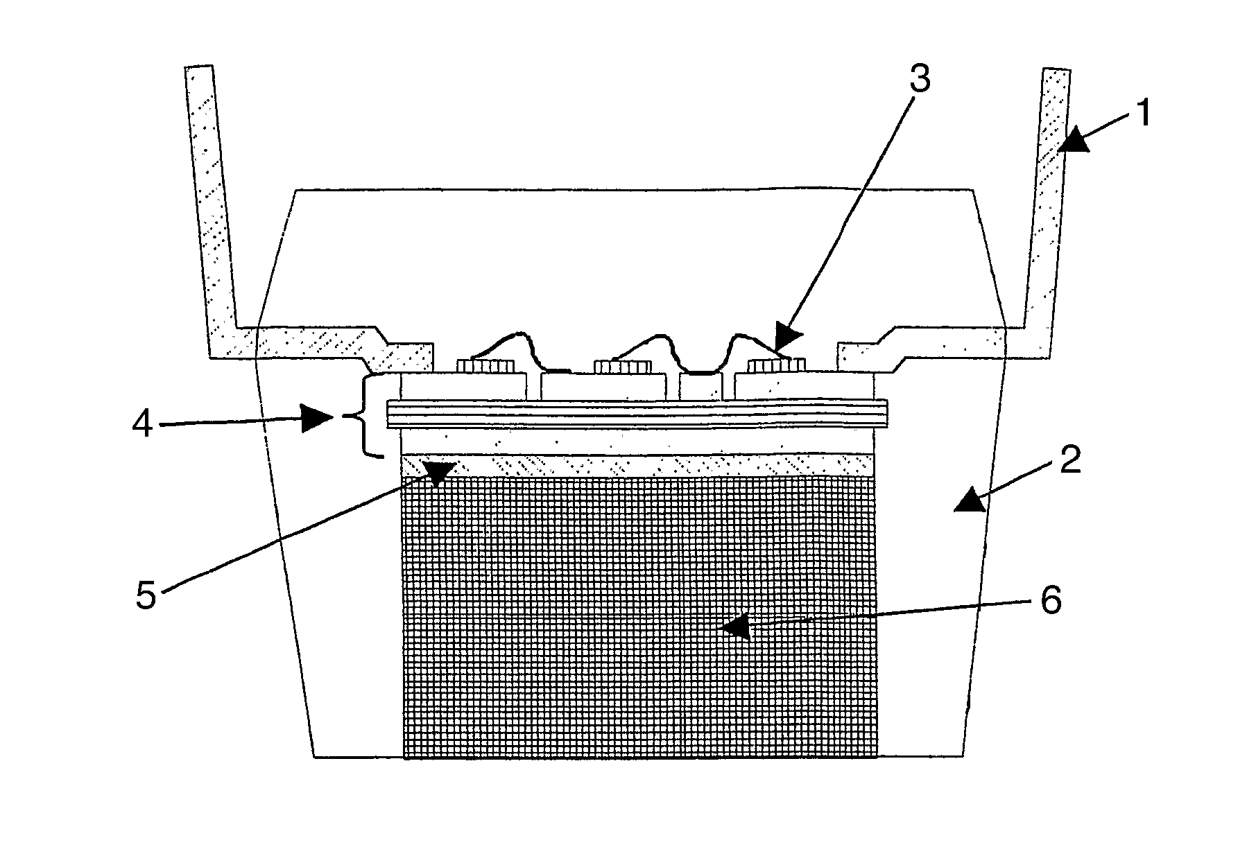
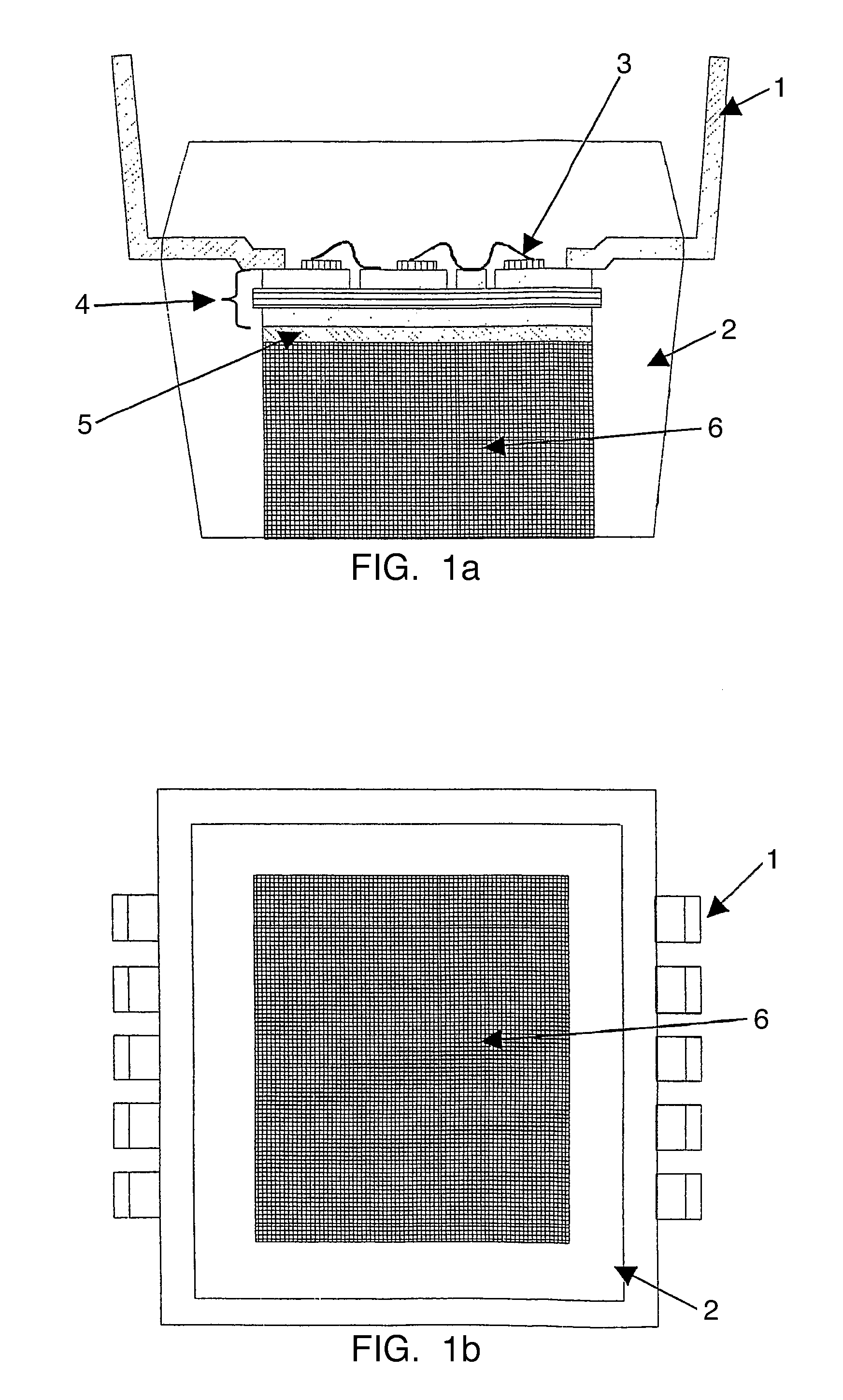
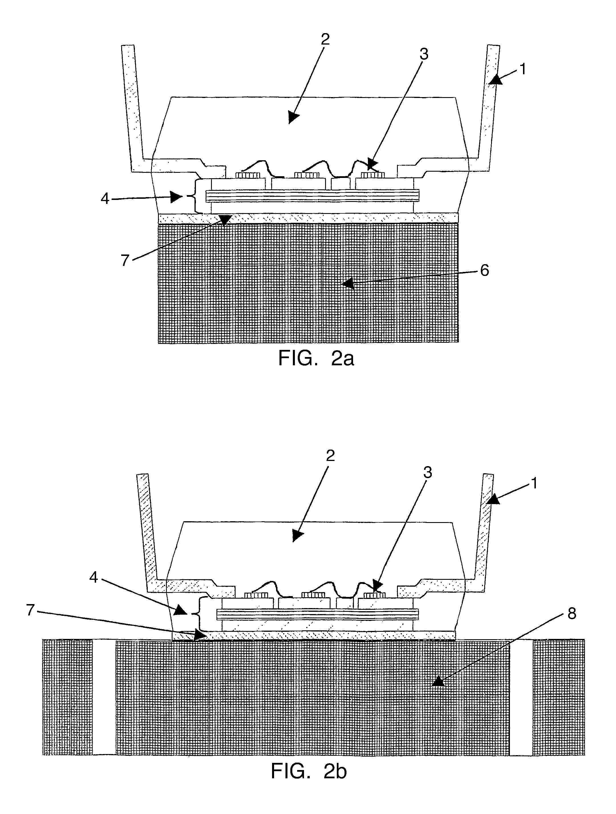
01 Low temperature sintering additives and compositions
Various additives and compositions can be used to lower the sintering temperature of ceramic materials. These include specific metal oxides, glass frits, and other compounds that act as sintering aids by forming liquid phases at lower temperatures. These additives promote densification and grain growth at reduced temperatures, making the sintering process more energy-efficient while maintaining or improving the properties of the final product.- Ceramic materials for low temperature sintering: Various ceramic compositions have been developed specifically for low temperature sintering applications. These materials include modified dielectric ceramics, glass-ceramic composites, and specialized oxide formulations that can be sintered at temperatures significantly lower than conventional ceramics. The reduced sintering temperature helps minimize energy consumption, prevents unwanted reactions between components, and enables co-firing with low-melting-point metals like silver and copper.
- Sintering additives and flux materials: The incorporation of specific additives and flux materials can substantially lower the sintering temperature of ceramic and metallic systems. These additives work by forming liquid phases at the grain boundaries, enhancing mass transport mechanisms, and promoting densification at reduced temperatures. Common additives include glass frits, boron compounds, lithium-based fluxes, and various metal oxides that create eutectic compositions with lower melting points than the primary material.
- Advanced sintering techniques for low temperature processing: Novel sintering techniques have been developed to achieve densification at lower temperatures. These include microwave sintering, spark plasma sintering, field-assisted sintering, and pressure-assisted methods. These techniques apply alternative energy sources or mechanical pressure to enhance sintering kinetics, allowing for complete densification at temperatures hundreds of degrees lower than conventional thermal processing while maintaining or improving the final material properties.
- Nanoparticle-based low temperature sintering: Utilizing nanoscale particles significantly reduces the required sintering temperature due to their high surface energy and enhanced reactivity. Nanoparticle-based sintering systems can achieve full densification at temperatures 200-400°C lower than their micron-sized counterparts. This approach is particularly valuable for electronic applications, where silver, copper, and other conductive nanoparticles can be sintered at temperatures compatible with polymer substrates and temperature-sensitive components.
- Low temperature co-fired ceramics (LTCC) technology: LTCC technology enables the integration of passive components and interconnects within a ceramic substrate that can be sintered at relatively low temperatures (typically 850-950°C). This is achieved through specialized glass-ceramic composite formulations that provide the desired electrical, mechanical, and thermal properties while maintaining compatibility with internal metal conductors. LTCC systems are widely used in high-frequency applications, sensors, and miniaturized electronic modules where integration density is critical.
02 Low temperature co-fired ceramic (LTCC) technology
LTCC technology enables the co-firing of ceramic materials and conductive metals at relatively low temperatures (typically below 900°C). This approach allows for the integration of electronic components and circuits within ceramic substrates. The process involves formulating specialized ceramic compositions that can be sintered at temperatures compatible with metals like silver and gold, while maintaining excellent electrical, mechanical, and thermal properties.Expand Specific Solutions03 Nanoparticle-assisted low temperature sintering
Utilizing nanoparticles in sintering processes can significantly reduce the required sintering temperature. Nanoscale particles have higher surface energy and reactivity compared to their bulk counterparts, which enhances diffusion and promotes densification at lower temperatures. This approach is particularly valuable for temperature-sensitive applications and can lead to energy savings while preserving the microstructure and properties of the sintered materials.Expand Specific Solutions04 Low temperature sintering for semiconductor and electronic applications
Specialized low temperature sintering techniques have been developed for semiconductor manufacturing and electronic applications. These methods enable the formation of conductive pathways, interconnects, and components without damaging temperature-sensitive substrates or materials. The processes often involve silver or copper nanoparticles, conductive pastes, or specialized bonding materials that can be sintered at temperatures compatible with polymer substrates and other heat-sensitive components.Expand Specific Solutions05 Equipment and process optimization for low temperature sintering
Advanced equipment designs and process optimizations enable effective sintering at reduced temperatures. These innovations include specialized furnaces with precise atmosphere control, microwave-assisted sintering, spark plasma sintering, and other novel heating methods. Process parameters such as heating rates, dwell times, pressure application, and cooling strategies are carefully controlled to achieve full densification at lower temperatures while maintaining desired material properties.Expand Specific Solutions
Leading Companies in Flexible Electronics Manufacturing
The low temperature sintering market in flexible electronics is in a growth phase, characterized by increasing adoption across consumer electronics, automotive, and healthcare sectors. The market is projected to expand significantly due to rising demand for lightweight, bendable devices. Technologically, the field is advancing rapidly with companies like E Ink Corp. leading in display applications, while Heraeus Precious Metals and RESONAC CORP focus on conductive materials development. Samsung Electro Mechanics and Murata Manufacturing are advancing component miniaturization, while research institutions like KIST and Fudan University are pushing boundaries in novel sintering techniques. Applied Materials and Danfoss Silicon Power are developing manufacturing equipment and power modules, creating a competitive ecosystem balancing commercial applications with fundamental research.
E Ink Corp.
Technical Solution: E Ink has developed a specialized low temperature sintering technology tailored for flexible electronic paper displays. Their approach utilizes a hybrid sintering method combining chemical and thermal processes to create conductive traces on flexible substrates at temperatures below 130°C. The company's proprietary formulation includes silver nanoparticles with surface functionalization that promotes self-sintering through ligand exchange reactions, requiring minimal thermal energy. This technology has been crucial for E Ink's development of flexible e-paper displays, where traditional high-temperature processes would damage the display materials. Their process incorporates a two-stage sintering approach: an initial chemical activation followed by a brief low-temperature thermal treatment. Research from E Ink shows their method achieves conductivity values of approximately 20% of bulk silver while maintaining compatibility with their proprietary display technologies. The company has successfully implemented this technology in commercial products including flexible e-readers and electronic shelf labels, demonstrating durability through thousands of flexing cycles without significant degradation in electrical performance.
Strengths: Specifically optimized for integration with electronic paper display technologies; minimal impact on sensitive display materials; compatible with existing manufacturing infrastructure. Weaknesses: Relatively slow processing time compared to some alternative methods; limited to specific substrate materials compatible with their display technology; moderate conductivity values compared to high-temperature processes.
Heraeus Precious Metals GmbH & Co. KG (New)
Technical Solution: Heraeus has developed advanced low temperature sintering pastes specifically engineered for flexible electronics applications. Their technology centers on metal-organic decomposition (MOD) inks containing silver carboxylates and custom-designed organic vehicles that decompose at temperatures as low as 80°C. These specialized formulations create highly conductive pathways on flexible substrates through a controlled decomposition and sintering process. Heraeus' proprietary additives promote particle coalescence at reduced temperatures while maintaining excellent adhesion to various substrate materials including PET, PEN, and TPU. The company has commercialized several product lines including Clevios™ conductive polymers and micronized silver pastes that can be processed at temperatures between 80-150°C. Their research demonstrates that these materials achieve conductivity values of 15-25% of bulk silver while maintaining flexibility through more than 10,000 bending cycles with radius as small as 3mm. Heraeus has successfully implemented this technology in applications ranging from flexible displays to medical wearables and smart packaging.
Strengths: Highly specialized formulations optimized for specific substrate types and applications; excellent adhesion properties; compatible with various deposition methods including screen printing and inkjet. Weaknesses: Higher material costs compared to conventional conductive pastes; shelf-life limitations for some formulations; requires precise process control to achieve optimal conductivity.
Key Patents in Low Temperature Sintering Technology
Method for the low-temperature pressure sintering
PatentActiveUS20110017808A1
Innovation
- The process involves pre-testing substrate units, shaping them into a robust mold module, and then connecting them to a heat sink plate using silver sintering, with a thermosetting cover compound matched to the ceramic substrate's expansion coefficient, allowing for a convex deformation and reduced mold compound usage.

Sintering device and method for electronic component
PatentActiveJP2020181907A
Innovation
- A sintering apparatus and method using silver nanopaste with high heat resistance and thermal conductivity, preheating electronic components below the melting point of the bonding material, followed by sintering at a controlled temperature and pressure, and cooling to prevent oxidation and dimensional changes.

Materials Compatibility and Sustainability Aspects
The compatibility of materials in low temperature sintering processes represents a critical factor for flexible electronics development. Traditional sintering methods often require temperatures exceeding 200°C, which limits material selection to those with high thermal stability. Low temperature sintering techniques, operating below 150°C, significantly expand the range of compatible substrate materials, including polyethylene terephthalate (PET), polyimide (PI), and even paper-based substrates that would otherwise degrade at higher temperatures.
Material interface interactions during low temperature sintering demand careful consideration. The coefficient of thermal expansion (CTE) mismatch between conductive materials and flexible substrates can lead to mechanical stress, resulting in delamination or cracking during thermal cycling. Recent advances in nanoparticle formulations with organic capping agents have improved adhesion properties while maintaining electrical performance at lower sintering temperatures.
Sustainability aspects of low temperature sintering technologies present both challenges and opportunities. The reduced energy consumption during manufacturing processes directly contributes to lower carbon footprints compared to conventional electronics fabrication. Energy savings of 30-45% have been documented when implementing low temperature sintering techniques in production environments, particularly beneficial for large-scale manufacturing operations.
Material selection for environmentally responsible flexible electronics requires consideration of end-of-life scenarios. Water-soluble and biodegradable substrates compatible with low temperature sintering are emerging as promising alternatives for transient electronics applications. These materials enable devices that can harmlessly decompose after their functional lifetime, reducing electronic waste accumulation.
The chemical composition of sintering pastes and inks presents another sustainability consideration. Traditional formulations often contain potentially harmful solvents and heavy metals. Recent research has focused on developing bio-derived alternatives and water-based systems that maintain performance while reducing environmental impact. Silver nanoparticle inks with bio-based stabilizers have demonstrated comparable conductivity to conventional formulations while significantly reducing toxicity profiles.
Recycling and material recovery processes for flexible electronics remain challenging due to the intimate integration of diverse materials. Low temperature sintering approaches that facilitate easier separation of conductive elements from substrates could enhance recyclability. Techniques such as selective dissolution and mechanical separation are being explored to improve material recovery rates from flexible electronic waste streams.
Scalability and Cost-Effectiveness Analysis
The scalability of low temperature sintering technologies represents a critical factor in their widespread adoption for flexible electronics manufacturing. Current production methods demonstrate varying degrees of scalability, with roll-to-roll (R2R) processing emerging as the most promising approach for high-volume production. R2R-compatible low temperature sintering enables continuous processing of flexible substrates, significantly increasing throughput compared to batch processing methods. However, implementation challenges remain, particularly in maintaining consistent sintering quality across large surface areas and ensuring uniform thermal distribution during the sintering process.
Cost-effectiveness analysis reveals that while initial capital investment for low temperature sintering equipment may be substantial, operational costs can be significantly lower than traditional high-temperature processes. Energy consumption reductions of 30-60% have been documented when comparing low temperature sintering to conventional thermal sintering methods. Material costs also present opportunities for savings, as lower processing temperatures enable the use of less expensive substrate materials that would otherwise degrade at higher temperatures.
Production yield represents another crucial economic factor. Current industrial implementations of low temperature sintering for flexible electronics demonstrate yield rates between 75-92%, depending on the specific technology employed. Photonic sintering technologies generally achieve higher yields than purely thermal methods, though at a higher equipment cost. The economic break-even point typically occurs at production volumes of 10,000-50,000 units, depending on device complexity and market value.
Supply chain considerations further impact scalability and cost-effectiveness. The availability of specialized conductive inks and pastes formulated specifically for low temperature sintering remains limited, with fewer suppliers than for traditional electronics materials. This supply constraint can lead to price premiums of 15-40% compared to conventional materials. However, as adoption increases, economies of scale are beginning to reduce these price differentials, with a projected annual decrease of 5-8% in material costs over the next five years.
Manufacturing infrastructure requirements present both challenges and opportunities. While existing electronics manufacturing facilities require modifications to accommodate low temperature sintering processes, these adaptations are generally less extensive than those required for other emerging electronics manufacturing technologies. Integration with existing production lines typically requires 3-6 months of engineering work and process optimization, representing a moderate barrier to implementation that must be factored into cost-benefit analyses.
Unlock deeper insights with Patsnap Eureka Quick Research — get a full tech report to explore trends and direct your research. Try now!
Generate Your Research Report Instantly with AI Agent
Supercharge your innovation with Patsnap Eureka AI Agent Platform!