

Low-Warpage Solutions for Electronics Packaging Components
MAY 22, 20269 MIN READ
Generate Your Research Report Instantly with AI Agent
Patsnap Eureka helps you evaluate technical feasibility & market potential.
Electronics Packaging Warpage Background and Objectives
Electronics packaging warpage has emerged as one of the most critical reliability challenges in modern semiconductor manufacturing, fundamentally stemming from the complex interplay of thermal, mechanical, and material properties within multilayered electronic assemblies. This phenomenon manifests as dimensional distortion during various manufacturing processes, particularly during reflow soldering, underfill curing, and thermal cycling operations, where temperature-induced stress gradients create non-uniform deformation patterns across package substrates and components.
The historical evolution of warpage challenges closely parallels the semiconductor industry's relentless pursuit of miniaturization and performance enhancement. Early electronic packages with relatively simple structures and larger feature sizes exhibited minimal warpage concerns. However, the transition toward advanced packaging technologies, including flip-chip ball grid arrays, system-in-package configurations, and ultra-thin form factors, has exponentially amplified warpage-related failures and manufacturing yield losses.
Contemporary electronic devices demand increasingly stringent dimensional stability requirements, driven by the proliferation of high-density interconnect structures, fine-pitch solder joints, and ultra-thin substrates. The coefficient of thermal expansion mismatch between dissimilar materials—silicon dies, organic substrates, metallic interconnects, and polymer encapsulants—generates substantial internal stresses that manifest as package warpage during thermal excursions inherent in manufacturing processes.
The primary technical objectives for low-warpage solutions encompass multiple interconnected goals. Foremost among these is achieving dimensional stability throughout the entire manufacturing thermal profile, ensuring that package deformation remains within acceptable tolerances typically ranging from 50 to 100 micrometers depending on application requirements. Additionally, solutions must maintain electrical performance integrity by preventing solder joint cracking, interconnect failure, and signal integrity degradation that often accompanies excessive warpage.
Manufacturing yield optimization represents another crucial objective, as warpage-induced defects significantly impact production economics through increased rework rates, component rejection, and assembly line downtime. Advanced packaging applications further demand solutions that preserve mechanical reliability under operational thermal cycling while accommodating the structural constraints imposed by increasingly complex multi-die configurations and heterogeneous integration approaches.
Long-term reliability assurance constitutes the ultimate objective, requiring warpage mitigation strategies that maintain effectiveness throughout product lifecycles spanning decades of thermal cycling, mechanical stress, and environmental exposure conditions typical in automotive, aerospace, and industrial applications.
Market Demand for Low-Warpage Packaging Solutions
The electronics packaging industry faces mounting pressure to address warpage-related challenges as device miniaturization and performance demands continue to escalate. Warpage in packaging components leads to significant manufacturing defects, including solder joint failures, component misalignment, and reduced assembly yields. These issues translate directly into increased production costs and compromised product reliability, driving urgent market demand for effective low-warpage solutions.
Consumer electronics manufacturers represent the largest demand segment, particularly companies producing smartphones, tablets, and wearable devices. The relentless pursuit of thinner form factors and higher component density in these products has intensified warpage concerns. Mobile device manufacturers require packaging solutions that maintain structural integrity while accommodating increasingly complex multi-layer designs and heterogeneous integration approaches.
The automotive electronics sector demonstrates rapidly growing demand for low-warpage packaging solutions, driven by the proliferation of advanced driver assistance systems and electric vehicle technologies. Automotive applications demand exceptional reliability under extreme temperature cycling and mechanical stress conditions, making warpage control critical for long-term performance. The shift toward autonomous driving technologies further amplifies these requirements as system complexity increases.
Data center and high-performance computing markets exhibit strong demand for advanced packaging solutions that can handle higher power densities while maintaining thermal and mechanical stability. Server processors and graphics processing units generate substantial heat loads, creating thermal gradients that exacerbate warpage issues. Cloud computing expansion and artificial intelligence workload growth continue to drive demand in this segment.
Industrial electronics applications, including telecommunications infrastructure and medical devices, require packaging solutions that ensure consistent performance across extended operational lifespans. These markets prioritize reliability over cost optimization, creating opportunities for premium low-warpage technologies that deliver superior long-term stability.
The market demand is further intensified by evolving industry standards and quality requirements. Stricter warpage specifications from major original equipment manufacturers have created cascading effects throughout the supply chain, compelling packaging suppliers to invest in advanced materials and process technologies. This regulatory pressure ensures sustained market growth for innovative low-warpage solutions across all application segments.
Current Warpage Issues and Technical Challenges
Warpage in electronics packaging components represents one of the most persistent and complex challenges facing the semiconductor industry today. This phenomenon occurs when thermal and mechanical stresses cause package substrates, dies, and interconnect structures to deform beyond acceptable tolerances, leading to assembly failures, reliability issues, and performance degradation. The problem has intensified significantly as package sizes continue to increase while thickness decreases, creating higher aspect ratios that are inherently more susceptible to warpage-induced failures.
The primary technical challenge stems from the coefficient of thermal expansion (CTE) mismatch between different materials within the package stack-up. Silicon dies typically exhibit a CTE of approximately 2.6 ppm/°C, while organic substrates can range from 14-17 ppm/°C, and molding compounds fall between 8-12 ppm/°C. During thermal cycling processes such as reflow soldering, these differential expansion rates generate internal stresses that manifest as package warpage, often exceeding industry-standard limits of 80-120 micrometers depending on package size.
Manufacturing process-induced warpage presents another significant technical hurdle. High-temperature processes including die attach, wire bonding, and molding compound curing introduce residual stresses that accumulate throughout the assembly sequence. The asymmetric nature of many package designs, particularly flip-chip ball grid arrays and system-in-package configurations, exacerbates these stress concentrations and creates preferential warpage directions that are difficult to predict and control.
Advanced packaging technologies have introduced additional complexity to warpage management. Through-silicon vias, embedded dies, and heterogeneous integration approaches create localized stress concentrations and non-uniform material distributions that traditional warpage prediction models struggle to accurately simulate. The integration of multiple dies with varying thicknesses and material properties within a single package further complicates stress distribution patterns.
Current measurement and characterization techniques also present limitations in addressing warpage challenges. Shadow moiré and laser interferometry methods, while providing high-resolution surface topology data, often fail to capture dynamic warpage behavior during actual assembly processes. The lack of real-time warpage monitoring capabilities during critical manufacturing steps limits the industry's ability to implement closed-loop process control strategies.
Temperature-dependent warpage behavior remains poorly understood across the full range of assembly and operating conditions. Package warpage characteristics can vary dramatically between room temperature measurements and actual reflow conditions, with some packages exhibiting non-linear warpage profiles that change direction multiple times during thermal excursions. This dynamic behavior complicates the development of effective mitigation strategies and requires sophisticated modeling approaches that account for time-dependent material properties and stress relaxation phenomena.
Existing Low-Warpage Design and Material Solutions
01 Substrate material composition and properties for warpage control
Electronic packaging components utilize specific substrate materials and compositions designed to minimize warpage through controlled thermal expansion coefficients and mechanical properties. These materials are engineered to maintain dimensional stability during thermal cycling and manufacturing processes, reducing stress-induced deformation in the final package structure.- Substrate design and material selection for warpage control: Electronics packaging components can utilize specific substrate materials and design configurations to minimize warpage during manufacturing and operation. This approach focuses on selecting materials with appropriate thermal expansion coefficients and mechanical properties that reduce stress-induced deformation. The substrate design may incorporate structural features that enhance dimensional stability and resist bending forces during thermal cycling.
- Thermal management techniques for warpage reduction: Thermal management strategies are employed to control temperature gradients and thermal stresses that contribute to component warpage. These techniques involve optimizing heat dissipation pathways, controlling thermal cycling processes, and implementing temperature-controlled manufacturing environments. The methods help maintain uniform temperature distribution across the package to prevent differential thermal expansion.
- Mechanical reinforcement and structural support systems: Mechanical reinforcement approaches involve incorporating additional structural elements or support systems to resist warpage forces. These solutions may include reinforcing ribs, support frames, or backing plates that provide mechanical stability to the packaging components. The reinforcement structures are designed to counteract bending moments and maintain flatness under various loading conditions.
- Manufacturing process optimization for warpage prevention: Manufacturing process parameters are optimized to minimize warpage during component fabrication and assembly. This includes controlling curing temperatures, cooling rates, pressure application, and timing sequences during various manufacturing steps. Process optimization ensures that residual stresses are minimized and that components maintain their intended geometry throughout production.
- Adhesive and bonding material formulations for warpage control: Specialized adhesive and bonding material formulations are developed to reduce warpage in electronics packaging. These materials are engineered to have controlled shrinkage properties, appropriate modulus characteristics, and thermal stability to minimize stress transfer to the components. The formulations help maintain component flatness by reducing differential stresses at bonding interfaces.
02 Structural design modifications to reduce warpage
Package designs incorporate specific structural features such as reinforcement ribs, optimized thickness distributions, and strategic placement of support elements to counteract warpage forces. These design approaches focus on balancing mechanical stresses and providing structural integrity while maintaining electrical performance requirements.Expand Specific Solutions03 Manufacturing process control for warpage prevention
Specialized manufacturing techniques and process parameters are employed to minimize warpage during assembly and curing stages. These methods include controlled temperature profiles, pressure application sequences, and timing optimization to reduce thermal and mechanical stresses that contribute to component deformation.Expand Specific Solutions04 Adhesive and bonding material formulations
Advanced adhesive systems and bonding materials are formulated with specific rheological and curing properties to minimize stress buildup during the bonding process. These materials are designed to accommodate differential thermal expansion while maintaining strong adhesion, thereby reducing warpage in multi-layer electronic assemblies.Expand Specific Solutions05 Thermal management and heat dissipation solutions
Integrated thermal management systems incorporate heat spreaders, thermal interface materials, and optimized heat flow paths to minimize temperature gradients that cause warpage. These solutions focus on uniform heat distribution and efficient thermal dissipation to reduce thermally-induced mechanical stress in electronic packages.Expand Specific Solutions
Key Players in Electronics Packaging Industry
The low-warpage solutions for electronics packaging components market represents a mature yet rapidly evolving sector driven by increasing miniaturization demands and advanced packaging requirements. The industry is in a growth phase, with market expansion fueled by 5G, automotive electronics, and high-performance computing applications. Technology maturity varies significantly across the competitive landscape. Leading semiconductor manufacturers like Samsung Electronics, Intel, and TSMC demonstrate advanced capabilities in substrate design and thermal management. Specialized packaging companies including ASE Group, Siliconware Precision Industries, and Powertech Technology showcase sophisticated warpage control technologies. Material suppliers such as Resonac, Sumitomo Bakelite, and Mitsubishi Gas Chemical provide innovative low-CTE substrates and molding compounds. The competitive environment features established players with proven solutions alongside emerging companies like XinAi Technology developing next-generation IC substrates, indicating ongoing technological advancement and market consolidation trends.
Samsung Electronics Co., Ltd.
Technical Solution: Samsung's low-warpage packaging solutions leverage their I-Cube technology and advanced substrate engineering capabilities. The company focuses on optimized package stack-up design with carefully selected materials having matched thermal expansion properties. Samsung employs advanced molding compounds with nano-fillers to reduce CTE mismatch and implements precision die bonding processes with controlled adhesive application. Their solutions include real-time warpage monitoring systems, adaptive molding parameters, and post-assembly stress relief processes. Samsung's approach integrates AI-driven process optimization to predict and prevent warpage issues during manufacturing. The technology supports their memory and logic products, achieving warpage specifications within ±35μm for high-density packages used in mobile and server applications.
Strengths: Vertical integration advantages, strong memory packaging expertise, significant R&D investment in advanced materials. Weaknesses: Primary focus on internal products, limited external foundry services, technology sharing restrictions due to competitive considerations.
Intel Corp.
Technical Solution: Intel's low-warpage solutions focus on their EMIB (Embedded Multi-die Interconnect Bridge) and Foveros 3D packaging technologies. The company employs advanced thermal interface materials and optimized package substrate designs to minimize warpage during assembly and operation. Intel utilizes predictive modeling and simulation tools to optimize die placement and thermal distribution across the package. Their approach includes the use of low-CTE substrates, controlled underfill dispensing patterns, and advanced molding compounds specifically formulated for reduced stress. Intel's packaging solutions incorporate real-time warpage monitoring during manufacturing and implement adaptive process controls to maintain warpage within acceptable limits for high-performance computing applications.
Strengths: Strong integration of design and manufacturing, advanced simulation capabilities, extensive experience with high-performance processors. Weaknesses: Technology primarily optimized for their own products, limited external licensing, high development costs.
Core Innovations in Warpage Control Technologies
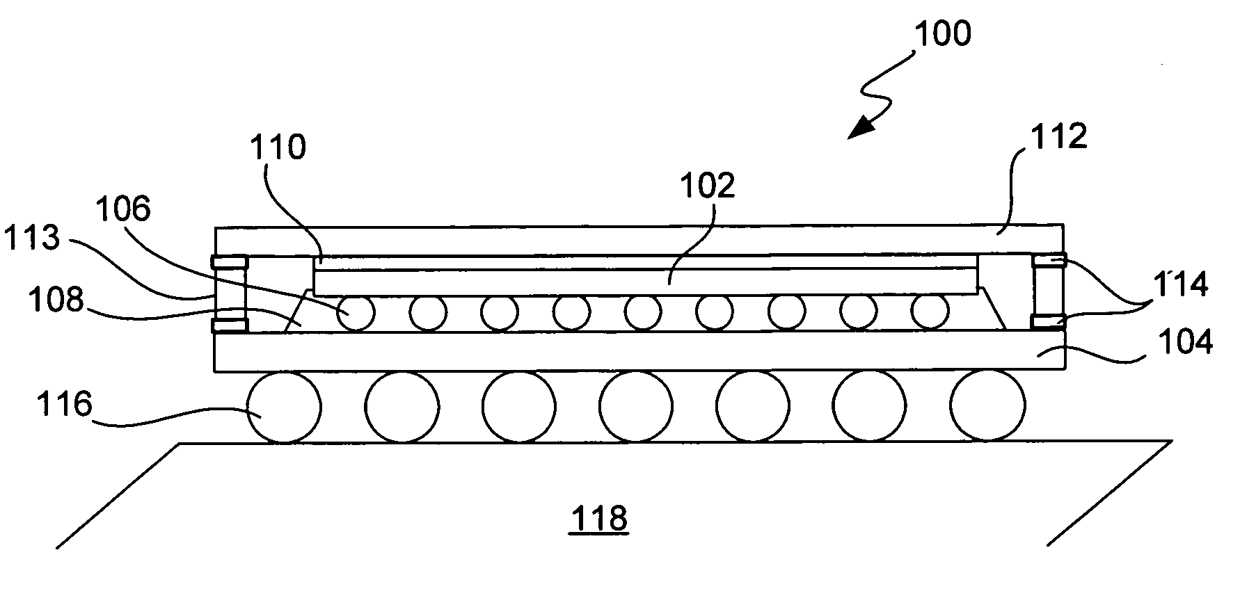
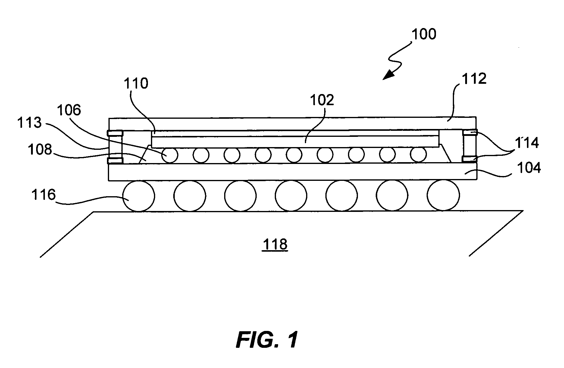
Structure and material for assembling a low-K Si die to achieve a low warpage and industrial grade reliability flip chip package with organic substrate
PatentInactiveUS7144756B1
Innovation
- The implementation of a low-K Si die flip chip package with a heat spreader connected using a high modulus thermal interface material and a low modulus adhesive, redistributing stress and minimizing bowing, thereby enhancing co-planarity and reliability by accommodating thermal cycling without impairing the low-K Si die's performance.
Package with low-warpage carrier
PatentPendingUS20240222234A1
Innovation
- A package manufacturing method involving a pre-warped carrier with electronic components mounted using a solder structure, where ambient conditions during soldering and cooling cause the carrier to re-warp, reducing warpage in the mounting plane to less than 50 μm by managing the coefficient of thermal expansion mismatch between the carrier and electronic components.


Thermal Management Integration Strategies
The integration of thermal management systems with low-warpage packaging solutions represents a critical convergence of two essential design requirements in modern electronics. Effective thermal management strategies must be carefully balanced against warpage control mechanisms to ensure optimal package performance without compromising structural integrity.
Advanced thermal interface materials (TIMs) play a pivotal role in this integration approach. Modern TIMs are engineered with controlled thermal expansion coefficients that complement the warpage mitigation strategies of the overall package design. These materials utilize phase-change compounds and thermally conductive polymers that maintain consistent thermal pathways while minimizing differential expansion stresses across package interfaces.
Embedded cooling architectures offer sophisticated integration opportunities by incorporating microfluidic channels directly within package substrates. This approach eliminates the need for external thermal management components that could introduce additional warpage-inducing stress points. The embedded channels are strategically positioned to align with the neutral stress zones identified through warpage modeling, ensuring thermal efficiency without structural compromise.
Multi-layer thermal spreading solutions leverage copper-filled via arrays and thermal planes that are co-designed with the package's mechanical stress distribution patterns. These spreading layers are optimized through finite element analysis to provide maximum heat dissipation while reinforcing the package structure against warpage-inducing forces. The thermal via placement follows stress-neutral pathways to avoid creating localized stress concentrations.
Adaptive thermal management systems represent an emerging integration strategy that dynamically adjusts cooling performance based on real-time warpage monitoring. These systems incorporate embedded sensors that detect minute package deformations and automatically modulate thermal management intensity to prevent excessive thermal cycling that could exacerbate warpage issues.
The integration methodology requires comprehensive co-simulation approaches that simultaneously model thermal performance and mechanical stress distribution. This holistic design philosophy ensures that thermal management enhancements do not inadvertently introduce new warpage mechanisms while maintaining the required thermal performance specifications for next-generation electronic packages.
Reliability Testing Standards for Warpage Control
Reliability testing standards for warpage control in electronics packaging components have evolved significantly to address the increasing demands of miniaturization and performance requirements. These standards establish systematic methodologies for measuring, evaluating, and validating warpage behavior under various environmental and operational conditions. The primary objective is to ensure that packaging components maintain dimensional stability throughout their operational lifecycle while meeting stringent reliability requirements.
International standards organizations, including JEDEC, IPC, and ASTM, have developed comprehensive testing protocols specifically targeting warpage measurement and control. JEDEC Standard JESD22-B112 provides detailed procedures for measuring package warpage and twist using shadow moiré and laser interferometry techniques. This standard defines critical measurement parameters, including temperature profiles, measurement intervals, and acceptable warpage thresholds for different package types.
Temperature cycling tests represent a fundamental component of warpage reliability assessment. These tests typically involve exposing packages to temperature ranges from -55°C to +150°C, with specific ramp rates and dwell times designed to simulate real-world thermal stress conditions. The testing protocols evaluate both reversible and irreversible warpage components, distinguishing between elastic deformation and permanent structural changes that may compromise package integrity.
Moisture sensitivity level testing, as defined by IPC/JEDEC J-STD-020, incorporates warpage measurements during reflow simulation processes. This standard establishes correlation between moisture absorption, thermal expansion, and resulting warpage behavior. The testing methodology includes pre-conditioning phases, baking procedures, and real-time warpage monitoring during simulated assembly processes.
Advanced testing methodologies now incorporate real-time warpage monitoring using high-resolution optical measurement systems. These systems enable continuous tracking of warpage evolution during thermal cycling, providing detailed insights into warpage kinetics and failure mechanisms. The integration of statistical analysis methods ensures robust data interpretation and establishes confidence intervals for warpage predictions.
Standardized acceptance criteria define maximum allowable warpage values based on package dimensions, substrate thickness, and intended applications. These criteria consider both absolute warpage values and warpage gradients, ensuring compatibility with assembly processes and long-term reliability requirements. The standards also address measurement uncertainty and repeatability requirements to ensure consistent evaluation across different testing facilities and equipment configurations.
Unlock deeper insights with Patsnap Eureka Quick Research — get a full tech report to explore trends and direct your research. Try now!
Generate Your Research Report Instantly with AI Agent
Supercharge your innovation with Patsnap Eureka AI Agent Platform!