

Magnetic Tunnel Junctions vs Spin Valves: Switching Performance Analysis
MAY 14, 20268 MIN READ
Generate Your Research Report Instantly with AI Agent
PatSnap Eureka helps you evaluate technical feasibility & market potential.
MTJ vs Spin Valve Technology Background and Objectives
Magnetic tunnel junctions and spin valves represent two fundamental spintronic device architectures that have revolutionized the landscape of magnetic memory and sensing technologies. Both technologies emerged from the discovery of giant magnetoresistance effects in the late 1980s and early 1990s, marking the beginning of practical spintronics applications. These devices exploit the spin-dependent transport properties of electrons to achieve controllable resistance states, forming the foundation for modern magnetic random access memory, hard disk drive read heads, and magnetic field sensors.
The evolution of these technologies has been driven by the relentless pursuit of faster switching speeds, lower power consumption, and higher storage densities in magnetic memory applications. Spin valves, consisting of ferromagnetic layers separated by non-magnetic metallic spacers, initially dominated commercial applications due to their relatively simple fabrication processes and robust performance characteristics. However, the emergence of magnetic tunnel junctions, featuring insulating barrier layers that enable quantum tunneling effects, has introduced superior magnetoresistance ratios and enhanced scalability potential.
The switching performance analysis between these two technologies has become increasingly critical as the semiconductor industry approaches fundamental scaling limits. Current technological demands require switching times in the sub-nanosecond regime while maintaining energy efficiency and thermal stability. The comparative evaluation of switching mechanisms reveals distinct advantages and limitations for each approach, with MTJs demonstrating superior resistance ratios but potentially facing challenges in switching speed optimization.
The primary objective of this technological investigation centers on establishing comprehensive performance benchmarks for switching characteristics in both device architectures. This includes analyzing current-induced switching dynamics, voltage-controlled switching mechanisms, and thermally-assisted switching processes. Understanding the fundamental physics governing switching behavior enables the identification of optimization pathways for next-generation spintronic devices.
Furthermore, the research aims to evaluate the scalability prospects of each technology in advanced manufacturing nodes, considering factors such as process complexity, material compatibility, and integration challenges with complementary metal-oxide-semiconductor technologies. The ultimate goal involves providing strategic guidance for technology selection in specific application domains, ranging from embedded memory solutions to standalone storage applications, while considering the trade-offs between performance, power consumption, and manufacturing feasibility.
Market Demand for Advanced Spintronic Memory Solutions
The global memory market is experiencing unprecedented demand for next-generation storage solutions that can overcome the limitations of traditional memory technologies. Current memory architectures face significant challenges including high power consumption, limited endurance, and the growing performance gap between volatile and non-volatile memory systems. This has created substantial market opportunities for spintronic memory technologies, particularly those utilizing magnetic tunnel junctions and spin valve structures.
Enterprise data centers represent the largest addressable market segment for advanced spintronic memory solutions. These facilities require memory systems that can deliver high-speed access while maintaining data persistence and energy efficiency. The exponential growth in data processing requirements, driven by artificial intelligence, machine learning, and big data analytics, has intensified the need for memory technologies that can bridge the gap between fast volatile memory and slower storage systems.
Mobile computing and edge devices constitute another critical market segment driving spintronic memory adoption. The proliferation of smartphones, tablets, and Internet of Things devices has created demand for memory solutions that combine high performance with ultra-low power consumption. Spintronic technologies offer the potential to extend battery life while providing instant-on capabilities and improved system responsiveness.
Automotive electronics represents an emerging high-growth market for spintronic memory applications. Modern vehicles require memory systems capable of operating reliably in harsh environmental conditions while supporting advanced driver assistance systems, autonomous driving features, and in-vehicle entertainment systems. The automotive industry's transition toward electric and autonomous vehicles has further amplified the demand for robust, high-performance memory solutions.
The industrial automation and aerospace sectors are increasingly adopting spintronic memory technologies for mission-critical applications. These markets require memory systems that can withstand extreme temperatures, radiation, and mechanical stress while maintaining data integrity over extended periods. The unique properties of magnetic tunnel junctions and spin valves make them particularly suitable for these demanding applications.
Market dynamics are also influenced by the semiconductor industry's ongoing efforts to continue scaling beyond traditional CMOS limitations. As conventional memory technologies approach physical scaling limits, spintronic solutions offer a pathway to maintain performance improvements while reducing power consumption and increasing integration density.
Current MTJ and Spin Valve Switching Limitations
Magnetic Tunnel Junctions (MTJs) and spin valves face several fundamental switching limitations that constrain their performance in practical applications. The primary challenge for MTJs lies in the thermal stability paradox, where achieving fast switching speeds conflicts with maintaining adequate data retention. Current MTJ devices require switching currents in the range of 10^5 to 10^6 A/cm², which generates significant Joule heating and reduces device reliability. The critical switching current density remains inversely proportional to the thermal stability factor, creating a fundamental trade-off between speed and retention.
Spin valves encounter distinct limitations related to their trilayer structure and current-perpendicular-to-plane (CPP) geometry. The switching mechanism relies on spin-transfer torque, but current spin valves suffer from asymmetric switching behavior between parallel and antiparallel states. This asymmetry results in different switching thresholds and speeds for the two magnetic configurations, complicating circuit design and reducing operational margins.
Both technologies struggle with write error rates that increase exponentially as switching currents approach the thermal noise floor. MTJs typically exhibit write error rates of 10^-6 to 10^-9 at nominal operating conditions, while spin valves show similar error characteristics but with different voltage dependencies. The stochastic nature of thermally-assisted switching introduces probabilistic behavior that becomes more pronounced as device dimensions shrink below 40nm.
Process variation represents another critical limitation affecting both MTJ and spin valve performance. Manufacturing tolerances in barrier thickness, electrode composition, and interface quality directly impact switching characteristics. Current fabrication processes yield switching current variations of 15-25% across wafer-scale production, significantly affecting yield and requiring substantial design margins.
Endurance limitations further constrain practical deployment, with current MTJ devices demonstrating cycling endurance of 10^12 to 10^15 write cycles before significant degradation occurs. Spin valves typically show lower endurance due to electromigration effects in the metallic spacer layers. Both technologies experience gradual degradation of the tunnel magnetoresistance ratio over extended cycling, ultimately limiting their operational lifetime in high-frequency switching applications.
Current Switching Performance Solutions
01 Magnetic tunnel junction structure optimization for enhanced switching
Optimization of magnetic tunnel junction structures involves engineering the barrier layer thickness, electrode materials, and interface properties to improve switching characteristics. The barrier layer composition and crystalline structure significantly affect the tunneling magnetoresistance ratio and switching voltage. Advanced materials and fabrication techniques are employed to create more efficient magnetic tunnel junctions with reduced switching energy and improved reliability.- Magnetic tunnel junction structure optimization for enhanced switching: Optimization of magnetic tunnel junction structures involves engineering the barrier layer thickness, electrode materials, and interface properties to improve switching characteristics. The barrier layer composition and crystalline structure significantly affect the tunneling magnetoresistance ratio and switching voltage. Advanced materials and fabrication techniques are employed to create more efficient tunnel barriers that enable faster switching speeds and lower power consumption.
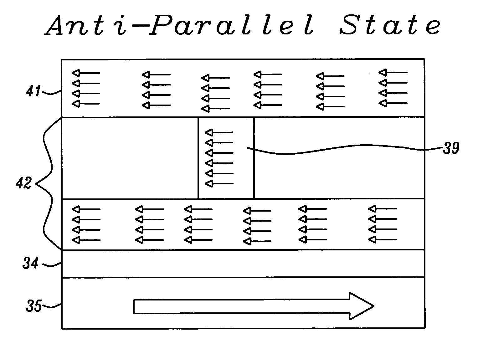
- Spin valve layer stack engineering for improved performance: Spin valve devices utilize carefully designed multilayer stacks with free and pinned magnetic layers separated by non-magnetic spacers. The optimization involves selecting appropriate ferromagnetic materials, controlling layer thicknesses, and managing interlayer coupling effects. Advanced antiferromagnetic pinning layers and synthetic antiferromagnet structures are implemented to enhance thermal stability and reduce switching fields while maintaining high magnetoresistance ratios.
- Current-induced switching mechanisms and spin-transfer torque: Current-induced switching utilizes spin-polarized currents to manipulate magnetization states through spin-transfer torque effects. This approach enables electrical control of magnetic states without external magnetic fields. The switching efficiency depends on current density, pulse duration, and the spin polarization of the current. Optimization involves engineering the current paths and magnetic anisotropy to achieve reliable switching at reduced current densities.
- Thermal stability and retention characteristics enhancement: Thermal stability is crucial for maintaining magnetic states and ensuring reliable device operation across temperature ranges. Enhancement strategies include optimizing magnetic anisotropy energy, controlling grain size and crystalline orientation, and implementing temperature-compensated designs. The retention characteristics are improved through careful selection of magnetic materials with appropriate coercivity and thermal stability coefficients to prevent unwanted switching due to thermal fluctuations.
- Write and read operation optimization for memory applications: Memory applications require optimized write and read operations to achieve fast access times and reliable data storage. Write optimization involves controlling switching pulses, current amplitudes, and timing sequences to ensure consistent state transitions. Read operations are enhanced through signal amplification techniques and noise reduction methods. The integration of sensing circuits and reference systems improves the distinction between different resistance states and enhances overall memory performance.
02 Spin valve configuration and layer stack engineering
Spin valve devices utilize carefully engineered multilayer stacks with free and pinned magnetic layers separated by non-magnetic spacers. The optimization involves selecting appropriate materials for each layer, controlling thickness, and managing magnetic coupling between layers. Advanced antiferromagnetic pinning layers and synthetic antiferromagnet structures are implemented to enhance thermal stability and reduce switching fields while maintaining high magnetoresistance ratios.Expand Specific Solutions03 Current-induced switching mechanisms and spin-transfer torque
Current-induced switching utilizes spin-polarized currents to manipulate magnetization states through spin-transfer torque effects. This mechanism enables electrical control of magnetic states without external magnetic fields. The switching efficiency depends on current density, pulse duration, and the magnetic anisotropy of the free layer. Optimization strategies focus on reducing critical switching currents while maintaining switching reliability and speed.Expand Specific Solutions04 Thermal stability and retention characteristics
Thermal stability is crucial for maintaining data integrity in magnetic memory devices. The energy barrier between magnetic states must be sufficiently high to prevent thermally activated switching while allowing controlled electrical switching. Material selection, magnetic anisotropy engineering, and device geometry optimization are key factors in achieving the required thermal stability. Advanced measurement techniques are used to characterize retention properties under various temperature conditions.Expand Specific Solutions05 Device fabrication and process optimization
Manufacturing processes for magnetic tunnel junctions and spin valves require precise control of deposition conditions, annealing treatments, and patterning techniques. Critical aspects include maintaining clean interfaces, controlling oxidation levels in barrier layers, and minimizing process-induced damage. Advanced lithography and etching processes are employed to achieve the required device dimensions while preserving magnetic and electrical properties. Quality control measures ensure consistent device performance across wafer-scale production.Expand Specific Solutions
Key Players in MTJ and Spin Valve Industry
The magnetic tunnel junctions versus spin valves switching performance analysis represents a mature technology domain within the spintronics industry, currently in its commercialization phase with established market applications in memory devices and sensors. The market demonstrates significant scale, driven by demand for non-volatile memory solutions and advanced storage technologies. Technology maturity varies across key players, with established semiconductor giants like Intel, IBM, Micron Technology, and Taiwan Semiconductor Manufacturing leading in manufacturing capabilities and integration expertise. Memory specialists including KIOXIA, Headway Technologies, Grandis, and Avalanche Technology focus on specialized spintronic applications. Research institutions such as Cornell University, Chinese Academy of Sciences Institute of Physics, and CEA contribute fundamental advances, while companies like Infineon, Hitachi, and NEC drive industrial implementation. The competitive landscape shows convergence toward practical applications with ongoing performance optimization efforts.
Micron Technology, Inc.
Technical Solution: Micron has developed high-performance STT-MRAM using optimized MTJ structures with dual MgO barriers achieving tunnel magnetoresistance ratios exceeding 300% and retention times over 10 years at 85°C. Their switching optimization focuses on reducing write error rates to below 10^-9 through precise control of switching pulse width and amplitude. The company employs advanced materials engineering including boron-doped CoFeB electrodes and crystalline MgO barriers to enhance switching reliability and reduce device-to-device variations. Micron's MTJ technology demonstrates switching currents around 100μA with sub-nanosecond switching capabilities for high-speed memory applications.
Strengths: Excellent reliability and retention characteristics with low write error rates suitable for commercial memory products. Weaknesses: Higher switching currents compared to leading competitors and challenges in further scaling while maintaining performance consistency.
International Business Machines Corp.
Technical Solution: IBM has developed advanced MTJ-based MRAM technology with perpendicular magnetic anisotropy (PMA) structures that achieve switching currents as low as 50μA and switching times under 10ns. Their STT-MRAM solutions demonstrate superior thermal stability up to 400°C and endurance exceeding 10^12 cycles. IBM's approach utilizes CoFeB/MgO/CoFeB MTJ stacks with optimized interfacial engineering to reduce critical switching current while maintaining high tunnel magnetoresistance ratios above 200%. The company has successfully integrated these MTJs into 22nm FinFET processes for embedded memory applications.
Strengths: Industry-leading switching performance with ultra-low power consumption and high thermal stability. Weaknesses: Complex manufacturing processes requiring precise control of interfacial properties and higher production costs compared to conventional memory technologies.
Core Patents in MTJ vs Spin Valve Switching
Spin torque transfer MRAM design with low switching current
PatentInactiveUS20100315869A1
Innovation
- The introduction of a spin filtering layer (SFL) and a nano-current channel (NCC) structure, where the SFL has a preferred magnetization direction opposite to the pinned layer and is not switched by the spin current, and the NCC confines current locally to maximize density, optimizing coupling strength between layers to reduce the critical switching current.

Magnetic Materials Having Superparamagnetic Particles
PatentInactiveUS20110039020A1
Innovation
- Incorporating superparamagnetic particles on the surface or within magnetic films, which can be patterned and embedded in non-magnetic host materials, to increase damping and decrease coercivity, thereby improving the switching characteristics and energy efficiency of magnetic devices.


Manufacturing Process Optimization Strategies
Manufacturing process optimization for magnetic tunnel junctions (MTJs) and spin valves requires fundamentally different approaches due to their distinct structural complexities and performance requirements. MTJ fabrication demands precise control over barrier layer thickness, typically requiring atomic-level deposition accuracy of 0.8-1.2 nanometers for the MgO tunnel barrier. Advanced sputtering techniques with real-time thickness monitoring and temperature-controlled substrates have emerged as critical optimization strategies to achieve consistent tunneling magnetoresistance ratios exceeding 200%.
Spin valve manufacturing processes focus primarily on optimizing the antiferromagnetic pinning layer and free layer interfaces. Key optimization strategies include implementing seed layer engineering to control crystallographic texture and grain size distribution. Ultra-high vacuum conditions below 10^-9 Torr during deposition significantly improve interface quality and reduce oxidation-related defects that compromise switching performance.
Thermal management during fabrication represents a crucial optimization parameter for both device types. MTJs require carefully controlled annealing processes at temperatures between 300-400°C to crystallize the MgO barrier while maintaining magnetic properties. Spin valves benefit from lower temperature processing to preserve antiferromagnetic exchange coupling, typically requiring optimization of deposition temperatures below 250°C.
Advanced lithography techniques have become essential for achieving sub-100nm device dimensions with minimal edge damage. Electron beam lithography combined with ion beam etching optimization reduces sidewall roughness and prevents magnetic domain formation at device edges. Process parameter optimization includes ion beam angle control, etch rate modulation, and post-etch surface treatment protocols.
Quality control integration throughout the manufacturing workflow enables real-time process adjustments. In-situ magnetic property monitoring during deposition allows immediate correction of layer thickness variations or composition deviations. Statistical process control implementation with automated feedback loops has demonstrated significant improvements in device-to-device uniformity and yield optimization across wafer-scale production environments.
Energy Efficiency and Thermal Management Considerations
Energy efficiency represents a critical performance differentiator between magnetic tunnel junctions (MTJs) and spin valves in spintronic applications. MTJs demonstrate superior energy efficiency due to their higher tunnel magnetoresistance ratios, typically ranging from 100% to 600%, compared to spin valves which achieve 10-20% magnetoresistance. This enhanced efficiency translates directly to reduced power consumption during read operations, as lower current densities are required to detect resistance states.
The switching energy requirements reveal distinct characteristics between these technologies. MTJs require spin-transfer torque currents in the range of 10^5 to 10^6 A/cm² for reliable switching, while spin valves typically demand higher current densities due to their lower spin polarization efficiency. However, MTJs benefit from voltage-controlled magnetic anisotropy effects, enabling potential energy reductions of up to 100x compared to current-driven switching mechanisms.
Thermal management challenges differ significantly between MTJ and spin valve architectures. MTJs exhibit better thermal stability due to their crystalline barrier structure, maintaining performance integrity at elevated temperatures up to 350°C. The tunnel barrier effectively isolates the magnetic layers, reducing thermal-induced magnetic coupling variations that commonly affect spin valve performance above 200°C.
Heat dissipation patterns show MTJs generating localized heating primarily at the barrier interface during switching events, while spin valves distribute thermal energy across multiple metallic layers. This concentrated heating in MTJs can be advantageous for targeted thermal management strategies but requires careful consideration of barrier integrity under repeated thermal cycling.
Power scaling considerations favor MTJs for high-density applications, as their exponential resistance dependence on barrier thickness enables aggressive device miniaturization while maintaining energy efficiency. Spin valves face fundamental limitations in power scaling due to their linear resistance characteristics and increased susceptibility to thermal fluctuations at reduced dimensions, making them less suitable for next-generation low-power spintronic systems.
Unlock deeper insights with PatSnap Eureka Quick Research — get a full tech report to explore trends and direct your research. Try now!
Generate Your Research Report Instantly with AI Agent
Supercharge your innovation with PatSnap Eureka AI Agent Platform!