

Optimize Backside Metallization for Solar Cell Applications
APR 15, 20269 MIN READ
Generate Your Research Report Instantly with AI Agent
PatSnap Eureka helps you evaluate technical feasibility & market potential.
Solar Cell BSF Technology Background and Objectives
Solar cell technology has undergone remarkable evolution since the first practical photovoltaic cell was developed at Bell Laboratories in 1954. The continuous pursuit of higher efficiency and lower manufacturing costs has driven innovations across all components of solar cells, with backside metallization emerging as a critical factor in determining overall device performance. The backside contact system serves multiple essential functions including current collection, electrical conductivity enhancement, and optical reflection optimization.
The Back Surface Field (BSF) technology represents a pivotal advancement in solar cell design, fundamentally addressing efficiency limitations caused by rear surface recombination losses. Traditional solar cells without BSF structures suffer from significant carrier recombination at the rear contact interface, which substantially reduces the overall conversion efficiency. The BSF creates an electric field that repels minority carriers from the rear surface, effectively reducing recombination velocity and improving carrier collection efficiency.
Historical development of BSF technology began with aluminum-based solutions in the 1970s, where aluminum paste was screen-printed and fired to create a p+ region through aluminum-silicon alloying. This approach provided both electrical contact and BSF functionality simultaneously. However, the aluminum BSF approach, while cost-effective, presents limitations in terms of surface recombination velocity and contact resistance, particularly for high-efficiency cell architectures.
The primary objective of optimizing backside metallization for solar cell applications centers on maximizing power conversion efficiency while maintaining manufacturing feasibility and cost-effectiveness. This involves achieving optimal balance between electrical performance, optical properties, and mechanical reliability. Key performance targets include minimizing contact resistance, reducing surface recombination velocity below 100 cm/s, and maximizing internal light reflection to enhance photon utilization.
Advanced BSF technologies now encompass various approaches including passivated emitter and rear cell (PERC) structures, aluminum oxide passivation layers, and selective contact schemes. These developments aim to achieve superior passivation quality while maintaining excellent electrical contact properties. The integration of dielectric passivation layers with localized metal contacts represents the current frontier in BSF optimization, enabling efficiency improvements of 0.5-1.0% absolute compared to conventional aluminum BSF cells.
Future objectives focus on developing next-generation backside metallization schemes that can support cell efficiencies exceeding 24% for industrial production. This includes exploring novel materials, advanced patterning techniques, and innovative contact formation processes that can deliver superior performance while remaining compatible with high-throughput manufacturing requirements.
Market Demand for High-Efficiency Solar Cell BSF Solutions
The global solar photovoltaic market continues to experience unprecedented growth driven by increasing environmental consciousness, declining installation costs, and supportive government policies worldwide. This expansion has intensified the demand for high-efficiency solar cell technologies, particularly those incorporating advanced backside field (BSF) solutions that can maximize energy conversion rates while maintaining cost-effectiveness.
Traditional aluminum BSF technology, while widely adopted due to its simplicity and low cost, faces significant limitations in achieving the efficiency levels demanded by modern applications. The industry increasingly requires BSF solutions capable of delivering cell efficiencies exceeding twenty-two percent, driving substantial interest in alternative approaches such as passivated emitter and rear cell (PERC) technology, aluminum oxide passivation, and selective emitter designs.
Commercial and utility-scale solar installations represent the primary demand drivers for high-efficiency BSF solutions. These large-scale deployments prioritize long-term energy yield and return on investment, making the premium costs associated with advanced BSF technologies economically justifiable. The residential market segment also demonstrates growing appetite for high-efficiency solutions, particularly in regions with limited roof space where maximizing power density becomes critical.
Emerging applications in electric vehicle integration, building-integrated photovoltaics, and portable electronics create additional market segments demanding specialized BSF characteristics. These applications often require enhanced performance under varying temperature conditions, improved mechanical durability, and optimized form factors that challenge conventional BSF design approaches.
Regional market dynamics significantly influence BSF solution requirements. Asian markets, led by China and India, emphasize cost-effective efficiency improvements suitable for large-scale manufacturing. European markets prioritize premium efficiency solutions aligned with stringent environmental regulations and space constraints. North American markets demonstrate balanced demand across efficiency tiers, with increasing focus on domestic manufacturing capabilities.
The competitive landscape reveals intensifying pressure on solar cell manufacturers to differentiate their products through superior BSF performance. This market dynamic accelerates adoption of advanced metallization techniques, novel material compositions, and innovative processing methods that can deliver measurable efficiency gains while maintaining manufacturing scalability and economic viability for widespread deployment.
Current BSF Metallization Challenges and Technical Barriers
The metallization of back surface field (BSF) structures in solar cells faces significant technical barriers that limit overall device performance and manufacturing scalability. Traditional aluminum-based BSF metallization encounters fundamental challenges related to contact resistance, thermal stability, and process compatibility with advanced cell architectures.
Contact resistance remains a primary concern in BSF metallization, particularly at the metal-semiconductor interface. Conventional screen-printed aluminum pastes often exhibit non-uniform contact formation due to inconsistent alloying processes during firing. The aluminum-silicon eutectic formation at 577°C creates localized heavily doped regions, but this process is difficult to control precisely, leading to variable contact quality across the cell surface. Poor contact uniformity results in increased series resistance and reduced fill factor performance.
Thermal processing limitations present another critical barrier in BSF optimization. The high-temperature firing required for aluminum paste sintering can cause unwanted diffusion effects and crystal defect formation. These thermal cycles often exceed 800°C, which can degrade the bulk silicon quality and create recombination centers that reduce minority carrier lifetime. Additionally, thermal stress from coefficient of thermal expansion mismatches between aluminum and silicon can induce microcracks and mechanical reliability issues.
Process integration challenges become increasingly complex with advanced cell structures such as PERC and bifacial designs. Traditional BSF metallization processes are incompatible with rear-side passivation layers, requiring selective contact formation through dielectric films. The laser ablation and local contact opening processes introduce additional complexity and potential yield loss mechanisms. Achieving proper alignment between contact openings and metallization patterns requires precise process control that increases manufacturing costs.
Material compatibility issues further complicate BSF metallization optimization. Alternative metals such as silver or copper offer superior electrical conductivity but face challenges with silicon contact formation and long-term stability. Silver migration and copper contamination risks necessitate barrier layer implementations that add process complexity. The development of low-temperature sintering pastes to address thermal budget constraints often compromises adhesion strength and electrical performance.
Manufacturing scalability represents a significant barrier for advanced BSF metallization approaches. While laboratory demonstrations show promising results with novel contact materials and formation techniques, translating these innovations to high-throughput production environments remains challenging. Process window optimization, equipment modifications, and quality control implementations require substantial capital investment and extended development timelines that limit commercial adoption rates.
Current BSF Optimization Solutions and Approaches
01 Backside metallization methods for solar cells
Various methods and techniques are employed for applying metallization to the backside of solar cells to improve electrical conductivity and overall cell performance. These methods include screen printing, physical vapor deposition, and electroplating processes. The backside metallization layer typically serves as an electrical contact and can incorporate different metal compositions to optimize conductivity and adhesion properties.- Backside metallization for solar cells: Backside metallization techniques are employed in solar cell manufacturing to create electrical contacts on the rear surface of photovoltaic devices. These methods involve depositing conductive materials such as aluminum, silver, or copper onto the backside to improve electrical conductivity and enhance cell efficiency. Various deposition techniques including screen printing, physical vapor deposition, and electroplating are utilized to form uniform metal layers that facilitate electron collection and reduce contact resistance.
- Backside metallization for semiconductor devices: In semiconductor device fabrication, backside metallization involves applying metal layers to the rear surface of wafers or chips to provide electrical grounding, heat dissipation, and mechanical support. This process is critical for power devices, integrated circuits, and microelectronic components. The metallization layer typically serves as a die attach surface and helps in thermal management by conducting heat away from active regions.
- Advanced backside metallization structures and patterns: Advanced metallization structures incorporate patterned or selective metal deposition on the backside to optimize device performance. These include localized contact points, grid patterns, or segmented metal regions that reduce shading losses, minimize material usage, and improve current collection efficiency. Such designs are particularly beneficial in high-efficiency solar cells and advanced semiconductor devices where precise control over electrical and optical properties is required.
- Backside metallization using novel materials and composites: Novel materials and composite structures are being developed for backside metallization to enhance adhesion, conductivity, and durability. These include multi-layer metal stacks, alloy compositions, and the integration of barrier layers to prevent diffusion and corrosion. The use of alternative materials aims to reduce manufacturing costs while maintaining or improving electrical and mechanical properties of the metallized backside.
- Process optimization and equipment for backside metallization: Process optimization focuses on improving the efficiency, uniformity, and throughput of backside metallization operations. This includes advancements in deposition equipment, automation of handling systems, and development of new processing techniques such as laser-assisted metallization or inkjet printing. Quality control measures and in-line monitoring systems are also implemented to ensure consistent metal layer properties and reduce defects in high-volume manufacturing environments.
02 Patterned backside metallization structures
Patterned metallization on the backside of semiconductor devices allows for selective contact formation and improved current collection. These patterns can include grid structures, point contacts, or localized contact regions that reduce recombination losses while maintaining good electrical performance. The patterning techniques enable better control over the contact area and can be combined with passivation layers.Expand Specific Solutions03 Backside metallization materials and compositions
Different metal materials and alloy compositions are utilized for backside metallization to achieve desired electrical and mechanical properties. Common materials include aluminum, silver, copper, and various metal alloys. The selection of metallization materials affects factors such as contact resistance, adhesion strength, thermal stability, and compatibility with other cell components. Multi-layer metallization stacks combining different metals can provide optimized performance characteristics.Expand Specific Solutions04 Backside metallization for bifacial solar cells
Specialized backside metallization approaches are developed for bifacial solar cells that can collect light from both sides. These designs require transparent or semi-transparent backside contacts, or strategically placed metallization patterns that allow light transmission while maintaining electrical functionality. The metallization schemes must balance optical transparency with electrical conductivity requirements.Expand Specific Solutions05 Advanced backside metallization processing techniques
Novel processing techniques for backside metallization include laser-assisted methods, selective emitter formation, and advanced firing processes. These techniques aim to improve contact quality, reduce processing costs, and enable finer feature sizes. Integration with passivation layers and the use of fire-through metallization approaches allow for simplified manufacturing while maintaining high efficiency levels.Expand Specific Solutions
Key Players in Solar BSF and Metallization Industry
The backside metallization optimization for solar cells represents a mature yet rapidly evolving market segment within the broader photovoltaic industry, which has reached commercial maturity with global revenues exceeding $200 billion annually. The competitive landscape is dominated by established Chinese manufacturers including Trina Solar, LONGi Green Energy, JinkoSolar, and Tongwei Solar, who collectively control significant market share through vertical integration and cost optimization. Technology maturity varies across different metallization approaches, with traditional aluminum-based solutions being well-established while advanced silver-aluminum hybrid systems and novel conductive materials remain in development phases. Equipment suppliers like Applied Materials and Gebr. Schmid provide critical manufacturing infrastructure, while research institutions such as Fraunhofer-Gesellschaft and CEA drive innovation in next-generation metallization techniques. The market demonstrates intense price competition alongside continuous efficiency improvements, with emerging players like Maxeon Solar and established diversified companies like BYD contributing to technological advancement through specialized metallization processes targeting higher cell efficiencies and reduced material costs.
Trina Solar Co., Ltd.
Technical Solution: Trina Solar has implemented advanced screen printing technology combined with selective laser processing for backside metallization optimization. Their approach utilizes high-conductivity aluminum paste formulations with improved rheological properties, enabling finer line printing and reduced contact resistance. The company has developed a dual-layer metallization scheme where a thin adhesion layer is followed by a thicker conductive layer, achieving contact resistivity below 2 mΩ·cm². Their process includes optimized firing profiles with precise temperature control to minimize aluminum spiking while ensuring good ohmic contact formation. Recent innovations include the integration of selective emitter technology with localized heavy doping beneath contact areas to further reduce recombination losses.
Strengths: Cost-effective manufacturing processes and strong integration capabilities across the solar cell production line. Weaknesses: Limited flexibility in adapting to next-generation cell architectures and dependence on paste supplier innovations.
Fraunhofer-Gesellschaft eV
Technical Solution: Fraunhofer Institute has pioneered laser-based selective metallization techniques for backside contacts, including Laser Contact Opening (LCO) and Laser Fired Contacts (LFC) technologies. Their research focuses on femtosecond laser processing to create precise contact openings through dielectric passivation layers without thermal damage to underlying silicon. The institute has developed novel metal plating processes using electroless nickel followed by copper deposition, achieving contact resistances below 1 mΩ·cm². Their work includes comprehensive modeling of contact formation mechanisms and optimization of laser parameters for different cell architectures. Recent developments include integration with heterojunction and TOPCon cell technologies, demonstrating efficiency improvements of up to 0.5% absolute through optimized backside metallization schemes.
Strengths: Cutting-edge research capabilities and strong fundamental understanding of contact physics and laser processing. Weaknesses: Technology transfer challenges from laboratory to industrial scale production and higher processing complexity.
Core Patents in Advanced BSF Metallization Techniques
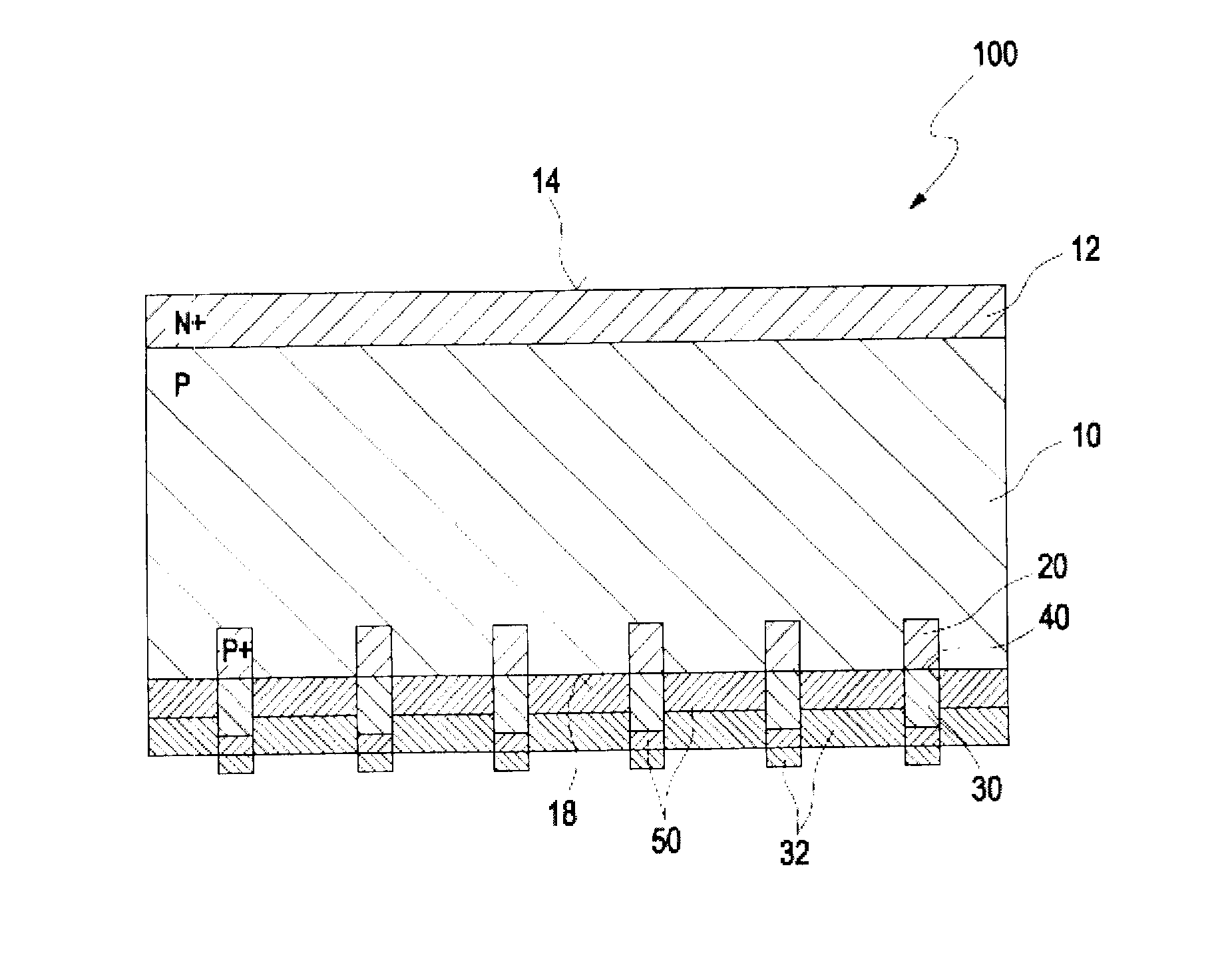
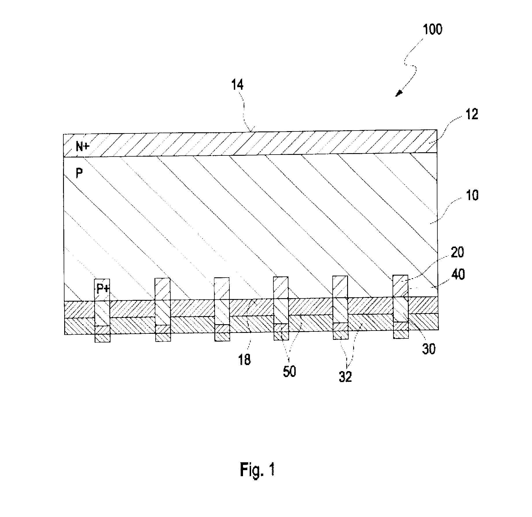
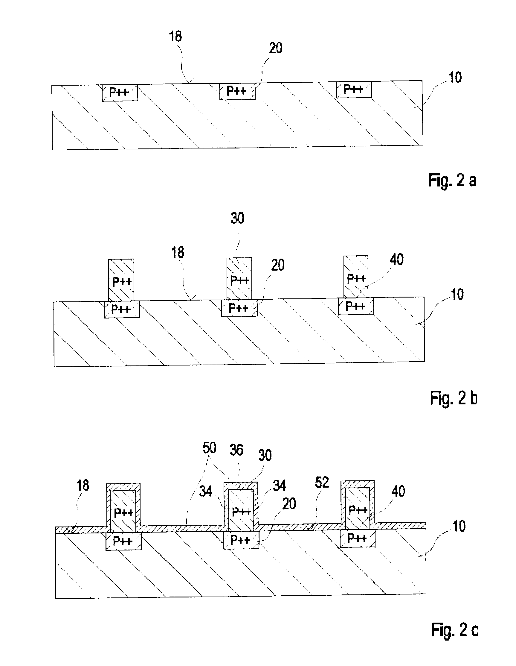
Back passivation solar cell and manufacturing method thereof
PatentActiveCN104091843A
Innovation
- Multiple silver line segment contact areas are used in the back passivation film. The shape of the silver line segments is parallel and staggered in multiple rows. Combined with the back aluminum layer, it reduces silver consumption and reduces the contact area between the back aluminum layer and the silicon substrate. Localized contacts are formed through sintering to improve cell efficiency.


Manufacturing process for making photovoltaic solar cells
PatentInactiveUS20110318865A1
Innovation
- A manufacturing process that involves creating high doped areas on the rear side of the solar cell, providing localized metal contacts on these areas, applying a passivation layer that leaves the contacts free, and depositing a metal layer for the backside field, allowing for improved electrical contact without penetrating the dielectric layer, thus reducing thermal load and integrating well into existing production flows.

Environmental Impact Assessment of BSF Materials
The environmental impact assessment of Back Surface Field (BSF) materials in solar cell applications has become increasingly critical as the photovoltaic industry scales toward terawatt-level deployment. Traditional aluminum-based BSF systems, while cost-effective and widely adopted, present significant environmental challenges throughout their lifecycle. The aluminum paste used in conventional screen-printing processes contains organic solvents and glass frits that generate volatile organic compounds during firing, contributing to air pollution and requiring specialized waste treatment facilities.
Silicon-based BSF alternatives, particularly those utilizing phosphorus or boron diffusion processes, demonstrate substantially lower environmental footprints. These approaches eliminate the need for metal pastes and reduce material consumption by up to 60% compared to aluminum BSF configurations. However, the diffusion processes require high-temperature treatments and specialized gas handling systems for dopant delivery, which increase energy consumption during manufacturing.
Emerging passivated emitter and rear cell (PERC) architectures with dielectric BSF layers offer promising environmental benefits. The aluminum oxide and silicon nitride films used in these structures require minimal material quantities and can be deposited using plasma-enhanced chemical vapor deposition with reduced chemical waste generation. Life cycle assessments indicate that PERC-based BSF systems reduce carbon emissions by approximately 15-20% compared to conventional aluminum BSF during the manufacturing phase.
The end-of-life recyclability of BSF materials presents varying environmental implications. Aluminum-based systems benefit from established recycling infrastructure, with aluminum recovery rates exceeding 90% in mature markets. Conversely, silicon-based and dielectric BSF materials require specialized separation techniques, though they generate fewer toxic byproducts during recycling processes.
Water consumption and chemical waste generation represent additional environmental considerations. Traditional aluminum BSF processing requires extensive cleaning steps using hydrofluoric acid and other hazardous chemicals, generating contaminated wastewater streams. Advanced BSF architectures utilizing atomic layer deposition or ion implantation techniques significantly reduce water usage and chemical waste, though they demand higher initial energy investments for equipment operation.
Cost-Performance Analysis of BSF Manufacturing Processes
The cost-performance analysis of Back Surface Field (BSF) manufacturing processes reveals significant variations across different technological approaches, with aluminum-based BSF remaining the most economically viable option for standard crystalline silicon solar cells. Traditional screen-printed aluminum BSF processes demonstrate manufacturing costs ranging from $0.008 to $0.012 per watt, primarily driven by material consumption, processing time, and equipment utilization rates. The aluminum paste typically accounts for 60-70% of the total BSF processing cost, while firing and handling operations contribute the remaining expenses.
Advanced BSF technologies, including Local Back Surface Field (LBSF) and Passivated Emitter and Rear Cell (PERC) structures, present higher initial manufacturing costs but deliver superior performance metrics. PERC technology, despite requiring additional processing steps and specialized equipment, achieves cost parity at production volumes exceeding 500MW annually due to enhanced cell efficiency gains of 0.8-1.2% absolute. The manufacturing cost premium of $0.015-0.025 per watt is offset by improved power output and reduced balance-of-system costs in photovoltaic installations.
Emerging BSF manufacturing approaches, such as laser-fired contacts and selective emitter technologies, demonstrate promising cost-performance trajectories but require substantial capital investments. These processes exhibit manufacturing costs 15-25% higher than conventional methods during initial deployment phases, yet offer potential cost reductions through improved material utilization and reduced silver consumption. The learning curve analysis indicates that doubling production capacity typically reduces manufacturing costs by 12-18% for advanced BSF processes.
Equipment depreciation represents a critical cost component, particularly for high-throughput manufacturing lines processing over 6000 wafers per hour. The capital expenditure per megawatt of annual capacity ranges from $0.8M to $2.5M depending on the BSF technology complexity and automation level. Process yield rates significantly impact overall cost-performance metrics, with premium BSF technologies requiring yield rates above 98% to maintain economic competitiveness against standard aluminum BSF approaches.
Unlock deeper insights with PatSnap Eureka Quick Research — get a full tech report to explore trends and direct your research. Try now!
Generate Your Research Report Instantly with AI Agent
Supercharge your innovation with PatSnap Eureka AI Agent Platform!