

Optimize Chip Package Assembly Time for Cost Reduction
APR 7, 20269 MIN READ
Generate Your Research Report Instantly with AI Agent
PatSnap Eureka helps you evaluate technical feasibility & market potential.
Chip Package Assembly Optimization Background and Objectives
The semiconductor industry has experienced unprecedented growth over the past decades, driven by increasing demand for electronic devices across consumer, automotive, industrial, and telecommunications sectors. As chip functionality continues to expand while device form factors shrink, the complexity of semiconductor packaging has increased dramatically. This evolution has created significant pressure on manufacturing costs, with assembly processes representing a substantial portion of overall production expenses.
Chip package assembly encompasses multiple critical steps including die attach, wire bonding, encapsulation, and final testing. Each stage requires precise control of materials, equipment, and environmental conditions to ensure product quality and reliability. Traditional assembly methods, while proven effective, often involve lengthy cycle times that directly impact manufacturing throughput and cost efficiency. The industry faces mounting pressure to reduce these cycle times without compromising quality standards.
Current market dynamics further intensify the need for assembly optimization. Rising labor costs in traditional manufacturing regions, coupled with increasing material expenses and energy costs, have compressed profit margins across the supply chain. Simultaneously, customers demand shorter lead times and more competitive pricing, creating a challenging environment where operational efficiency becomes paramount to business sustainability.
The primary objective of optimizing chip package assembly time centers on achieving significant cost reduction while maintaining or improving product quality metrics. This involves identifying bottlenecks in existing assembly processes, implementing advanced automation technologies, and developing innovative methodologies that can accelerate production cycles. Key performance indicators include reducing overall assembly time by 20-30%, minimizing material waste, and improving first-pass yield rates.
Secondary objectives encompass enhancing manufacturing flexibility to accommodate diverse product portfolios and varying production volumes. This includes developing scalable solutions that can adapt to different package types and sizes without requiring extensive retooling or reconfiguration. Additionally, the optimization effort aims to improve predictability in production scheduling and reduce variability in cycle times.
The strategic importance of this optimization extends beyond immediate cost savings. Faster assembly processes enable manufacturers to respond more quickly to market demands, reduce inventory holding costs, and improve cash flow cycles. Furthermore, enhanced efficiency creates competitive advantages that can translate into increased market share and improved customer satisfaction through shorter delivery times and more competitive pricing structures.
Market Demand for Cost-Effective Semiconductor Packaging
The semiconductor packaging industry is experiencing unprecedented demand driven by the proliferation of electronic devices across multiple sectors. Consumer electronics, automotive systems, industrial automation, and emerging technologies such as artificial intelligence and Internet of Things applications are creating substantial pressure for high-volume, cost-effective packaging solutions. This surge in demand has intensified the focus on manufacturing efficiency, particularly in assembly processes where time optimization directly translates to cost reduction and improved market competitiveness.
Market dynamics reveal a clear preference for packaging solutions that balance performance requirements with economic viability. Original equipment manufacturers are increasingly scrutinizing their supply chains, demanding faster turnaround times without compromising quality standards. The automotive sector, in particular, has become a significant driver of packaging innovation, requiring robust solutions that can withstand harsh operating conditions while maintaining cost-effectiveness for mass production applications.
The competitive landscape has shifted toward companies that can demonstrate superior manufacturing efficiency and cost optimization capabilities. Market leaders are differentiating themselves through advanced assembly techniques that reduce cycle times while maintaining high yield rates. This trend has created opportunities for packaging service providers who can offer streamlined processes and innovative approaches to traditional assembly challenges.
Emerging market segments, including edge computing devices, wearable technology, and electric vehicle components, are establishing new benchmarks for packaging requirements. These applications demand compact, reliable solutions that can be produced at scale with minimal manufacturing overhead. The convergence of these market forces has established assembly time optimization as a critical competitive advantage rather than merely an operational improvement.
Supply chain considerations further amplify the importance of efficient packaging processes. Global semiconductor shortages and geopolitical tensions have highlighted the need for resilient, cost-effective manufacturing capabilities. Companies that can reduce assembly times while maintaining quality standards are better positioned to respond to market fluctuations and capitalize on emerging opportunities in the rapidly evolving semiconductor landscape.
Current Assembly Time Bottlenecks and Technical Challenges
The semiconductor packaging industry faces significant assembly time bottlenecks that directly impact production costs and manufacturing efficiency. Current assembly processes are constrained by several critical factors that limit throughput and increase per-unit manufacturing expenses.
Die bonding operations represent one of the most significant time-consuming stages in chip package assembly. The precision required for accurate die placement, combined with the curing time needed for adhesive materials, creates substantial throughput limitations. Traditional epoxy-based die attach processes require thermal curing cycles that can extend from several minutes to hours, depending on package complexity and material specifications.
Wire bonding procedures constitute another major bottleneck, particularly in high pin-count packages. The sequential nature of wire bonding, where each connection must be individually formed, creates inherent speed limitations. Advanced packages requiring hundreds or thousands of interconnections face exponentially increased assembly times. Ball bonding and wedge bonding processes, while reliable, operate at speeds that become economically challenging for complex multi-chip modules.
Molding compound application and curing processes introduce additional time constraints. The injection molding phase requires precise temperature and pressure control, followed by extended curing periods to achieve proper encapsulation integrity. These thermal cycles cannot be significantly accelerated without compromising package reliability or introducing stress-related defects.
Quality inspection and testing procedures embedded within the assembly flow create further time delays. In-line testing requirements, including electrical continuity checks and visual inspections, add cumulative delays that scale with package complexity. Advanced packages requiring comprehensive testing protocols experience proportionally longer assembly cycles.
Material handling and substrate preparation stages contribute to overall assembly time through necessary cleaning, surface treatment, and component positioning operations. Automated handling systems, while improving consistency, operate at fixed speeds that limit overall throughput potential.
Temperature cycling requirements for various assembly stages prevent parallel processing optimization. The need for controlled heating and cooling phases between operations creates mandatory wait times that cannot be eliminated through equipment parallelization alone.
These bottlenecks collectively result in assembly times that can range from several minutes for simple packages to multiple hours for advanced system-in-package solutions, directly translating to increased manufacturing costs and reduced production capacity utilization.
Existing Assembly Time Optimization Solutions
01 Advanced die bonding techniques for reduced assembly time
Implementation of improved die bonding methods and equipment that enable faster attachment of semiconductor chips to substrates or lead frames. These techniques include automated pick-and-place systems, precision alignment mechanisms, and rapid curing adhesives that significantly reduce the time required for die attachment during package assembly. The methods focus on increasing throughput while maintaining bonding quality and reliability.- Advanced die bonding and attachment methods: Innovative die bonding techniques focus on reducing assembly time through improved adhesive application methods, optimized curing processes, and automated placement systems. These methods include rapid thermal bonding, pre-applied adhesive films, and precision pick-and-place equipment that minimize handling time while ensuring reliable chip attachment to substrates or lead frames.
- Wire bonding process optimization: Techniques to accelerate wire bonding include multi-wire bonding capabilities, optimized bonding parameters, and advanced capillary designs that enable faster connection speeds between chip pads and package leads. Automated wire bonding systems with enhanced motion control and pattern recognition reduce cycle time while maintaining bond quality and reliability.
- Molding and encapsulation time reduction: Fast-cure molding compounds and optimized encapsulation processes significantly decrease package assembly time. These innovations include low-viscosity epoxy resins with accelerated curing agents, compression molding techniques with reduced cycle times, and transfer molding systems with improved flow characteristics that enable rapid and uniform encapsulation of semiconductor devices.
- Parallel processing and batch assembly techniques: Manufacturing approaches that enable simultaneous processing of multiple chips or packages reduce overall assembly time. These include gang bonding methods, multi-site molding systems, and parallel testing configurations that allow multiple units to be processed concurrently rather than sequentially, significantly improving throughput and reducing per-unit assembly time.
- Automated inspection and quality control integration: Integrated inline inspection systems and real-time quality monitoring reduce assembly time by eliminating separate inspection steps and enabling immediate feedback for process adjustments. These systems incorporate machine vision, automated optical inspection, and predictive analytics to detect defects during assembly rather than in post-process stages, streamlining the overall manufacturing flow.
02 Wire bonding process optimization
Enhanced wire bonding processes and equipment designed to minimize the time required for electrical interconnection between chip pads and package leads. This includes high-speed wire bonding machines with multiple bonding heads, optimized bonding parameters, and automated loop formation techniques. The improvements enable faster cycle times per bond while ensuring consistent bond quality and reducing overall assembly duration.Expand Specific Solutions03 Parallel processing and multi-chip handling systems
Assembly systems that enable simultaneous processing of multiple chips or packages to reduce overall production time. These systems incorporate parallel processing capabilities, multi-site tooling, and batch handling mechanisms that allow multiple units to be assembled concurrently. The approach significantly increases throughput by performing assembly operations on several devices at once rather than sequentially.Expand Specific Solutions04 Integrated molding and encapsulation processes
Streamlined molding and encapsulation techniques that reduce the time required for package protection and sealing. These methods include rapid-cure molding compounds, optimized mold designs with improved flow characteristics, and integrated heating systems that accelerate curing times. The processes minimize waiting periods between assembly steps and enable faster completion of the encapsulation phase.Expand Specific Solutions05 Automated inspection and testing integration
In-line automated inspection and testing systems integrated into the assembly process to eliminate separate testing steps and reduce overall cycle time. These systems perform real-time quality checks, electrical testing, and defect detection during assembly operations rather than as separate post-assembly steps. The integration enables immediate feedback and reduces the total time from assembly start to finished package verification.Expand Specific Solutions
Key Players in Semiconductor Packaging Industry
The chip package assembly optimization market represents a mature yet rapidly evolving sector driven by increasing demand for cost-effective semiconductor manufacturing. The industry is experiencing significant growth with market expansion fueled by automotive electronics, 5G infrastructure, and IoT applications. Technology maturity varies significantly across market players, with established leaders like Taiwan Semiconductor Manufacturing Co., Samsung Electronics, and Intel Corp. demonstrating advanced automation and AI-driven optimization capabilities. Specialized assembly service providers including ChipMOS Technologies, Powertech Technology, and Advanced Semiconductor Engineering have developed sophisticated turnkey solutions. Equipment manufacturers such as Siemens AG and automation specialists are advancing smart manufacturing technologies. Emerging players like Shanghai Huahong Grace Semiconductor and regional specialists are adopting next-generation assembly techniques. The competitive landscape shows consolidation among tier-one providers while fostering innovation in process optimization, with companies like Synopsys providing critical EDA tools for assembly design optimization.
Taiwan Semiconductor Manufacturing Co., Ltd.
Technical Solution: TSMC implements advanced automated assembly systems with AI-driven process optimization that reduces package assembly time by up to 30% through predictive maintenance and real-time process adjustments. Their CoWoS (Chip-on-Wafer-on-Substrate) technology utilizes high-speed die bonding equipment with throughput rates exceeding 8,000 units per hour. The company employs machine learning algorithms to optimize wire bonding sequences and minimize handling time between assembly stations, achieving cycle time reductions of 15-25% compared to traditional methods.
Strengths: Industry-leading automation technology, extensive R&D investment, proven scalability. Weaknesses: High initial capital investment, complex integration requirements for existing facilities.
Powertech Technology, Inc.
Technical Solution: Powertech focuses on assembly process standardization and equipment optimization to reduce cycle times and manufacturing costs. Their approach includes implementation of high-speed wire bonding systems with multi-head configurations that can process multiple devices simultaneously, achieving throughput increases of 35-40%. The company utilizes statistical process control and machine learning algorithms to optimize assembly parameters in real-time, reducing rework rates by 60% and improving overall assembly efficiency through predictive quality management systems.
Strengths: Specialized in assembly and test services, cost-effective solutions, strong process optimization expertise. Weaknesses: Limited technology differentiation, vulnerable to pricing pressure in competitive markets.
Core Innovations in High-Speed Package Assembly
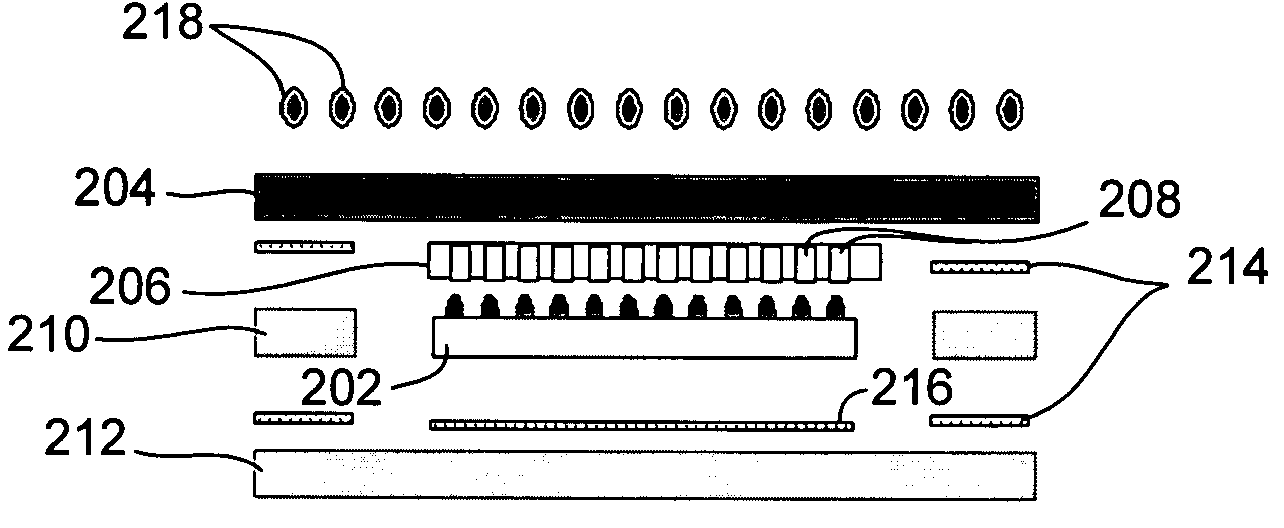
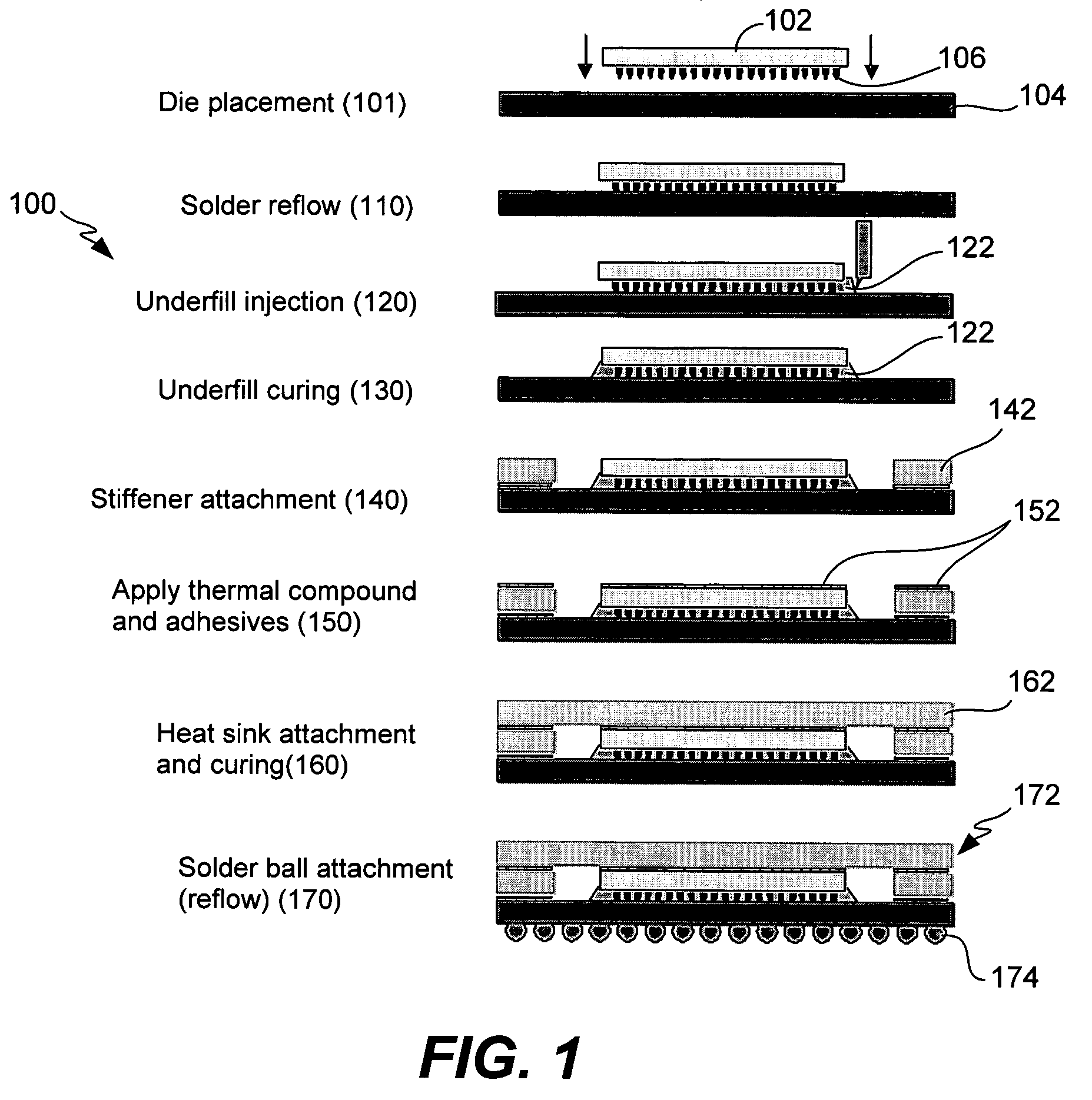
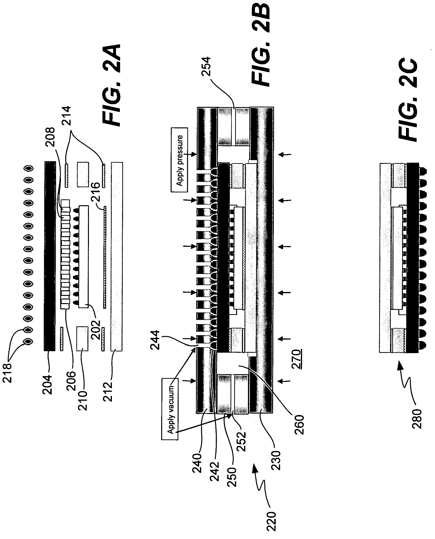
Consolidated flip chip BGA assembly process and apparatus
PatentInactiveUS7262079B2
Innovation
- A consolidated flip chip packaging technique that uses an assembly fixture to align and hold semiconductor package components for a single application of heat and pressure, reducing the process to a few hours and simplifying equipment requirements by employing a self-supporting underfill material and integrating stiffeners and heat spreaders in a single operation.

Chip packaging process including simpification and mergence of burn-in test and high temperature test
PatentInactiveUS20090137069A1
Innovation
- A chip packaging process that integrates substrate-level burn-in testing with post mold curing, where chips are attached to a substrate strip with electrical open sections for isolation, and then encapsulated, allowing for simultaneous curing and burn-in testing before singulation, reducing the need for additional burn-in ovens and minimizing terminal damage.


Supply Chain Impact on Assembly Cost Structure
The semiconductor supply chain's complexity significantly influences chip package assembly cost structures, creating both opportunities and challenges for cost optimization initiatives. Modern assembly operations depend on intricate networks of material suppliers, equipment manufacturers, and service providers, where disruptions or inefficiencies can cascade through the entire cost framework.
Raw material procurement represents the largest cost component in assembly operations, typically accounting for 60-70% of total assembly costs. Critical materials including substrates, bonding wires, encapsulation compounds, and solder materials are sourced from specialized suppliers with varying geographic distributions. Price volatility in these materials directly impacts assembly cost predictability, with substrate costs showing particular sensitivity to supply-demand imbalances.
Equipment and tooling supply chains create substantial capital cost implications for assembly time optimization. Advanced packaging equipment requires significant upfront investments, with lead times often extending 12-18 months for specialized machinery. The concentration of equipment suppliers in specific regions creates supply chain vulnerabilities that can delay optimization projects and increase total cost of ownership through extended procurement cycles.
Labor cost structures vary dramatically across global assembly locations, creating complex trade-offs between direct labor costs and supply chain proximity. While offshore assembly operations offer lower labor rates, extended supply chains increase logistics costs, inventory carrying costs, and quality control expenses. These factors often offset initial labor savings, particularly for high-volume, time-sensitive assembly operations.
Supply chain integration levels significantly impact assembly cost efficiency. Vertically integrated operations demonstrate better cost control through reduced transaction costs and improved coordination, while outsourced models face challenges in cost transparency and optimization alignment. The trend toward supply chain digitalization enables better cost visibility but requires substantial technology investments.
Inventory management strategies within the supply chain directly influence assembly cost structures through working capital requirements and obsolescence risks. Just-in-time approaches minimize carrying costs but increase supply chain coordination complexity, while buffer inventory strategies provide operational flexibility at higher carrying cost penalties.
Quality Control Standards in Accelerated Assembly
Quality control standards in accelerated assembly environments require a fundamental shift from traditional inspection methodologies to real-time monitoring systems. The acceleration of chip package assembly processes introduces unique challenges where conventional quality checkpoints may become bottlenecks, potentially negating the time savings achieved through process optimization. Modern quality control frameworks must therefore integrate seamlessly with high-speed assembly operations while maintaining stringent reliability standards.
Statistical process control becomes critical in accelerated assembly scenarios, where the increased throughput demands more sophisticated sampling strategies. Traditional quality control methods that rely on batch inspection are inadequate for high-speed operations. Instead, continuous monitoring systems utilizing machine learning algorithms can detect anomalies in real-time, enabling immediate corrective actions without halting the entire production line. These systems must establish dynamic control limits that adapt to varying assembly speeds and environmental conditions.
The implementation of in-line inspection technologies represents a cornerstone of quality control in accelerated assembly. Advanced optical inspection systems, X-ray imaging, and automated electrical testing must operate at speeds matching the assembly line throughput. These systems require precise calibration protocols and regular validation procedures to ensure measurement accuracy is not compromised by the increased operational tempo. Integration of multiple inspection modalities provides comprehensive coverage while minimizing false positive rates.
Traceability standards become more complex in accelerated environments where traditional manual documentation methods cannot keep pace with production speeds. Digital quality management systems must capture and correlate quality data across all assembly stages, creating comprehensive quality records for each packaged unit. This requires robust data architecture capable of handling high-volume, high-velocity quality information while maintaining data integrity and accessibility for post-production analysis.
Risk-based quality control strategies optimize inspection resources by focusing on critical quality attributes most likely to impact final product reliability. Accelerated assembly processes must prioritize quality checkpoints based on failure mode analysis and historical defect data. This approach allows for selective intensification of quality control measures at high-risk process steps while streamlining inspection at lower-risk stages, maintaining overall quality assurance without compromising assembly speed objectives.
Unlock deeper insights with PatSnap Eureka Quick Research — get a full tech report to explore trends and direct your research. Try now!
Generate Your Research Report Instantly with AI Agent
Supercharge your innovation with PatSnap Eureka AI Agent Platform!