

Optimize Printed Electronics dielectric thickness for 3.3V reliability
APR 30, 20269 MIN READ
Generate Your Research Report Instantly with AI Agent
PatSnap Eureka helps you evaluate technical feasibility & market potential.
Printed Electronics Dielectric Background and Reliability Goals
Printed electronics represents a transformative manufacturing paradigm that enables the deposition of electronic materials onto flexible substrates through conventional printing processes. This technology has evolved from laboratory curiosities in the 1990s to commercially viable solutions across multiple industries. The fundamental principle involves depositing conductive, semiconductive, and dielectric materials using techniques such as screen printing, inkjet printing, gravure printing, and flexographic printing onto substrates including plastic films, paper, and textiles.
The dielectric layer serves as a critical component in printed electronic devices, functioning as an insulating barrier between conductive elements while maintaining device integrity under operational stress. Traditional silicon-based electronics rely on precisely controlled oxide layers with well-established thickness parameters, but printed electronics face unique challenges due to material properties, processing conditions, and substrate interactions that significantly impact dielectric performance.
Historical development of printed electronics dielectrics began with polymer-based solutions in the early 2000s, progressing through hybrid organic-inorganic materials, and advancing to current nanocomposite formulations. Early implementations suffered from inconsistent thickness control, leading to premature device failure and unreliable performance. The evolution toward more sophisticated material systems has been driven by the need for consistent electrical properties across large-area applications.
The 3.3V operational requirement represents a critical threshold in printed electronics applications, particularly for Internet of Things devices, flexible displays, and wearable electronics. This voltage level demands precise dielectric thickness optimization to prevent breakdown while maintaining manufacturing efficiency. Current industry standards suggest dielectric thickness ranges between 100-500 nanometers for 3.3V applications, but optimal values depend heavily on material composition, processing parameters, and environmental conditions.
Reliability goals for printed electronics dielectrics encompass multiple performance criteria including breakdown voltage stability, leakage current minimization, temperature cycling endurance, and mechanical flexibility retention. The primary objective involves achieving consistent dielectric performance across manufacturing variations while maintaining cost-effectiveness compared to traditional electronics manufacturing. Long-term reliability targets typically specify operational lifetimes exceeding 10,000 hours under continuous 3.3V stress with less than 10% performance degradation.
Contemporary research focuses on establishing predictive models that correlate dielectric thickness with reliability metrics, enabling manufacturers to optimize layer deposition for specific application requirements. The ultimate goal involves developing standardized thickness specifications that ensure reliable 3.3V operation across diverse printed electronics platforms while accommodating the inherent variability of printing processes.
The dielectric layer serves as a critical component in printed electronic devices, functioning as an insulating barrier between conductive elements while maintaining device integrity under operational stress. Traditional silicon-based electronics rely on precisely controlled oxide layers with well-established thickness parameters, but printed electronics face unique challenges due to material properties, processing conditions, and substrate interactions that significantly impact dielectric performance.
Historical development of printed electronics dielectrics began with polymer-based solutions in the early 2000s, progressing through hybrid organic-inorganic materials, and advancing to current nanocomposite formulations. Early implementations suffered from inconsistent thickness control, leading to premature device failure and unreliable performance. The evolution toward more sophisticated material systems has been driven by the need for consistent electrical properties across large-area applications.
The 3.3V operational requirement represents a critical threshold in printed electronics applications, particularly for Internet of Things devices, flexible displays, and wearable electronics. This voltage level demands precise dielectric thickness optimization to prevent breakdown while maintaining manufacturing efficiency. Current industry standards suggest dielectric thickness ranges between 100-500 nanometers for 3.3V applications, but optimal values depend heavily on material composition, processing parameters, and environmental conditions.
Reliability goals for printed electronics dielectrics encompass multiple performance criteria including breakdown voltage stability, leakage current minimization, temperature cycling endurance, and mechanical flexibility retention. The primary objective involves achieving consistent dielectric performance across manufacturing variations while maintaining cost-effectiveness compared to traditional electronics manufacturing. Long-term reliability targets typically specify operational lifetimes exceeding 10,000 hours under continuous 3.3V stress with less than 10% performance degradation.
Contemporary research focuses on establishing predictive models that correlate dielectric thickness with reliability metrics, enabling manufacturers to optimize layer deposition for specific application requirements. The ultimate goal involves developing standardized thickness specifications that ensure reliable 3.3V operation across diverse printed electronics platforms while accommodating the inherent variability of printing processes.
Market Demand for 3.3V Printed Electronic Applications
The market demand for 3.3V printed electronic applications is experiencing significant growth driven by the proliferation of Internet of Things devices, wearable electronics, and flexible display technologies. This voltage level has become a standard in modern electronic systems due to its optimal balance between power efficiency and signal integrity, making it particularly attractive for battery-powered and portable applications.
Consumer electronics represent the largest market segment for 3.3V printed electronics, encompassing smart wearables, flexible sensors, and bendable displays. The healthcare sector demonstrates substantial demand for printed electronic solutions operating at 3.3V, particularly in disposable medical sensors, smart bandages, and continuous monitoring devices where traditional rigid electronics prove impractical.
The automotive industry increasingly adopts 3.3V printed electronics for interior lighting systems, dashboard displays, and sensor integration applications. These implementations benefit from the lightweight nature and conformability of printed electronics while maintaining the reliability standards required for automotive environments.
Industrial automation and smart packaging sectors show growing interest in 3.3V printed electronic solutions. Smart labels, RFID tags, and environmental sensors require reliable operation at this voltage level while maintaining cost-effectiveness for large-scale deployment. The packaging industry particularly values the ability to integrate electronics directly into flexible substrates without compromising package integrity.
Emerging applications in smart textiles and electronic skin technologies drive additional demand for 3.3V printed electronics. These applications require ultra-thin, flexible electronic components that can withstand mechanical stress while maintaining electrical performance. The dielectric layer optimization becomes critical in these applications where space constraints and flexibility requirements are paramount.
The market trend indicates increasing demand for higher integration density and improved reliability in 3.3V printed electronic systems. This drives the need for optimized dielectric thickness solutions that can ensure long-term operational stability while enabling miniaturization and cost reduction across various application domains.
Consumer electronics represent the largest market segment for 3.3V printed electronics, encompassing smart wearables, flexible sensors, and bendable displays. The healthcare sector demonstrates substantial demand for printed electronic solutions operating at 3.3V, particularly in disposable medical sensors, smart bandages, and continuous monitoring devices where traditional rigid electronics prove impractical.
The automotive industry increasingly adopts 3.3V printed electronics for interior lighting systems, dashboard displays, and sensor integration applications. These implementations benefit from the lightweight nature and conformability of printed electronics while maintaining the reliability standards required for automotive environments.
Industrial automation and smart packaging sectors show growing interest in 3.3V printed electronic solutions. Smart labels, RFID tags, and environmental sensors require reliable operation at this voltage level while maintaining cost-effectiveness for large-scale deployment. The packaging industry particularly values the ability to integrate electronics directly into flexible substrates without compromising package integrity.
Emerging applications in smart textiles and electronic skin technologies drive additional demand for 3.3V printed electronics. These applications require ultra-thin, flexible electronic components that can withstand mechanical stress while maintaining electrical performance. The dielectric layer optimization becomes critical in these applications where space constraints and flexibility requirements are paramount.
The market trend indicates increasing demand for higher integration density and improved reliability in 3.3V printed electronic systems. This drives the need for optimized dielectric thickness solutions that can ensure long-term operational stability while enabling miniaturization and cost reduction across various application domains.
Current Dielectric Thickness Challenges in Printed Electronics
Printed electronics faces significant dielectric thickness challenges that directly impact device reliability and performance, particularly when targeting 3.3V operational requirements. The fundamental challenge lies in achieving optimal balance between electrical insulation properties and manufacturing constraints inherent to printing processes.
Traditional silicon-based electronics benefit from precisely controlled dielectric layers through established semiconductor fabrication techniques. However, printed electronics relies on solution-based deposition methods including inkjet printing, screen printing, and coating processes that introduce substantial thickness variation challenges. These variations can range from 10-30% across a single substrate, creating reliability concerns for voltage-sensitive applications.
The primary technical constraint stems from the relationship between dielectric thickness and breakdown voltage. For 3.3V reliability, dielectric layers must maintain sufficient breakdown margin while remaining thin enough for efficient printing. Current organic dielectric materials typically require minimum thicknesses of 200-500 nanometers to achieve reliable 3.3V operation, yet printing processes struggle to consistently achieve uniform deposition at these scales.
Material-related challenges compound thickness control issues. Organic dielectric inks exhibit rheological properties that change during printing, leading to coffee-ring effects, uneven drying patterns, and thickness gradients. Polymer-based dielectrics face additional complications from solvent evaporation rates and substrate wetting characteristics that directly influence final layer uniformity.
Manufacturing scalability presents another critical challenge. Laboratory-scale printing can achieve relatively controlled thickness through optimized parameters, but industrial-scale production introduces variables including substrate variations, environmental conditions, and equipment tolerances that significantly impact thickness consistency. These factors become particularly problematic when targeting the narrow thickness windows required for reliable 3.3V operation.
Temperature and humidity sensitivity during processing creates additional complexity. Dielectric materials exhibit different flow and curing behaviors under varying environmental conditions, making thickness control highly dependent on manufacturing environment stability. This sensitivity limits production flexibility and increases quality control requirements.
Current measurement and feedback systems lack the real-time precision needed for dynamic thickness adjustment during printing. Existing metrology approaches typically provide post-process thickness verification rather than in-situ control, limiting the ability to correct thickness variations during production and resulting in higher defect rates for voltage-critical applications.
Traditional silicon-based electronics benefit from precisely controlled dielectric layers through established semiconductor fabrication techniques. However, printed electronics relies on solution-based deposition methods including inkjet printing, screen printing, and coating processes that introduce substantial thickness variation challenges. These variations can range from 10-30% across a single substrate, creating reliability concerns for voltage-sensitive applications.
The primary technical constraint stems from the relationship between dielectric thickness and breakdown voltage. For 3.3V reliability, dielectric layers must maintain sufficient breakdown margin while remaining thin enough for efficient printing. Current organic dielectric materials typically require minimum thicknesses of 200-500 nanometers to achieve reliable 3.3V operation, yet printing processes struggle to consistently achieve uniform deposition at these scales.
Material-related challenges compound thickness control issues. Organic dielectric inks exhibit rheological properties that change during printing, leading to coffee-ring effects, uneven drying patterns, and thickness gradients. Polymer-based dielectrics face additional complications from solvent evaporation rates and substrate wetting characteristics that directly influence final layer uniformity.
Manufacturing scalability presents another critical challenge. Laboratory-scale printing can achieve relatively controlled thickness through optimized parameters, but industrial-scale production introduces variables including substrate variations, environmental conditions, and equipment tolerances that significantly impact thickness consistency. These factors become particularly problematic when targeting the narrow thickness windows required for reliable 3.3V operation.
Temperature and humidity sensitivity during processing creates additional complexity. Dielectric materials exhibit different flow and curing behaviors under varying environmental conditions, making thickness control highly dependent on manufacturing environment stability. This sensitivity limits production flexibility and increases quality control requirements.
Current measurement and feedback systems lack the real-time precision needed for dynamic thickness adjustment during printing. Existing metrology approaches typically provide post-process thickness verification rather than in-situ control, limiting the ability to correct thickness variations during production and resulting in higher defect rates for voltage-critical applications.
Current Dielectric Thickness Optimization Solutions
01 Dielectric layer thickness control in thin film transistors
Methods for controlling the thickness of dielectric layers in thin film transistors used in printed electronics applications. The thickness control is critical for achieving desired electrical properties and performance characteristics. Various deposition techniques and process parameters are optimized to achieve uniform thickness distribution across the substrate.- Dielectric layer thickness optimization for printed electronic devices: The thickness of dielectric layers in printed electronics is critical for device performance and functionality. Optimal thickness ensures proper electrical insulation while maintaining device efficiency. Various techniques are employed to control and measure dielectric thickness during the printing process to achieve desired electrical properties and prevent breakdown or leakage currents.
- Thin film dielectric materials and deposition methods: Different materials and deposition techniques are used to create thin dielectric films with precise thickness control. These methods include solution-based printing, vapor deposition, and coating processes that enable the formation of uniform dielectric layers with nanometer-scale thickness precision for electronic applications.
- Measurement and characterization of dielectric thickness: Various measurement techniques and characterization methods are employed to determine and verify dielectric layer thickness in printed electronics. These approaches ensure quality control and enable optimization of electrical properties by providing accurate thickness measurements during manufacturing processes.
- Multi-layer dielectric structures and thickness control: Complex electronic devices often require multiple dielectric layers with different thicknesses to achieve specific electrical characteristics. The design and fabrication of these multi-layer structures involves careful control of individual layer thicknesses and their interfaces to optimize overall device performance and reliability.
- Process parameters affecting dielectric thickness uniformity: Manufacturing parameters such as printing speed, temperature, pressure, and substrate properties significantly influence the uniformity and consistency of dielectric layer thickness. Understanding and controlling these parameters is essential for achieving reproducible results and maintaining device performance across large-scale production.
02 Organic dielectric materials with optimized thickness
Development of organic dielectric materials specifically designed for printed electronics with controlled thickness properties. These materials offer advantages in terms of processability and compatibility with printing processes while maintaining electrical insulation properties. The thickness optimization ensures proper device functionality and reliability.Expand Specific Solutions03 Multilayer dielectric structures and thickness engineering
Implementation of multilayer dielectric structures where individual layer thicknesses are precisely engineered to achieve specific electrical characteristics. This approach allows for fine-tuning of capacitance, breakdown voltage, and other electrical parameters through strategic thickness design of each dielectric layer.Expand Specific Solutions04 Printing process optimization for dielectric thickness uniformity
Techniques and methods for optimizing printing processes to achieve uniform dielectric thickness across printed electronic devices. This includes control of printing parameters, substrate preparation, and post-processing treatments to ensure consistent thickness distribution and minimize variations that could affect device performance.Expand Specific Solutions05 Measurement and characterization of dielectric thickness
Methods and systems for measuring and characterizing dielectric layer thickness in printed electronics applications. These techniques enable quality control and process monitoring to ensure that dielectric layers meet specified thickness requirements. Various measurement approaches are employed to achieve accurate thickness determination.Expand Specific Solutions
Key Players in Printed Electronics and Dielectric Materials
The printed electronics dielectric optimization market for 3.3V reliability applications represents a rapidly evolving sector within the broader flexible electronics industry, currently in its growth phase with significant technological advancement opportunities. Market dynamics are driven by increasing demand for flexible displays, wearable devices, and IoT applications, creating substantial revenue potential estimated in billions globally. Technology maturity varies significantly across key players, with established semiconductor giants like Samsung Electro-Mechanics, Intel Corp., and Taiwan Semiconductor Manufacturing leading in advanced materials and process optimization. Japanese companies including Murata Manufacturing, TDK Corp., and NGK Corp. demonstrate strong ceramic and electronic component expertise, while emerging players like Chengdu Pumiyi Technology focus on specialized polymer materials. Research institutions such as Sichuan University and Southeast University contribute fundamental research, indicating active academic-industry collaboration in developing next-generation dielectric materials and processing techniques for enhanced reliability standards.
Samsung Electro-Mechanics Co., Ltd.
Technical Solution: Samsung Electro-Mechanics has developed advanced dielectric optimization techniques for printed electronics using hybrid organic-inorganic materials. Their solution focuses on achieving optimal thickness through multi-step deposition processes that create uniform dielectric layers with enhanced breakdown characteristics for 3.3V operation. The technology incorporates nanoparticle-enhanced polymer matrices that improve dielectric strength while maintaining processability at low temperatures. Samsung's approach includes real-time thickness monitoring during printing processes and post-processing treatments to eliminate defects that could compromise reliability. Their dielectric solutions demonstrate excellent adhesion properties and mechanical flexibility while providing consistent electrical performance across large area substrates.
Strengths: Advanced manufacturing technology, strong R&D capabilities, integration with semiconductor processes. Weaknesses: Complex material systems, potential scalability challenges for specialized applications.
Murata Manufacturing Co. Ltd.
Technical Solution: Murata has developed thin-film dielectric solutions for printed electronics focusing on ceramic-polymer composite materials optimized for 3.3V applications. Their technology involves multilayer dielectric structures with controlled thickness gradients to enhance breakdown voltage while maintaining flexibility. The company utilizes advanced screen printing and coating techniques to achieve dielectric layers with thickness precision of ±5%. Their solution incorporates high-k dielectric materials that allow for thinner layers while maintaining electrical reliability. Murata's approach includes comprehensive reliability testing protocols including temperature cycling, humidity exposure, and voltage stress testing to ensure long-term performance at 3.3V operating conditions.
Strengths: Strong expertise in ceramic materials, excellent manufacturing capabilities, proven reliability testing methods. Weaknesses: Limited flexibility compared to pure polymer solutions, higher processing temperatures required.
Core Patents in 3.3V Dielectric Reliability Enhancement
Circuit and Method for Internally Assessing Dielectric Reliability of a Semiconductor Technology
PatentActiveUS20150194358A1
Innovation
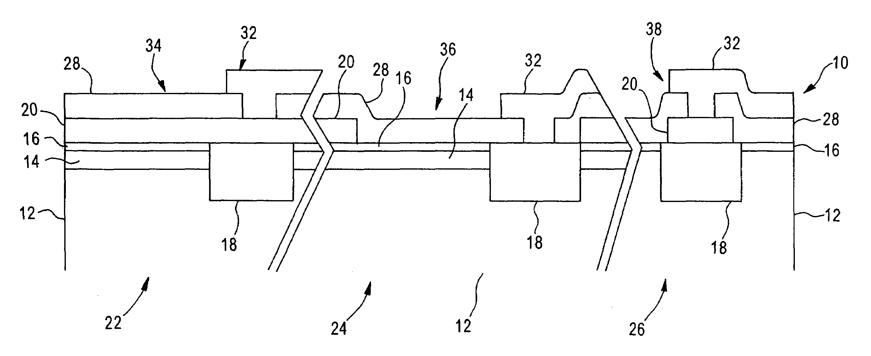
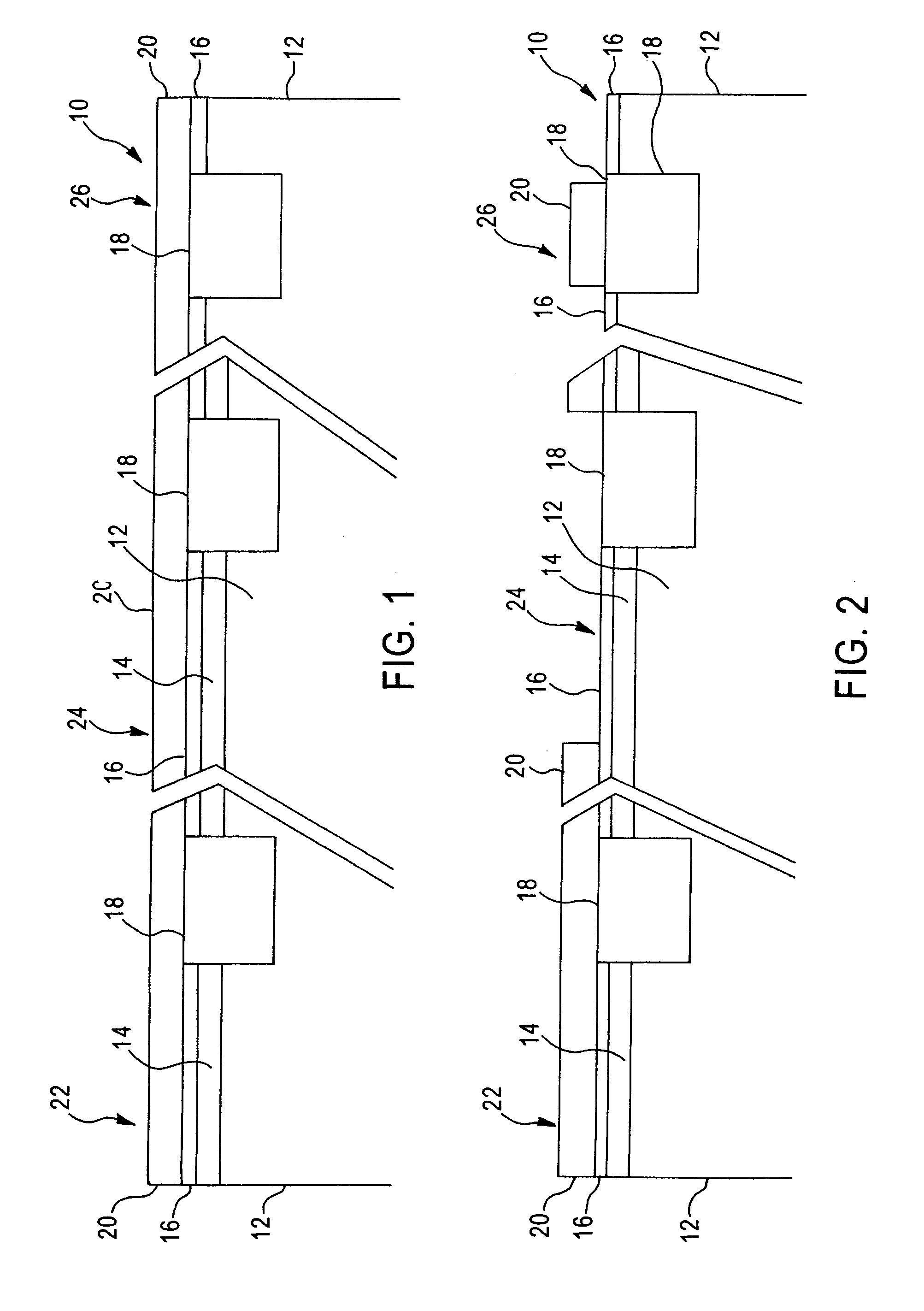
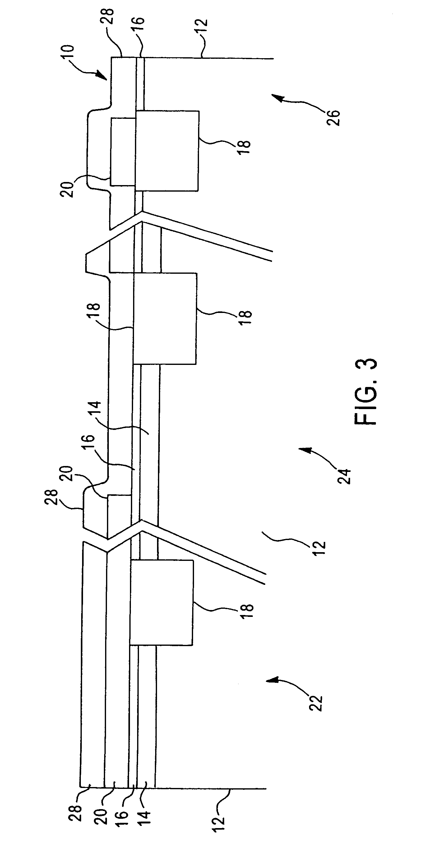
- A semiconductor wafer with internally fabricated stress circuits that apply stress voltages directly to dielectric regions of varying thicknesses, using charge pumps or other voltage converters to generate higher voltages and measure leakage current, thereby assessing dielectric reliability without external influence.


Array of gate dielectric structures to measure gate dielectric thickness and parasitic capacitance
PatentInactiveUS6964875B1
Innovation
- The method involves forming a wafer with gate dielectric capacitors, first dummy structures, and second dummy structures, where the capacitance of the dummy structures is measured and subtracted from the gate dielectric capacitor capacitance to isolate the actual capacitance, allowing for the determination of gate dielectric thickness using the known dielectric constant.

Manufacturing Standards for Printed Electronics Reliability
Manufacturing standards for printed electronics reliability represent a critical framework for ensuring consistent performance and longevity of flexible electronic devices operating at 3.3V. These standards encompass comprehensive guidelines for material selection, process control, and quality assurance protocols specifically tailored to address the unique challenges of printed electronic systems.
The establishment of manufacturing standards begins with substrate preparation requirements, defining acceptable surface roughness parameters, cleanliness levels, and dimensional tolerances. For 3.3V applications, standards specify maximum allowable contamination levels that could compromise dielectric integrity, typically requiring Class 1000 cleanroom conditions during critical processing steps. Temperature and humidity control protocols are mandated to prevent moisture absorption that could lead to premature breakdown.
Process standardization covers printing parameters including ink viscosity ranges, printing speeds, and curing profiles optimized for dielectric layer formation. Standards define acceptable thickness uniformity across printed areas, typically requiring less than 5% variation for reliable voltage withstand capabilities. Layer-to-layer registration accuracy specifications ensure proper device geometry and prevent field concentration effects that could compromise reliability.
Quality control standards incorporate both in-process monitoring and final product testing protocols. Real-time thickness measurement requirements using non-contact methods ensure consistent dielectric properties during production. Electrical testing standards mandate breakdown voltage testing at 150% of operating voltage, with specific test durations and environmental conditions defined to validate long-term reliability performance.
Environmental stress testing standards simulate real-world operating conditions through accelerated aging protocols. These include thermal cycling between -40°C to +85°C, humidity exposure at 85% relative humidity, and mechanical flexing requirements for flexible substrates. Standards specify minimum performance retention levels after standardized stress exposure periods.
Documentation and traceability requirements ensure manufacturing consistency through detailed process records, material lot tracking, and statistical process control implementation. These standards enable continuous improvement and rapid identification of process deviations that could impact device reliability in 3.3V applications.
The establishment of manufacturing standards begins with substrate preparation requirements, defining acceptable surface roughness parameters, cleanliness levels, and dimensional tolerances. For 3.3V applications, standards specify maximum allowable contamination levels that could compromise dielectric integrity, typically requiring Class 1000 cleanroom conditions during critical processing steps. Temperature and humidity control protocols are mandated to prevent moisture absorption that could lead to premature breakdown.
Process standardization covers printing parameters including ink viscosity ranges, printing speeds, and curing profiles optimized for dielectric layer formation. Standards define acceptable thickness uniformity across printed areas, typically requiring less than 5% variation for reliable voltage withstand capabilities. Layer-to-layer registration accuracy specifications ensure proper device geometry and prevent field concentration effects that could compromise reliability.
Quality control standards incorporate both in-process monitoring and final product testing protocols. Real-time thickness measurement requirements using non-contact methods ensure consistent dielectric properties during production. Electrical testing standards mandate breakdown voltage testing at 150% of operating voltage, with specific test durations and environmental conditions defined to validate long-term reliability performance.
Environmental stress testing standards simulate real-world operating conditions through accelerated aging protocols. These include thermal cycling between -40°C to +85°C, humidity exposure at 85% relative humidity, and mechanical flexing requirements for flexible substrates. Standards specify minimum performance retention levels after standardized stress exposure periods.
Documentation and traceability requirements ensure manufacturing consistency through detailed process records, material lot tracking, and statistical process control implementation. These standards enable continuous improvement and rapid identification of process deviations that could impact device reliability in 3.3V applications.
Environmental Impact of Printed Electronics Production
The environmental implications of printed electronics production, particularly in the context of optimizing dielectric thickness for 3.3V reliability applications, present both challenges and opportunities for sustainable manufacturing. Traditional silicon-based electronics manufacturing involves energy-intensive processes, toxic chemicals, and significant waste generation. Printed electronics offer a paradigm shift toward more environmentally conscious production methods through additive manufacturing techniques that minimize material waste and reduce energy consumption.
The production of dielectric materials for printed electronics typically involves solution-based processing at relatively low temperatures, significantly reducing the carbon footprint compared to conventional semiconductor fabrication. Organic and hybrid dielectric materials can be processed at temperatures below 200°C, eliminating the need for high-temperature furnaces that consume substantial energy. This low-temperature processing capability enables the use of flexible plastic substrates, which can be manufactured with lower environmental impact than rigid silicon wafers.
Material selection for dielectric layers plays a crucial role in environmental sustainability. Bio-based polymers and recyclable materials are increasingly being explored as alternatives to traditional petroleum-derived dielectrics. These sustainable materials can maintain the required electrical properties for 3.3V applications while offering end-of-life recyclability. Additionally, the reduced thickness requirements in optimized dielectric designs directly translate to lower material consumption and reduced waste generation.
Solvent usage in printed electronics production represents a significant environmental consideration. Water-based and eco-friendly solvent systems are being developed to replace harmful organic solvents traditionally used in dielectric material preparation. The optimization of dielectric thickness allows for reduced solvent consumption per unit area, further minimizing environmental impact. Advanced printing techniques such as inkjet and screen printing enable precise material deposition, reducing overspray and material waste.
The scalability of printed electronics manufacturing offers potential for distributed production models, reducing transportation-related emissions. Local production capabilities can minimize the carbon footprint associated with global supply chains. Furthermore, the compatibility with roll-to-roll processing enables high-volume production with improved energy efficiency compared to batch processing methods used in conventional electronics manufacturing.
Waste management and recycling considerations are integral to sustainable printed electronics production. The development of biodegradable dielectric materials and recyclable substrate systems addresses end-of-life environmental concerns. Design optimization for 3.3V reliability applications can incorporate circular economy principles, ensuring that materials can be recovered and reused in subsequent manufacturing cycles, thereby reducing the overall environmental burden of electronic device production.
The production of dielectric materials for printed electronics typically involves solution-based processing at relatively low temperatures, significantly reducing the carbon footprint compared to conventional semiconductor fabrication. Organic and hybrid dielectric materials can be processed at temperatures below 200°C, eliminating the need for high-temperature furnaces that consume substantial energy. This low-temperature processing capability enables the use of flexible plastic substrates, which can be manufactured with lower environmental impact than rigid silicon wafers.
Material selection for dielectric layers plays a crucial role in environmental sustainability. Bio-based polymers and recyclable materials are increasingly being explored as alternatives to traditional petroleum-derived dielectrics. These sustainable materials can maintain the required electrical properties for 3.3V applications while offering end-of-life recyclability. Additionally, the reduced thickness requirements in optimized dielectric designs directly translate to lower material consumption and reduced waste generation.
Solvent usage in printed electronics production represents a significant environmental consideration. Water-based and eco-friendly solvent systems are being developed to replace harmful organic solvents traditionally used in dielectric material preparation. The optimization of dielectric thickness allows for reduced solvent consumption per unit area, further minimizing environmental impact. Advanced printing techniques such as inkjet and screen printing enable precise material deposition, reducing overspray and material waste.
The scalability of printed electronics manufacturing offers potential for distributed production models, reducing transportation-related emissions. Local production capabilities can minimize the carbon footprint associated with global supply chains. Furthermore, the compatibility with roll-to-roll processing enables high-volume production with improved energy efficiency compared to batch processing methods used in conventional electronics manufacturing.
Waste management and recycling considerations are integral to sustainable printed electronics production. The development of biodegradable dielectric materials and recyclable substrate systems addresses end-of-life environmental concerns. Design optimization for 3.3V reliability applications can incorporate circular economy principles, ensuring that materials can be recovered and reused in subsequent manufacturing cycles, thereby reducing the overall environmental burden of electronic device production.
Unlock deeper insights with PatSnap Eureka Quick Research — get a full tech report to explore trends and direct your research. Try now!
Generate Your Research Report Instantly with AI Agent
Supercharge your innovation with PatSnap Eureka AI Agent Platform!