Optimizing Field Emission Display using Metalenses Technology
APR 14, 20269 MIN READ
Generate Your Research Report Instantly with AI Agent
Patsnap Eureka helps you evaluate technical feasibility & market potential.
Metalenses FED Technology Background and Objectives
Field Emission Display technology represents a significant advancement in flat panel display systems, combining the benefits of cathode ray tube image quality with the compact form factor of modern displays. FED technology operates on the principle of electron emission from microscopic cathode tips, creating images through phosphor excitation without requiring the bulky electron guns found in traditional CRT displays. This technology emerged in the late 20th century as researchers sought alternatives to liquid crystal displays that could deliver superior contrast ratios, faster response times, and wider viewing angles.
The integration of metalenses technology into FED systems represents a paradigm shift in display optimization approaches. Metalenses, composed of carefully engineered nanostructures arranged in precise patterns, offer unprecedented control over electromagnetic wave propagation at subwavelength scales. These ultra-thin optical elements can manipulate light with remarkable precision, enabling functionalities that traditional refractive optics cannot achieve within comparable size constraints.
The convergence of metalenses and FED technologies addresses several critical limitations inherent in conventional field emission displays. Traditional FED systems often struggle with electron beam focusing accuracy, leading to reduced image sharpness and color uniformity across the display surface. Additionally, conventional focusing mechanisms add complexity and thickness to the overall display assembly, limiting miniaturization potential.
The primary objective of incorporating metalenses into FED systems centers on achieving superior electron beam control and optical performance enhancement. By leveraging the unique electromagnetic manipulation capabilities of metalenses, researchers aim to develop more precise electron focusing mechanisms that can significantly improve pixel-level accuracy and overall image quality. This approach promises to deliver enhanced resolution capabilities while maintaining the inherent advantages of field emission technology.
Furthermore, the metalenses-FED integration seeks to address scalability challenges that have historically limited widespread FED adoption. The objective extends beyond mere performance improvements to encompass manufacturing efficiency and cost reduction through simplified optical architectures. By replacing complex multi-element focusing systems with single metalens structures, the technology aims to streamline production processes while achieving superior optical performance.
The strategic implementation of metalenses technology in FED systems also targets next-generation display applications requiring ultra-high pixel densities and exceptional color accuracy. This technological fusion represents a forward-looking approach to display engineering, positioning FED technology as a viable solution for emerging applications in augmented reality, professional imaging, and high-end consumer electronics markets.
Market Demand for Advanced Display Technologies
The global display technology market is experiencing unprecedented growth driven by increasing consumer demand for high-quality visual experiences across multiple sectors. Traditional display technologies, while established, face significant limitations in meeting emerging requirements for ultra-high resolution, energy efficiency, and compact form factors. This gap has created substantial market opportunities for advanced display solutions that can deliver superior performance characteristics.
Field emission displays represent a promising technology segment within the broader advanced display market, offering unique advantages such as fast response times, wide viewing angles, and excellent brightness uniformity. However, conventional field emission displays have struggled with manufacturing complexity and cost-effectiveness, limiting their commercial adoption. The integration of metalenses technology presents a transformative opportunity to address these fundamental challenges while enhancing overall display performance.
Consumer electronics manufacturers are increasingly seeking display technologies that can support next-generation applications including augmented reality, virtual reality, and ultra-portable devices. These applications demand displays with exceptional optical quality, minimal thickness, and reduced power consumption. The combination of field emission displays with metalenses technology directly addresses these market requirements by enabling precise light control and improved optical efficiency.
The automotive industry represents another significant demand driver, particularly for head-up displays and advanced dashboard systems. Modern vehicles require display technologies that can operate reliably under extreme environmental conditions while providing clear, bright images. Field emission displays enhanced with metalenses technology offer superior performance in high-temperature and high-vibration environments compared to conventional LCD or OLED alternatives.
Enterprise and professional markets are also driving demand for advanced display technologies, particularly in medical imaging, aerospace, and defense applications. These sectors require displays with exceptional color accuracy, high brightness levels, and long operational lifespans. The unique characteristics of metalenses-optimized field emission displays make them particularly suitable for these demanding applications.
Market research indicates strong growth potential for display technologies that can simultaneously improve performance while reducing manufacturing complexity. The convergence of field emission display technology with metalenses represents a strategic opportunity to capture market share in high-value segments where traditional display technologies face performance limitations.
Current FED Limitations and Metalenses Development Status
Field Emission Displays face several critical limitations that have hindered their widespread commercial adoption despite their theoretical advantages over conventional display technologies. The primary challenge lies in achieving uniform electron emission across large display areas, as cathode materials exhibit inherent variations in emission characteristics that result in brightness non-uniformity and pixel-level inconsistencies. Current carbon nanotube and silicon-based cathodes suffer from degradation over time due to ion bombardment and contamination, leading to reduced display lifespan and reliability issues.
Power consumption remains another significant constraint, as FED systems require high voltage operations typically ranging from 1-10 kV to achieve sufficient electron emission. This high voltage requirement not only increases energy consumption but also introduces safety concerns and necessitates complex power management circuits. Additionally, the vacuum packaging requirements for FED technology present manufacturing challenges, including maintaining ultra-high vacuum levels and preventing outgassing from internal components that can poison the cathode surface.
Manufacturing scalability represents a substantial barrier, particularly in achieving cost-effective production of large-area displays. The precision required for cathode patterning and the need for specialized vacuum processing equipment significantly increase production costs compared to established LCD and OLED technologies. Quality control becomes increasingly difficult as display sizes increase, with yield rates often falling below commercially viable thresholds.
Metalenses technology has emerged as a promising optical manipulation solution, leveraging metasurfaces composed of subwavelength nanostructures to control electromagnetic waves with unprecedented precision. Recent developments in metalenses have demonstrated remarkable capabilities in beam focusing, steering, and wavefront shaping across various spectral ranges. Silicon-based metalenses operating in the visible spectrum have achieved numerical apertures exceeding 0.9 with focusing efficiencies above 80%, representing significant progress from early proof-of-concept demonstrations.
Current metalenses fabrication relies primarily on electron beam lithography and advanced photolithography techniques, enabling feature sizes down to 50 nanometers with high aspect ratios. Titanium dioxide, gallium nitride, and silicon nitride have emerged as preferred materials due to their high refractive indices and low optical losses. Multi-layer metalenses designs have successfully addressed chromatic aberration issues, achieving broadband operation across 400-700 nm wavelength ranges.
The integration potential between FED and metalenses technologies presents unique opportunities for addressing electron beam control and focusing challenges. Metalenses could potentially replace bulky electromagnetic focusing systems currently used in FED architectures, offering compact, lightweight alternatives with superior beam shaping capabilities. However, adaptation challenges exist in scaling metalenses designs for electron beam applications, as most current developments focus on photonic rather than electronic applications.
Current Metalenses Integration Solutions for FED
01 Electron emission source structures and materials
Field emission displays utilize specialized electron emission sources with specific structural configurations and materials to enhance emission efficiency. These structures include carbon-based materials, nanomaterials, and specially designed cathode configurations that improve electron emission characteristics. The emission sources are engineered to provide stable and uniform electron emission across the display surface, which is critical for image quality and display performance.- Electron emission source structures and materials: Field emission displays utilize specialized electron emission sources with specific structural configurations and materials to enhance emission efficiency. These structures include carbon-based materials, nanomaterials, and specially designed cathode configurations that improve electron emission characteristics. The emission sources are engineered to provide stable and uniform electron emission across the display surface, which is critical for image quality and display performance.
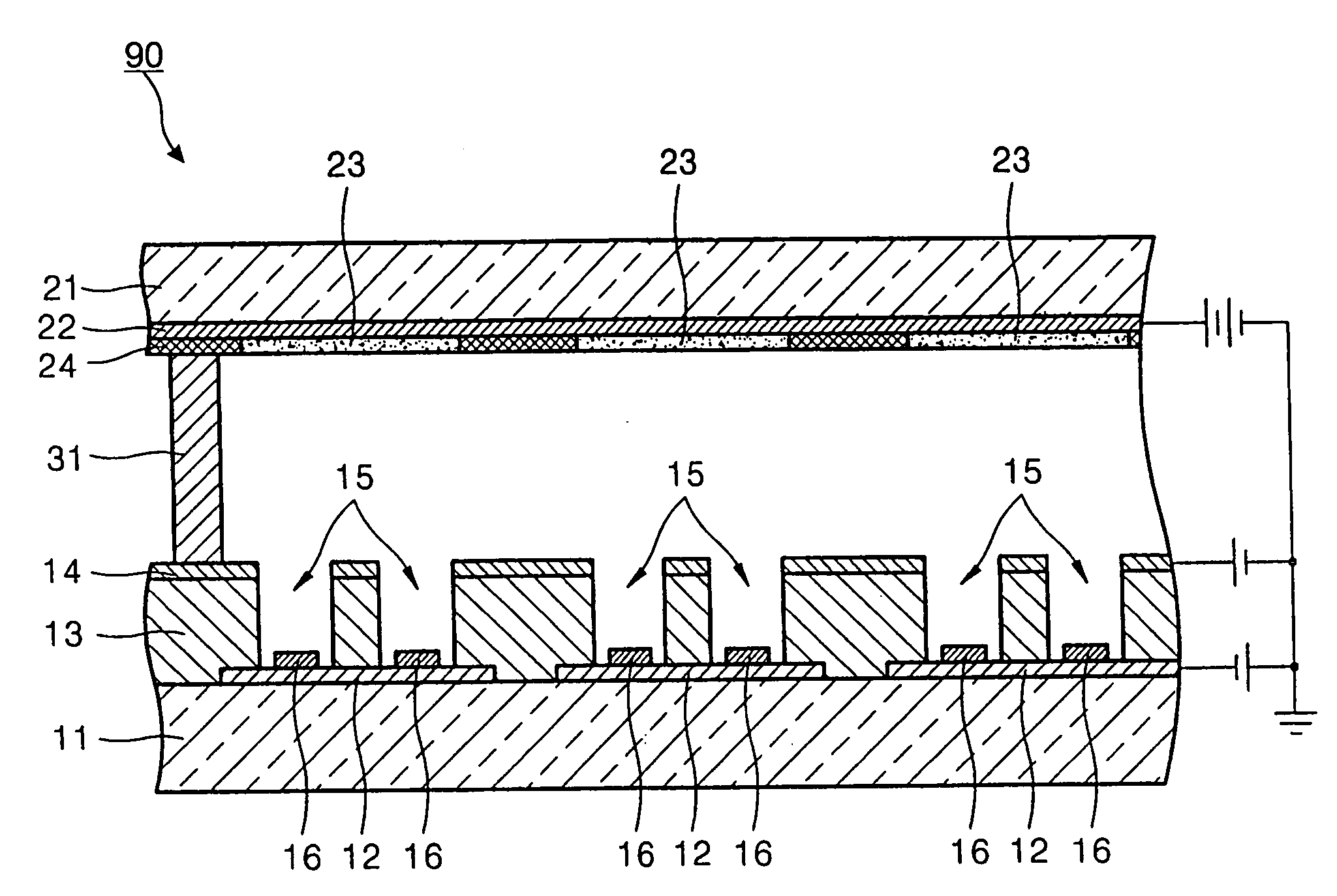
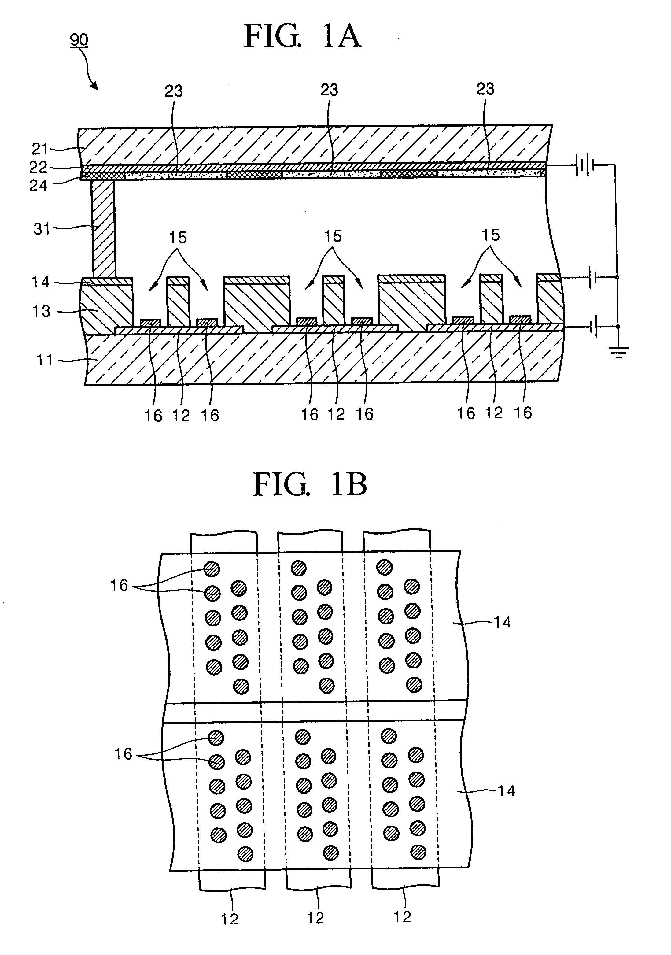
- Gate electrode and extraction electrode designs: The gate electrode structure plays a crucial role in controlling electron emission in field emission displays. Various designs focus on optimizing the gate electrode configuration, spacing, and materials to improve extraction efficiency and reduce operating voltage. These designs include specific geometric patterns, multi-layer structures, and novel fabrication methods that enhance the electric field distribution and electron extraction capabilities.
- Spacer structures and vacuum sealing technologies: Maintaining proper spacing between the cathode and anode plates while ensuring vacuum integrity is essential for field emission display operation. Spacer structures are designed to provide mechanical support, prevent electrical breakdown, and maintain uniform gap distances. Advanced sealing technologies ensure long-term vacuum stability and prevent contamination that could degrade emission performance.
- Phosphor screen and anode plate configurations: The phosphor screen and anode plate assembly converts electron beams into visible light in field emission displays. Innovations include optimized phosphor materials, screen patterning techniques, and anode structures that improve light emission efficiency, color purity, and brightness uniformity. These configurations also address issues related to charging effects and screen degradation over time.
- Drive circuits and control methods: Effective driving and control systems are necessary to operate field emission displays with proper addressing, brightness control, and image rendering. These systems include specialized driver circuits, voltage regulation methods, and addressing schemes that enable matrix operation of the display. Advanced control methods optimize power consumption, improve response time, and ensure uniform brightness across the display area.
02 Gate electrode and extraction electrode designs
The gate electrode structure plays a crucial role in controlling electron emission in field emission displays. Various designs focus on optimizing the gate electrode geometry, spacing, and materials to improve extraction efficiency and reduce operating voltage. These designs include specific aperture configurations, multi-layer electrode structures, and novel fabrication methods that enhance the electric field distribution for better electron extraction and beam focusing.Expand Specific Solutions03 Spacer structures and vacuum sealing technologies
Maintaining proper spacing between the cathode and anode plates while ensuring vacuum integrity is essential for field emission display operation. Spacer structures are designed to provide mechanical support, prevent electrical breakdown, and maintain uniform gap distances. Advanced vacuum sealing technologies and getter materials are employed to maintain the required vacuum level throughout the display lifetime, preventing contamination and ensuring stable operation.Expand Specific Solutions04 Phosphor screen and light emission optimization
The phosphor screen configuration and composition are optimized to convert electron bombardment into visible light efficiently. Various phosphor materials and deposition techniques are employed to achieve high brightness, color purity, and long operational lifetime. The screen structure includes considerations for electron energy distribution, phosphor particle size, and protective layers to enhance luminous efficiency and prevent degradation.Expand Specific Solutions05 Driving circuits and control methods
Specialized driving circuits and control methods are developed to address the unique requirements of field emission displays. These include voltage regulation systems, scanning control circuits, and addressing schemes that enable precise control of individual pixels or pixel groups. The driving methods focus on reducing power consumption, improving response time, and ensuring uniform brightness across the display while managing the high voltages required for electron emission.Expand Specific Solutions
Key Players in FED and Metalenses Industry
The field emission display optimization using metalenses technology represents an emerging convergence at the intersection of advanced display systems and metamaterial optics, currently in its early commercialization phase. The market demonstrates significant growth potential as traditional display manufacturers like Samsung Display, LG Electronics, and BOE Technology Group explore next-generation solutions beyond conventional LCD and OLED technologies. Technology maturity varies considerably across stakeholders, with established display giants Samsung SDI and Innolux possessing strong manufacturing capabilities, while specialized firms like Shenzhen Metalance Technology focus specifically on metalens development. Research institutions including Tsinghua University and Harvard College drive fundamental innovations, though practical implementation remains challenging. The competitive landscape shows fragmentation between traditional electronics manufacturers (Canon, Mitsubishi Electric, Huawei) leveraging existing optical expertise and emerging players developing metamaterial solutions, indicating the technology is transitioning from laboratory research toward industrial applications but requires further development for mass market viability.
Hon Hai Precision Industry Co., Ltd.
Technical Solution: Hon Hai Precision has developed manufacturing processes for metalens-enhanced field emission displays focusing on scalable production techniques. Their approach emphasizes the integration of metalens fabrication into existing display manufacturing workflows, utilizing advanced lithography and etching processes to create precise nanostructures on field emission cathode arrays. The company has developed specialized coating techniques that allow metalenses to be directly integrated onto field emission tips, improving electron beam shaping and reducing aberrations. Their technology platform includes automated inspection systems for quality control of metalens structures and optimized assembly processes that maintain the precise alignment required between metalens arrays and field emission cathodes for optimal display performance.
Strengths: Strong manufacturing expertise, cost-effective production capabilities, established supply chain networks. Weaknesses: Limited fundamental research capabilities, dependence on technology partnerships for advanced innovations.
Samsung Display Co., Ltd.
Technical Solution: Samsung Display has developed advanced metalens-integrated field emission display technology that utilizes nanostructured metasurfaces to enhance electron beam focusing and control. Their approach combines traditional field emission cathodes with precisely engineered metalens arrays that can manipulate the electron beam trajectory and improve emission uniformity across the display panel. The technology incorporates phase-gradient metasurfaces positioned strategically within the display architecture to achieve better beam collimation and reduced crosstalk between adjacent pixels. This integration allows for higher resolution displays with improved brightness uniformity and enhanced viewing angles while maintaining the fast response times characteristic of field emission displays.
Strengths: Market leadership in display technology, extensive manufacturing capabilities, strong R&D resources. Weaknesses: High manufacturing complexity, potential cost challenges for mass production.
Core Patents in Metalenses-Enhanced FED Systems
Metalens collimators and condensers
PatentActiveUS20240151983A1
Innovation
- The development of metalenses with subwavelength-scale pillars and interelement spacings, made from materials like titanium dioxide or polysilicon, which are thinner, more efficient, and capable of modifying the emission profile of LEDs to achieve focused, collimated, or concentrated optical radiation with high transmission efficiency.


Field emission display having an improved emitter structure
PatentInactiveUS20080290782A1
Innovation
- The design of an improved FED with a cathode electrode structure featuring conductive and insulation layers, apertures, and carbon-based emitters, such as carbon nano-tubes, that are strategically positioned to enhance electron beam focusing and reduce dispersion, using cavities and specific aperture configurations to optimize electric field distribution and emitter placement.

Manufacturing Scalability Challenges for Metalenses FED
The manufacturing scalability of metalenses for field emission displays presents significant challenges that must be addressed to achieve commercial viability. Current fabrication methods rely heavily on electron beam lithography and focused ion beam techniques, which offer exceptional precision but are inherently slow and expensive for large-scale production. These serial writing processes become increasingly impractical when scaling to display panel dimensions, where millions of metalens elements must be fabricated with nanometer-scale accuracy.
Photolithography-based approaches show promise for addressing throughput limitations, but face substantial technical hurdles. The sub-wavelength features required for metalenses operating in visible and near-infrared spectra push conventional photolithography to its limits. Deep ultraviolet and extreme ultraviolet lithography systems can achieve the necessary resolution, but their high capital costs and complex operational requirements create significant barriers to widespread adoption. Additionally, the aspect ratios required for efficient metalens structures often exceed what can be reliably achieved through standard photolithographic processes.
Nanoimprint lithography emerges as a potentially viable solution for high-volume manufacturing, offering the ability to replicate complex nanostructures across large areas simultaneously. However, this approach faces challenges in maintaining uniform pressure distribution across display-sized substrates and ensuring defect-free pattern transfer. The durability of imprint templates under repeated use and the development of suitable resist materials for metalens fabrication remain active areas of research.
Material deposition and etching processes present additional scalability concerns. Achieving uniform thickness control of high-index dielectric materials across large substrates while maintaining the optical properties required for metalens functionality requires sophisticated process control. Plasma etching processes must deliver consistent anisotropic profiles across the entire substrate area, with variations in etch rate potentially compromising metalens performance.
Quality control and metrology at manufacturing scale pose unprecedented challenges. Traditional optical inspection methods lack the resolution needed to verify individual metalens elements, while high-resolution techniques like scanning electron microscopy are too slow for production environments. Development of rapid, non-destructive characterization methods capable of assessing metalens performance across large areas remains a critical need for manufacturing scalability.
Optical Performance Optimization Strategies
The optimization of optical performance in field emission displays utilizing metalenses technology requires a comprehensive approach addressing multiple critical parameters. The primary focus centers on enhancing light extraction efficiency, improving beam collimation, and achieving superior color uniformity across the display surface. These objectives demand careful consideration of metalens design parameters, including nanostructure geometry, material selection, and spatial arrangement to maximize photonic efficiency while minimizing optical losses.
Wavelength-specific optimization represents a fundamental strategy for achieving enhanced optical performance. Metalenses can be engineered with wavelength-dependent phase profiles to provide optimal focusing characteristics for red, green, and blue emission wavelengths. This approach involves designing subwavelength nanostructures with precise geometric parameters that create constructive interference patterns for specific wavelengths while maintaining acceptable performance across the visible spectrum. Advanced computational modeling techniques enable the prediction and optimization of these wavelength-dependent responses.
Beam shaping and collimation strategies play crucial roles in improving display brightness and viewing angle characteristics. Metalenses can be designed to transform the typically Lambertian emission pattern of field emission sources into more directional beams, thereby increasing luminous efficiency in the forward direction. This involves implementing phase gradient designs that redirect off-axis light toward the normal viewing direction, effectively concentrating the optical power within desired angular ranges.
Polarization management emerges as another critical optimization avenue, particularly for displays requiring specific polarization states for enhanced contrast or compatibility with external optical components. Metalenses can incorporate polarization-selective elements that simultaneously focus light and control polarization states, eliminating the need for additional polarizing components that introduce optical losses.
Spatial uniformity optimization addresses the challenge of maintaining consistent optical performance across large display areas. This involves developing metalens arrays with position-dependent designs that compensate for variations in field emission characteristics and ensure uniform brightness and color reproduction. Advanced fabrication techniques enable the creation of spatially varying metalens parameters to achieve this uniformity.
Integration strategies focus on seamlessly incorporating metalenses into existing field emission display architectures while maintaining manufacturing feasibility and cost-effectiveness. This includes optimizing the metalens substrate materials, thickness constraints, and alignment tolerances to ensure reliable performance under operational conditions while facilitating scalable production processes.
Unlock deeper insights with Patsnap Eureka Quick Research — get a full tech report to explore trends and direct your research. Try now!
Generate Your Research Report Instantly with AI Agent
Supercharge your innovation with Patsnap Eureka AI Agent Platform!