

Optimizing Read Paths for Low-Powered Devices Using Ferroelectric RAM
MAY 14, 20269 MIN READ
Generate Your Research Report Instantly with AI Agent
PatSnap Eureka helps you evaluate technical feasibility & market potential.
FeRAM Read Path Optimization Background and Objectives
Ferroelectric Random Access Memory (FeRAM) has emerged as a critical technology in the evolution of non-volatile memory solutions, particularly for applications requiring ultra-low power consumption. The fundamental principle of FeRAM relies on ferroelectric materials that exhibit spontaneous electric polarization, which can be reversed by applying an external electric field. This unique characteristic enables data retention without continuous power supply while maintaining fast read and write operations comparable to traditional SRAM.
The historical development of FeRAM technology traces back to the 1950s when ferroelectric materials were first discovered for memory applications. However, practical implementation remained challenging until the 1990s when advances in thin-film deposition techniques and material science enabled commercial viability. The technology has since evolved through several generations, with improvements in cell scaling, endurance, and integration density.
Current market demands for low-powered devices have intensified the focus on optimizing FeRAM read path operations. The proliferation of Internet of Things (IoT) devices, wearable electronics, and battery-powered sensors has created an urgent need for memory solutions that can operate efficiently under strict power constraints. Traditional memory technologies often consume excessive power during read operations, limiting battery life and overall system performance.
The primary technical objective of FeRAM read path optimization centers on minimizing power consumption while maintaining data integrity and access speed. This involves reducing parasitic capacitances, optimizing sense amplifier designs, and implementing advanced voltage scaling techniques. The challenge lies in balancing these competing requirements while ensuring reliable operation across varying environmental conditions.
Key performance targets include achieving read currents below 10 microamperes, reducing read access times to sub-100 nanoseconds, and maintaining data retention for over 10 years at operating temperatures up to 85 degrees Celsius. Additionally, the optimization must address process variations and aging effects that can impact long-term reliability.
The strategic importance of this technology extends beyond immediate power savings, as it enables new applications in energy harvesting systems, medical implants, and autonomous sensor networks where power efficiency directly correlates with system viability and operational lifetime.
The historical development of FeRAM technology traces back to the 1950s when ferroelectric materials were first discovered for memory applications. However, practical implementation remained challenging until the 1990s when advances in thin-film deposition techniques and material science enabled commercial viability. The technology has since evolved through several generations, with improvements in cell scaling, endurance, and integration density.
Current market demands for low-powered devices have intensified the focus on optimizing FeRAM read path operations. The proliferation of Internet of Things (IoT) devices, wearable electronics, and battery-powered sensors has created an urgent need for memory solutions that can operate efficiently under strict power constraints. Traditional memory technologies often consume excessive power during read operations, limiting battery life and overall system performance.
The primary technical objective of FeRAM read path optimization centers on minimizing power consumption while maintaining data integrity and access speed. This involves reducing parasitic capacitances, optimizing sense amplifier designs, and implementing advanced voltage scaling techniques. The challenge lies in balancing these competing requirements while ensuring reliable operation across varying environmental conditions.
Key performance targets include achieving read currents below 10 microamperes, reducing read access times to sub-100 nanoseconds, and maintaining data retention for over 10 years at operating temperatures up to 85 degrees Celsius. Additionally, the optimization must address process variations and aging effects that can impact long-term reliability.
The strategic importance of this technology extends beyond immediate power savings, as it enables new applications in energy harvesting systems, medical implants, and autonomous sensor networks where power efficiency directly correlates with system viability and operational lifetime.
Market Demand for Low-Power Memory Solutions
The global memory market is experiencing unprecedented demand for low-power solutions, driven by the exponential growth of battery-powered devices and energy-conscious computing applications. Internet of Things devices, wearable technology, and edge computing systems represent the fastest-growing segments requiring memory solutions that can operate efficiently under strict power constraints while maintaining high performance standards.
Mobile computing continues to dominate market demand, with smartphones, tablets, and laptops requiring memory technologies that extend battery life without compromising user experience. The proliferation of always-on devices and ambient computing applications has created a substantial market for non-volatile memory solutions that can retain data without continuous power consumption, making ferroelectric RAM particularly attractive for these applications.
Industrial automation and smart manufacturing sectors are increasingly adopting low-power memory solutions to support distributed sensor networks and autonomous systems. These applications require memory technologies capable of withstanding harsh environmental conditions while maintaining ultra-low power consumption during extended operational periods. The automotive industry represents another significant growth driver, with electric vehicles and advanced driver assistance systems demanding memory solutions that minimize power drain on vehicle batteries.
Healthcare and medical device markets show strong demand for low-power memory technologies, particularly in implantable devices, continuous monitoring systems, and portable diagnostic equipment. These applications require memory solutions that can operate reliably for years without battery replacement while maintaining strict safety and reliability standards.
The enterprise data center market is experiencing growing pressure to reduce energy consumption and operational costs, creating demand for memory technologies that can significantly lower power requirements during read operations. Cloud service providers and hyperscale data centers are actively seeking memory solutions that can reduce their overall energy footprint while maintaining high-performance computing capabilities.
Emerging applications in augmented reality, virtual reality, and mixed reality devices require memory solutions that balance high bandwidth requirements with stringent power constraints to enable portable, untethered user experiences. The growing adoption of artificial intelligence at the edge further amplifies demand for memory technologies that can support intensive computational workloads while operating within the power limitations of battery-powered devices.
Geographic market analysis reveals particularly strong demand growth in Asia-Pacific regions, where consumer electronics manufacturing and adoption rates continue to accelerate, alongside increasing focus on energy efficiency and sustainability across all technology sectors.
Mobile computing continues to dominate market demand, with smartphones, tablets, and laptops requiring memory technologies that extend battery life without compromising user experience. The proliferation of always-on devices and ambient computing applications has created a substantial market for non-volatile memory solutions that can retain data without continuous power consumption, making ferroelectric RAM particularly attractive for these applications.
Industrial automation and smart manufacturing sectors are increasingly adopting low-power memory solutions to support distributed sensor networks and autonomous systems. These applications require memory technologies capable of withstanding harsh environmental conditions while maintaining ultra-low power consumption during extended operational periods. The automotive industry represents another significant growth driver, with electric vehicles and advanced driver assistance systems demanding memory solutions that minimize power drain on vehicle batteries.
Healthcare and medical device markets show strong demand for low-power memory technologies, particularly in implantable devices, continuous monitoring systems, and portable diagnostic equipment. These applications require memory solutions that can operate reliably for years without battery replacement while maintaining strict safety and reliability standards.
The enterprise data center market is experiencing growing pressure to reduce energy consumption and operational costs, creating demand for memory technologies that can significantly lower power requirements during read operations. Cloud service providers and hyperscale data centers are actively seeking memory solutions that can reduce their overall energy footprint while maintaining high-performance computing capabilities.
Emerging applications in augmented reality, virtual reality, and mixed reality devices require memory solutions that balance high bandwidth requirements with stringent power constraints to enable portable, untethered user experiences. The growing adoption of artificial intelligence at the edge further amplifies demand for memory technologies that can support intensive computational workloads while operating within the power limitations of battery-powered devices.
Geographic market analysis reveals particularly strong demand growth in Asia-Pacific regions, where consumer electronics manufacturing and adoption rates continue to accelerate, alongside increasing focus on energy efficiency and sustainability across all technology sectors.
Current FeRAM Read Path Limitations and Power Challenges
Ferroelectric RAM technology faces significant read path limitations that directly impact its adoption in low-powered device applications. The fundamental challenge stems from the destructive read operation inherent to FeRAM cells, where reading data requires applying a voltage that potentially alters the stored ferroelectric polarization state. This destructive nature necessitates immediate write-back operations to restore the original data, effectively doubling the power consumption for each read cycle compared to non-volatile memories with non-destructive read mechanisms.
Current FeRAM architectures exhibit substantial power overhead during sense amplifier operations. The sensing process requires precise voltage discrimination between polarization states, demanding high-gain amplifiers that consume considerable static and dynamic power. These amplifiers must operate within tight timing constraints to distinguish between the relatively small signal differences generated by ferroelectric capacitors, typically ranging from 50-200mV. The power consumption becomes particularly problematic when multiple bitlines are accessed simultaneously, as each requires dedicated sensing circuitry.
The read path timing constraints present another critical limitation affecting power efficiency. FeRAM cells require specific pulse widths and rise times to ensure reliable polarization switching during read operations. These timing requirements often force the memory controller to operate at suboptimal frequencies, leading to increased active power consumption per bit accessed. Additionally, the need for precise timing control necessitates complex clock generation and distribution networks that contribute additional power overhead.
Voltage scaling challenges further compound the power limitations in FeRAM read paths. Unlike conventional CMOS logic that benefits from aggressive voltage scaling, ferroelectric materials require minimum threshold voltages to achieve reliable polarization switching. This constraint limits the effectiveness of traditional low-power design techniques such as dynamic voltage scaling, particularly problematic for battery-operated devices requiring extended operational lifetimes.
The peripheral circuitry supporting FeRAM read operations introduces significant power penalties. Row decoders, column multiplexers, and reference voltage generators must maintain stable operation across process, voltage, and temperature variations while supporting the specific electrical characteristics of ferroelectric capacitors. These circuits typically consume 30-40% of total memory power, representing a substantial overhead for small-capacity implementations common in low-powered applications.
Temperature sensitivity of ferroelectric materials creates additional power management challenges in read path design. The coercive voltage and switching characteristics of ferroelectric capacitors vary significantly with temperature, requiring adaptive biasing schemes and compensation circuits that increase overall power consumption. These thermal dependencies necessitate more robust sensing margins, further increasing the power requirements for reliable read operations in portable device environments.
Current FeRAM architectures exhibit substantial power overhead during sense amplifier operations. The sensing process requires precise voltage discrimination between polarization states, demanding high-gain amplifiers that consume considerable static and dynamic power. These amplifiers must operate within tight timing constraints to distinguish between the relatively small signal differences generated by ferroelectric capacitors, typically ranging from 50-200mV. The power consumption becomes particularly problematic when multiple bitlines are accessed simultaneously, as each requires dedicated sensing circuitry.
The read path timing constraints present another critical limitation affecting power efficiency. FeRAM cells require specific pulse widths and rise times to ensure reliable polarization switching during read operations. These timing requirements often force the memory controller to operate at suboptimal frequencies, leading to increased active power consumption per bit accessed. Additionally, the need for precise timing control necessitates complex clock generation and distribution networks that contribute additional power overhead.
Voltage scaling challenges further compound the power limitations in FeRAM read paths. Unlike conventional CMOS logic that benefits from aggressive voltage scaling, ferroelectric materials require minimum threshold voltages to achieve reliable polarization switching. This constraint limits the effectiveness of traditional low-power design techniques such as dynamic voltage scaling, particularly problematic for battery-operated devices requiring extended operational lifetimes.
The peripheral circuitry supporting FeRAM read operations introduces significant power penalties. Row decoders, column multiplexers, and reference voltage generators must maintain stable operation across process, voltage, and temperature variations while supporting the specific electrical characteristics of ferroelectric capacitors. These circuits typically consume 30-40% of total memory power, representing a substantial overhead for small-capacity implementations common in low-powered applications.
Temperature sensitivity of ferroelectric materials creates additional power management challenges in read path design. The coercive voltage and switching characteristics of ferroelectric capacitors vary significantly with temperature, requiring adaptive biasing schemes and compensation circuits that increase overall power consumption. These thermal dependencies necessitate more robust sensing margins, further increasing the power requirements for reliable read operations in portable device environments.
Existing FeRAM Read Path Optimization Solutions
01 Ferroelectric memory cell read circuit architectures
Various circuit architectures are employed for reading data from ferroelectric memory cells, including differential sensing circuits, reference voltage generation circuits, and specialized amplification stages. These architectures are designed to detect the polarization state of ferroelectric capacitors by measuring charge displacement or voltage changes during read operations. The circuits typically incorporate sense amplifiers, voltage comparators, and timing control mechanisms to ensure accurate data retrieval.- Ferroelectric memory cell read circuit architectures: Various circuit architectures are employed for reading ferroelectric memory cells, including differential sensing circuits and reference cell configurations. These architectures utilize specialized amplifiers and voltage comparators to detect the polarization state of ferroelectric capacitors during read operations. The circuits are designed to minimize noise and maximize signal integrity while maintaining fast access times.
- Non-destructive read methods for ferroelectric memory: Advanced techniques for reading ferroelectric memory without destroying the stored data involve specialized voltage application sequences and sensing methodologies. These methods preserve the ferroelectric polarization state during read operations, eliminating the need for data restoration cycles and improving memory endurance. The approaches often utilize partial switching or low-voltage sensing techniques.
- Sense amplifier designs for ferroelectric RAM: Specialized sense amplifier circuits are crucial for detecting small voltage differences generated by ferroelectric capacitors during read operations. These amplifiers feature high sensitivity, low offset voltage, and fast response times to accurately distinguish between logic states. The designs often incorporate differential input stages and noise reduction techniques to enhance signal detection reliability.
- Reference voltage generation and calibration systems: Accurate reference voltage generation is essential for reliable ferroelectric memory read operations. These systems provide stable voltage references that serve as comparison points for determining the stored data state. Calibration mechanisms ensure optimal reference levels across process variations, temperature changes, and aging effects to maintain consistent read margins throughout the memory's operational lifetime.
- Read path timing and control mechanisms: Precise timing control is critical for ferroelectric memory read operations to ensure proper data sensing and signal development. Control circuits manage the sequence of operations including precharge phases, sense enable timing, and data output synchronization. These mechanisms coordinate multiple circuit blocks to optimize read speed while maintaining data integrity and preventing read disturb effects.
02 Non-destructive read methods and techniques
Advanced techniques for performing non-destructive read operations in ferroelectric memory devices focus on preserving the stored data while accessing it. These methods involve careful voltage control, pulse timing optimization, and specialized sensing schemes that minimize disturbance to the ferroelectric polarization state. The approaches include partial switching detection, charge integration methods, and multi-level sensing capabilities.Expand Specific Solutions03 Reference signal generation for ferroelectric memory reading
Reference signal generation systems provide stable comparison voltages or currents for accurate data detection in ferroelectric memory arrays. These systems include reference cell arrays, dummy cell structures, and calibration circuits that compensate for process variations and environmental factors. The reference generation methods ensure consistent read margins and improve reliability across different operating conditions.Expand Specific Solutions04 Sense amplifier designs for ferroelectric RAM
Specialized sense amplifier configurations are developed to handle the unique characteristics of ferroelectric memory cells, including their charge-based switching behavior and timing requirements. These amplifiers feature high sensitivity, fast response times, and noise immunity to accurately distinguish between different polarization states. The designs incorporate differential input stages, offset compensation, and adaptive biasing schemes.Expand Specific Solutions05 Read path optimization and timing control
Optimization techniques for ferroelectric memory read paths focus on minimizing access time, reducing power consumption, and improving signal integrity. These approaches include advanced timing control circuits, pipeline architectures, and signal conditioning methods. The optimization strategies address issues such as parasitic capacitance effects, voltage settling times, and cross-talk between adjacent memory cells.Expand Specific Solutions
Key Players in FeRAM and Low-Power Memory Industry
The ferroelectric RAM (FeRAM) optimization landscape for low-powered devices represents a mature yet evolving market segment within the broader non-volatile memory industry. The technology has progressed beyond early research phases, with established semiconductor giants like Samsung Electronics, Toshiba, and Texas Instruments leading commercial implementations alongside specialized players such as ROHM and LAPIS Semiconductor. The competitive environment spans from foundry leaders like Taiwan Semiconductor Manufacturing Company providing manufacturing capabilities to emerging focused companies like RAMXEED and Shanghai Ciyu Information Technologies driving innovation in next-generation memory architectures. Research institutions including Forschungszentrum Jülich, CEA, and various universities continue advancing fundamental FeRAM technologies, while the market shows strong growth potential driven by IoT, automotive, and industrial applications requiring ultra-low power consumption and high endurance characteristics.
Samsung Electronics Co., Ltd.
Technical Solution: Samsung has developed advanced ferroelectric RAM (FeRAM) solutions optimized for low-power applications, incorporating proprietary ferroelectric materials and memory cell architectures. Their FeRAM technology features ultra-low standby current consumption below 1μA and fast write/read cycles under 100ns, making it ideal for battery-powered IoT devices. The company has implemented specialized read path optimization techniques including adaptive voltage scaling and intelligent power gating to minimize energy consumption during data access operations. Samsung's FeRAM solutions support wide operating voltage ranges from 1.8V to 5.5V and maintain data retention for over 10 years without power, significantly extending battery life in portable devices.
Strengths: Market-leading manufacturing capabilities, extensive R&D resources, proven track record in memory technologies. Weaknesses: Higher cost compared to traditional memory solutions, limited density scalability for high-capacity applications.
Texas Instruments Incorporated
Technical Solution: Texas Instruments has pioneered FeRAM technology with their MSP430 microcontroller series featuring integrated ferroelectric memory for ultra-low-power applications. Their approach focuses on optimizing read paths through hardware-software co-design, implementing intelligent memory access patterns and dynamic power management. TI's FeRAM solutions achieve standby currents as low as 0.1μA while maintaining instant-on capability and eliminating the need for battery backup. The company has developed specialized compiler optimizations and memory mapping techniques that reduce read access energy by up to 50% compared to conventional approaches. Their integrated solutions combine FeRAM with ultra-low-power processing cores, enabling complete system-on-chip implementations for energy-harvesting applications.
Strengths: Deep expertise in low-power design, comprehensive ecosystem support, strong market presence in embedded systems. Weaknesses: Limited to lower-density applications, dependency on proprietary toolchains and development environments.
Core Patents in FeRAM Read Circuit Design
Ferroelectric random access memory device and method for operating read and write thereof
PatentActiveUS20220215870A1
Innovation
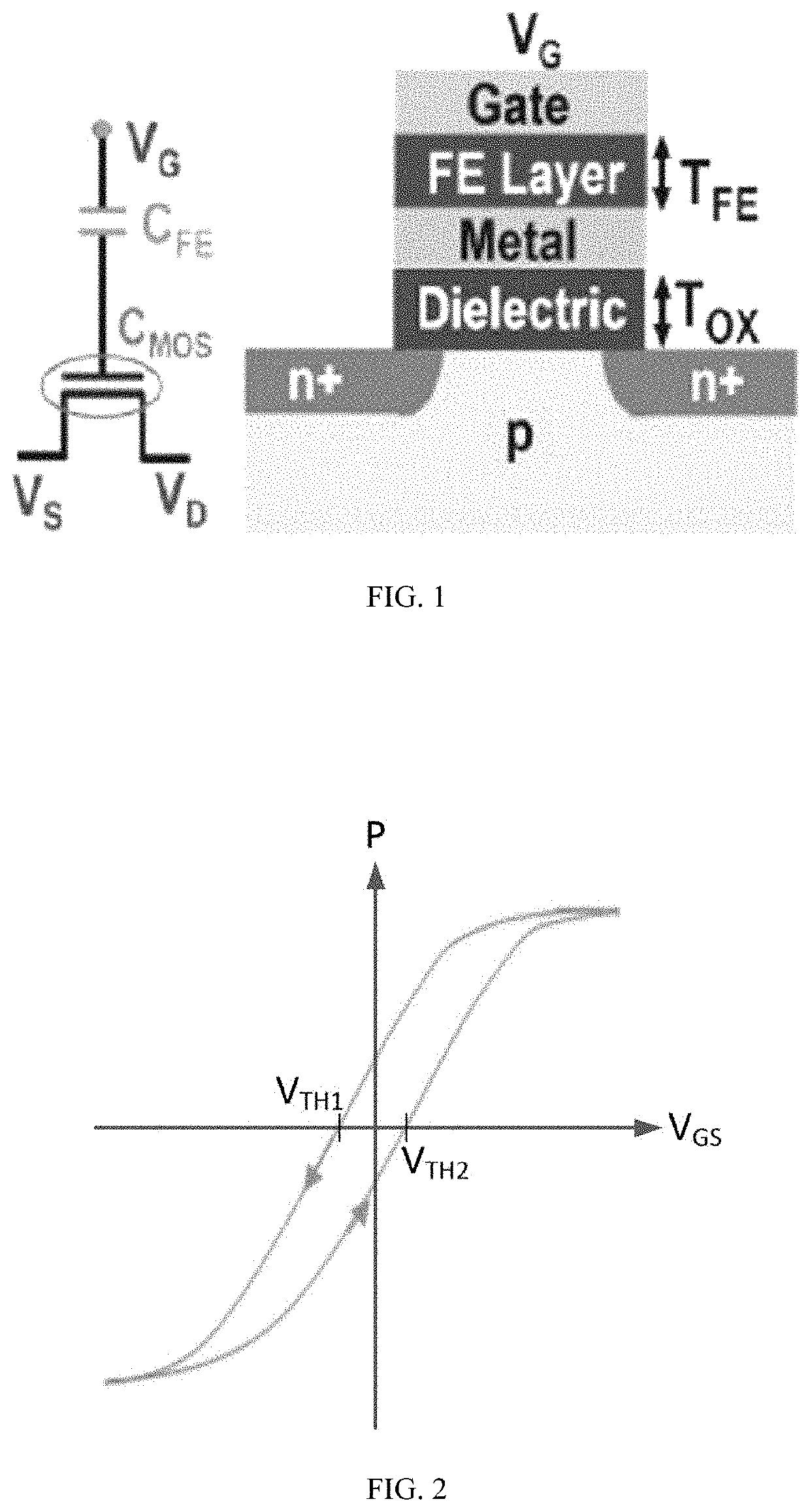
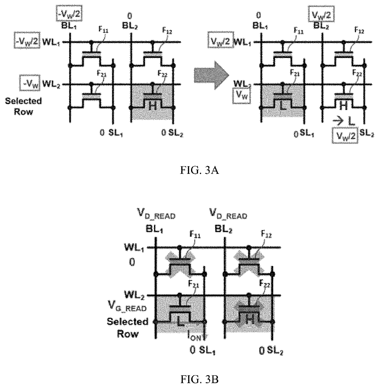
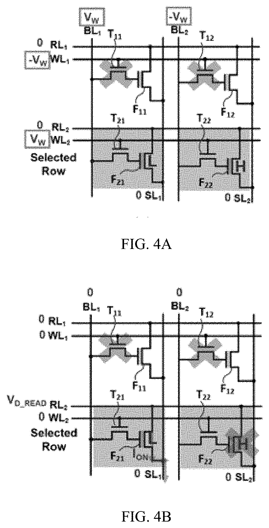
- A ferroelectric random access memory device with a memory cell array and a read/write control unit that applies a positive write voltage to selected word and read lines, eliminating the need for negative voltages and reducing power consumption by shifting the hysteresis curve of the FeFET in the positive voltage direction, allowing data to be written and read using fewer voltage levels.

Chain ferroelectric random access memory (CFRAM) having an intrinsic transistor connected in parallel with a ferroelectric capacitor
PatentInactiveUS7295456B2
Innovation
- The implementation of a memory cell unit with serially connected ferroelectric capacitors and MOS transistors, where the gate voltage of a second MOS transistor is controlled to maintain a relationship VPP1 < VPP2, and the inclusion of an equalization circuit to manage bit line voltages, preventing simultaneous booting of plate and bit lines during operations.


Power Efficiency Standards for Memory Devices
Power efficiency standards for memory devices have become increasingly critical as the demand for low-power electronics continues to surge across consumer, industrial, and IoT applications. The semiconductor industry has established several key benchmarks that define acceptable power consumption levels for different memory technologies, with particular emphasis on standby power, active power, and transition energy requirements.
The JEDEC Solid State Technology Association has developed comprehensive standards such as JESD79 and JESD218, which specify power consumption metrics for various memory architectures. These standards typically categorize power efficiency into multiple operational modes including active read/write operations, standby states, and deep sleep modes. For ferroelectric RAM applications, the standards emphasize sub-microampere standby currents and nanosecond-scale wake-up times, which are essential for battery-powered devices.
Current industry benchmarks for low-power memory devices mandate standby power consumption below 1 microampere per megabit of storage capacity. Active power consumption during read operations should not exceed 10 milliamperes at nominal operating voltages, while write operations may consume up to 20 milliamperes. These specifications directly impact the optimization strategies for ferroelectric RAM read paths, as designers must balance performance requirements with strict power budgets.
Emerging standards are incorporating dynamic power scaling requirements, where memory devices must demonstrate the ability to adjust power consumption based on workload characteristics. This includes specifications for voltage scaling capabilities, frequency modulation, and adaptive refresh mechanisms. The standards also address power supply rejection ratios and electromagnetic interference limits, which become particularly relevant when optimizing high-speed read paths in ferroelectric memory systems.
Compliance with these evolving standards requires sophisticated power management architectures that can monitor and control various power domains within memory devices. The standards increasingly emphasize measurement methodologies that account for real-world usage patterns rather than theoretical maximum consumption values, driving innovation in power-efficient circuit design and system-level optimization techniques.
The JEDEC Solid State Technology Association has developed comprehensive standards such as JESD79 and JESD218, which specify power consumption metrics for various memory architectures. These standards typically categorize power efficiency into multiple operational modes including active read/write operations, standby states, and deep sleep modes. For ferroelectric RAM applications, the standards emphasize sub-microampere standby currents and nanosecond-scale wake-up times, which are essential for battery-powered devices.
Current industry benchmarks for low-power memory devices mandate standby power consumption below 1 microampere per megabit of storage capacity. Active power consumption during read operations should not exceed 10 milliamperes at nominal operating voltages, while write operations may consume up to 20 milliamperes. These specifications directly impact the optimization strategies for ferroelectric RAM read paths, as designers must balance performance requirements with strict power budgets.
Emerging standards are incorporating dynamic power scaling requirements, where memory devices must demonstrate the ability to adjust power consumption based on workload characteristics. This includes specifications for voltage scaling capabilities, frequency modulation, and adaptive refresh mechanisms. The standards also address power supply rejection ratios and electromagnetic interference limits, which become particularly relevant when optimizing high-speed read paths in ferroelectric memory systems.
Compliance with these evolving standards requires sophisticated power management architectures that can monitor and control various power domains within memory devices. The standards increasingly emphasize measurement methodologies that account for real-world usage patterns rather than theoretical maximum consumption values, driving innovation in power-efficient circuit design and system-level optimization techniques.
FeRAM Integration Challenges in IoT Systems
The integration of Ferroelectric RAM into Internet of Things systems presents multifaceted challenges that extend beyond basic memory implementation. These challenges encompass hardware compatibility, software optimization, manufacturing scalability, and system-level reliability considerations that must be addressed for successful deployment in resource-constrained IoT environments.
Hardware integration complexity emerges as a primary obstacle when incorporating FeRAM into existing IoT architectures. Most current IoT microcontrollers and system-on-chip designs are optimized for traditional SRAM or flash memory interfaces, requiring significant modifications to accommodate FeRAM's unique electrical characteristics. The voltage requirements, access timing protocols, and interface specifications of FeRAM often necessitate custom controller designs or substantial firmware adaptations to ensure proper communication between the memory subsystem and processing units.
Power management integration poses another critical challenge, particularly in battery-operated IoT devices where energy efficiency directly impacts operational lifespan. While FeRAM offers inherent low-power advantages, the integration process must carefully balance power domains, implement appropriate sleep modes, and optimize wake-up sequences to maximize these benefits. The challenge lies in coordinating FeRAM's instant-on capabilities with the broader system's power management strategies without introducing inefficiencies or compatibility issues.
Thermal management considerations become increasingly complex in compact IoT form factors where space constraints limit cooling options. FeRAM's temperature sensitivity requires careful thermal design to maintain data integrity and performance consistency across varying environmental conditions. This challenge is particularly acute in industrial IoT applications where devices may operate in extreme temperature ranges while maintaining reliable data storage and retrieval operations.
Manufacturing and supply chain integration challenges significantly impact the commercial viability of FeRAM-based IoT solutions. The specialized fabrication processes required for ferroelectric materials often involve different production lines and quality control procedures compared to conventional semiconductor manufacturing. This complexity can lead to higher costs, longer lead times, and potential supply chain vulnerabilities that must be carefully managed in high-volume IoT deployments.
Software ecosystem compatibility represents an ongoing challenge as existing IoT development frameworks, operating systems, and middleware solutions require adaptation to fully leverage FeRAM capabilities. Device drivers, memory management routines, and application programming interfaces must be modified or developed to support FeRAM's unique characteristics while maintaining compatibility with existing IoT software stacks and development tools.
Hardware integration complexity emerges as a primary obstacle when incorporating FeRAM into existing IoT architectures. Most current IoT microcontrollers and system-on-chip designs are optimized for traditional SRAM or flash memory interfaces, requiring significant modifications to accommodate FeRAM's unique electrical characteristics. The voltage requirements, access timing protocols, and interface specifications of FeRAM often necessitate custom controller designs or substantial firmware adaptations to ensure proper communication between the memory subsystem and processing units.
Power management integration poses another critical challenge, particularly in battery-operated IoT devices where energy efficiency directly impacts operational lifespan. While FeRAM offers inherent low-power advantages, the integration process must carefully balance power domains, implement appropriate sleep modes, and optimize wake-up sequences to maximize these benefits. The challenge lies in coordinating FeRAM's instant-on capabilities with the broader system's power management strategies without introducing inefficiencies or compatibility issues.
Thermal management considerations become increasingly complex in compact IoT form factors where space constraints limit cooling options. FeRAM's temperature sensitivity requires careful thermal design to maintain data integrity and performance consistency across varying environmental conditions. This challenge is particularly acute in industrial IoT applications where devices may operate in extreme temperature ranges while maintaining reliable data storage and retrieval operations.
Manufacturing and supply chain integration challenges significantly impact the commercial viability of FeRAM-based IoT solutions. The specialized fabrication processes required for ferroelectric materials often involve different production lines and quality control procedures compared to conventional semiconductor manufacturing. This complexity can lead to higher costs, longer lead times, and potential supply chain vulnerabilities that must be carefully managed in high-volume IoT deployments.
Software ecosystem compatibility represents an ongoing challenge as existing IoT development frameworks, operating systems, and middleware solutions require adaptation to fully leverage FeRAM capabilities. Device drivers, memory management routines, and application programming interfaces must be modified or developed to support FeRAM's unique characteristics while maintaining compatibility with existing IoT software stacks and development tools.
Unlock deeper insights with PatSnap Eureka Quick Research — get a full tech report to explore trends and direct your research. Try now!
Generate Your Research Report Instantly with AI Agent
Supercharge your innovation with PatSnap Eureka AI Agent Platform!