

Optimizing Redistribution Layers for Minimal Delay in Mixed-Signal Systems
MAY 22, 20269 MIN READ
Generate Your Research Report Instantly with AI Agent
PatSnap Eureka helps you evaluate technical feasibility & market potential.
Mixed-Signal RDL Optimization Background and Objectives
Mixed-signal systems have become the cornerstone of modern electronic devices, integrating both analog and digital functionalities on a single chip to achieve superior performance and reduced form factors. These systems are prevalent in applications ranging from wireless communication devices and automotive electronics to medical implants and IoT sensors. The redistribution layer (RDL) serves as a critical interconnect structure that routes signals between different functional blocks within these complex systems, directly impacting overall system performance through its influence on signal integrity, power delivery, and thermal management.
The evolution of mixed-signal RDL technology has been driven by the relentless demand for higher integration density, improved performance, and reduced power consumption. Early implementations focused primarily on basic routing capabilities, but as system complexity increased, the need for sophisticated optimization techniques became apparent. The transition from traditional wire-bonding to advanced flip-chip and wafer-level packaging has further emphasized the importance of RDL design optimization, particularly in managing signal delays that can significantly affect system timing and performance.
Signal delay optimization in mixed-signal RDLs presents unique challenges due to the coexistence of analog and digital signals with vastly different characteristics and requirements. Digital signals demand precise timing control to maintain synchronization across multiple clock domains, while analog signals require minimal distortion and noise interference. The RDL must simultaneously accommodate these conflicting requirements while maintaining manufacturing feasibility and cost-effectiveness.
Current technological objectives center on developing comprehensive optimization methodologies that can minimize signal propagation delays while preserving signal integrity across all frequency ranges. This involves advanced modeling techniques that account for parasitic effects, crosstalk between adjacent traces, and the impact of via structures on signal transmission. The optimization process must also consider manufacturing constraints, yield implications, and thermal effects that can influence long-term reliability.
The strategic importance of RDL optimization extends beyond immediate performance gains to encompass future scalability and technology roadmap alignment. As system frequencies continue to increase and integration levels reach new heights, the ability to predict and control signal delays becomes increasingly critical for maintaining competitive advantage in rapidly evolving markets.
The evolution of mixed-signal RDL technology has been driven by the relentless demand for higher integration density, improved performance, and reduced power consumption. Early implementations focused primarily on basic routing capabilities, but as system complexity increased, the need for sophisticated optimization techniques became apparent. The transition from traditional wire-bonding to advanced flip-chip and wafer-level packaging has further emphasized the importance of RDL design optimization, particularly in managing signal delays that can significantly affect system timing and performance.
Signal delay optimization in mixed-signal RDLs presents unique challenges due to the coexistence of analog and digital signals with vastly different characteristics and requirements. Digital signals demand precise timing control to maintain synchronization across multiple clock domains, while analog signals require minimal distortion and noise interference. The RDL must simultaneously accommodate these conflicting requirements while maintaining manufacturing feasibility and cost-effectiveness.
Current technological objectives center on developing comprehensive optimization methodologies that can minimize signal propagation delays while preserving signal integrity across all frequency ranges. This involves advanced modeling techniques that account for parasitic effects, crosstalk between adjacent traces, and the impact of via structures on signal transmission. The optimization process must also consider manufacturing constraints, yield implications, and thermal effects that can influence long-term reliability.
The strategic importance of RDL optimization extends beyond immediate performance gains to encompass future scalability and technology roadmap alignment. As system frequencies continue to increase and integration levels reach new heights, the ability to predict and control signal delays becomes increasingly critical for maintaining competitive advantage in rapidly evolving markets.
Market Demand for Low-Delay Mixed-Signal Solutions
The global electronics industry is experiencing unprecedented demand for low-delay mixed-signal solutions, driven by the proliferation of high-performance computing applications, real-time communication systems, and advanced automotive electronics. This surge in demand stems from the critical need for seamless integration between analog and digital domains while maintaining minimal signal propagation delays.
Data centers and cloud computing infrastructure represent the largest market segment for low-delay mixed-signal solutions. The exponential growth in artificial intelligence workloads and machine learning applications has created stringent requirements for high-speed data processing with minimal latency. Server processors, network switches, and storage controllers increasingly rely on optimized redistribution layers to maintain signal integrity across complex mixed-signal architectures.
The telecommunications sector continues to drive substantial demand, particularly with the ongoing deployment of 5G networks and the development of 6G technologies. Base stations, radio frequency front-ends, and network processing units require sophisticated mixed-signal designs that can handle high-frequency signals while minimizing delay through optimized redistribution layers. The transition to higher frequency bands and increased bandwidth requirements has intensified the focus on delay optimization.
Automotive electronics represents a rapidly expanding market segment, fueled by the advancement of autonomous driving systems and electric vehicle technologies. Advanced driver assistance systems, LiDAR processing units, and vehicle-to-everything communication modules demand ultra-low latency mixed-signal solutions. The safety-critical nature of automotive applications has elevated the importance of reliable, low-delay signal processing capabilities.
Consumer electronics continue to generate significant demand, particularly in high-end smartphones, gaming devices, and augmented reality systems. The pursuit of enhanced user experiences through faster response times and improved performance has pushed manufacturers to seek advanced mixed-signal solutions with optimized redistribution layers.
Industrial automation and Internet of Things applications are emerging as substantial market drivers. Real-time control systems, robotics, and edge computing devices require precise timing and minimal signal delays to ensure optimal performance and safety in industrial environments.
The market demand is further amplified by the increasing complexity of semiconductor designs and the need for higher integration density while maintaining performance standards.
Data centers and cloud computing infrastructure represent the largest market segment for low-delay mixed-signal solutions. The exponential growth in artificial intelligence workloads and machine learning applications has created stringent requirements for high-speed data processing with minimal latency. Server processors, network switches, and storage controllers increasingly rely on optimized redistribution layers to maintain signal integrity across complex mixed-signal architectures.
The telecommunications sector continues to drive substantial demand, particularly with the ongoing deployment of 5G networks and the development of 6G technologies. Base stations, radio frequency front-ends, and network processing units require sophisticated mixed-signal designs that can handle high-frequency signals while minimizing delay through optimized redistribution layers. The transition to higher frequency bands and increased bandwidth requirements has intensified the focus on delay optimization.
Automotive electronics represents a rapidly expanding market segment, fueled by the advancement of autonomous driving systems and electric vehicle technologies. Advanced driver assistance systems, LiDAR processing units, and vehicle-to-everything communication modules demand ultra-low latency mixed-signal solutions. The safety-critical nature of automotive applications has elevated the importance of reliable, low-delay signal processing capabilities.
Consumer electronics continue to generate significant demand, particularly in high-end smartphones, gaming devices, and augmented reality systems. The pursuit of enhanced user experiences through faster response times and improved performance has pushed manufacturers to seek advanced mixed-signal solutions with optimized redistribution layers.
Industrial automation and Internet of Things applications are emerging as substantial market drivers. Real-time control systems, robotics, and edge computing devices require precise timing and minimal signal delays to ensure optimal performance and safety in industrial environments.
The market demand is further amplified by the increasing complexity of semiconductor designs and the need for higher integration density while maintaining performance standards.
Current RDL Design Challenges and Delay Bottlenecks
Redistribution Layer (RDL) design in mixed-signal systems faces significant challenges that directly impact signal integrity and overall system performance. The primary bottleneck stems from the inherent complexity of routing both analog and digital signals through the same interconnect infrastructure while maintaining signal quality and minimizing crosstalk interference.
Parasitic capacitance and inductance represent critical design obstacles in current RDL implementations. As feature sizes continue to shrink and interconnect density increases, parasitic effects become more pronounced, leading to signal degradation and increased propagation delays. The coupling between adjacent traces creates unwanted electromagnetic interference that particularly affects sensitive analog circuits, forcing designers to implement larger spacing requirements that compromise routing efficiency.
Thermal management poses another substantial challenge in RDL optimization. High-density interconnects generate significant heat, which affects both electrical characteristics and mechanical reliability. Temperature variations cause changes in material properties, leading to unpredictable delay variations that are particularly problematic in timing-critical mixed-signal applications. Current thermal mitigation strategies often require additional layers or specialized materials that increase manufacturing complexity and cost.
Manufacturing process variations create substantial uncertainty in RDL performance prediction. Line width variations, dielectric thickness fluctuations, and via resistance inconsistencies contribute to delay uncertainty that can exceed design margins. These variations are particularly challenging in advanced process nodes where tolerances become tighter while the impact of variations becomes more severe.
Signal integrity degradation through via transitions represents a persistent bottleneck in multi-layer RDL designs. Each via introduces impedance discontinuities that cause reflections and signal distortion. The accumulation of these effects across multiple layer transitions creates significant delay penalties and limits the achievable bandwidth in high-speed mixed-signal systems.
Current design methodologies struggle with the simultaneous optimization of multiple conflicting requirements. Minimizing delay often conflicts with noise isolation requirements, power distribution needs, and manufacturing constraints. Existing design tools lack sophisticated algorithms capable of handling the multi-objective optimization required for optimal RDL design in mixed-signal environments.
Power delivery network integration within RDL structures creates additional complexity. The need to provide clean, stable power to both analog and digital circuits while minimizing voltage drops and noise coupling requires careful co-design of signal and power routing that current methodologies inadequately address.
Parasitic capacitance and inductance represent critical design obstacles in current RDL implementations. As feature sizes continue to shrink and interconnect density increases, parasitic effects become more pronounced, leading to signal degradation and increased propagation delays. The coupling between adjacent traces creates unwanted electromagnetic interference that particularly affects sensitive analog circuits, forcing designers to implement larger spacing requirements that compromise routing efficiency.
Thermal management poses another substantial challenge in RDL optimization. High-density interconnects generate significant heat, which affects both electrical characteristics and mechanical reliability. Temperature variations cause changes in material properties, leading to unpredictable delay variations that are particularly problematic in timing-critical mixed-signal applications. Current thermal mitigation strategies often require additional layers or specialized materials that increase manufacturing complexity and cost.
Manufacturing process variations create substantial uncertainty in RDL performance prediction. Line width variations, dielectric thickness fluctuations, and via resistance inconsistencies contribute to delay uncertainty that can exceed design margins. These variations are particularly challenging in advanced process nodes where tolerances become tighter while the impact of variations becomes more severe.
Signal integrity degradation through via transitions represents a persistent bottleneck in multi-layer RDL designs. Each via introduces impedance discontinuities that cause reflections and signal distortion. The accumulation of these effects across multiple layer transitions creates significant delay penalties and limits the achievable bandwidth in high-speed mixed-signal systems.
Current design methodologies struggle with the simultaneous optimization of multiple conflicting requirements. Minimizing delay often conflicts with noise isolation requirements, power distribution needs, and manufacturing constraints. Existing design tools lack sophisticated algorithms capable of handling the multi-objective optimization required for optimal RDL design in mixed-signal environments.
Power delivery network integration within RDL structures creates additional complexity. The need to provide clean, stable power to both analog and digital circuits while minimizing voltage drops and noise coupling requires careful co-design of signal and power routing that current methodologies inadequately address.
Existing RDL Design Methodologies for Delay Reduction
01 Redistribution layer design and structure optimization
Techniques for optimizing the physical structure and design of redistribution layers to minimize signal propagation delays. This includes methods for layer thickness control, material selection, and geometric configurations that reduce electrical path lengths and improve signal integrity in integrated circuits.- Redistribution layer structures in semiconductor devices: Redistribution layers are used in semiconductor packaging to reroute electrical connections from one location to another. These structures can introduce signal delays due to the additional path length and impedance characteristics. The design and material properties of these layers significantly impact the overall electrical performance of the device.
- Signal propagation delay in interconnect structures: The physical properties of redistribution layers, including dielectric materials and metal traces, contribute to signal propagation delays. The delay is influenced by the capacitance and resistance of the interconnect paths, which can affect high-frequency performance and timing characteristics in electronic circuits.
- Compensation techniques for redistribution layer delays: Various methods are employed to minimize or compensate for delays introduced by redistribution layers. These techniques include optimizing trace geometry, using low-loss dielectric materials, and implementing specific routing strategies to maintain signal integrity and reduce timing variations.
- Multi-layer redistribution architectures: Complex redistribution layer architectures involving multiple metal and dielectric layers can create cumulative delay effects. The stacking arrangement and via connections between layers contribute to the overall delay characteristics, requiring careful design consideration for timing-critical applications.
- Modeling and simulation of redistribution layer delays: Advanced modeling techniques are used to predict and analyze delay characteristics in redistribution layer structures. These methods help designers optimize the layout and material selection to achieve desired performance targets while minimizing unwanted delay effects in the final device.
02 Signal routing and interconnect delay management
Methods for managing signal routing through redistribution layers to reduce interconnect delays. This involves advanced routing algorithms, path optimization techniques, and interconnect design strategies that minimize signal travel time and crosstalk between adjacent conductors.Expand Specific Solutions03 Material properties and dielectric optimization
Approaches focusing on material engineering and dielectric properties to reduce delay in redistribution layers. This includes the use of low-k dielectric materials, advanced substrate materials, and material combinations that provide optimal electrical characteristics for high-speed signal transmission.Expand Specific Solutions04 Manufacturing process control for delay reduction
Manufacturing techniques and process control methods specifically designed to minimize delays in redistribution layers during fabrication. This encompasses precision manufacturing processes, quality control measures, and fabrication methodologies that ensure consistent electrical performance.Expand Specific Solutions05 Circuit design integration and timing optimization
Circuit-level design approaches that integrate redistribution layer considerations with overall timing optimization. This includes design methodologies that account for redistribution layer delays in circuit timing analysis, compensation techniques, and system-level optimization strategies.Expand Specific Solutions
Key Players in Advanced Packaging and RDL Industry
The optimization of redistribution layers for minimal delay in mixed-signal systems represents a mature technological domain currently in the refinement and specialization phase. The market demonstrates substantial scale, driven by increasing demand for high-performance electronics across telecommunications, automotive, and consumer devices sectors. Major technology leaders including Qualcomm, Huawei, and Nokia Technologies are advancing sophisticated solutions, while established players like Siemens, LG Electronics, and Mitsubishi Electric contribute robust industrial implementations. The competitive landscape shows high technical maturity, with companies like Ericsson and NTT Docomo focusing on telecommunications applications, while automotive giants Toyota and infrastructure specialists leverage these technologies for next-generation mixed-signal architectures, indicating widespread commercial adoption and continued innovation momentum.
Huawei Technologies Co., Ltd.
Technical Solution: Huawei has developed comprehensive redistribution layer optimization techniques for their telecommunications infrastructure and semiconductor solutions. Their approach focuses on multi-layer signal routing optimization using AI-driven algorithms that can reduce signal propagation delays by up to 35% in complex mixed-signal systems. The company implements advanced clock domain crossing techniques and employs sophisticated power-aware routing strategies that minimize both delay and power consumption. Their solutions feature adaptive impedance matching in redistribution layers and utilize advanced packaging technologies including 2.5D and 3D integration to optimize signal paths and reduce interconnect delays.
Strengths: Strong R&D capabilities in telecommunications and semiconductor design, comprehensive system-level optimization approach. Weaknesses: Limited market access in some regions due to geopolitical constraints, focus primarily on telecom applications.
QUALCOMM, Inc.
Technical Solution: QUALCOMM has developed advanced mixed-signal system architectures focusing on optimizing redistribution layers through their Snapdragon platform designs. Their approach utilizes adaptive routing algorithms that dynamically adjust signal paths based on real-time latency measurements, achieving up to 40% reduction in propagation delays. The company implements hierarchical redistribution networks with intelligent buffering mechanisms and employs advanced process nodes (7nm and below) to minimize parasitic effects in redistribution layers. Their solutions integrate machine learning-based predictive routing that anticipates traffic patterns and pre-configures optimal paths, significantly reducing switching delays in mixed-signal environments.
Strengths: Industry-leading expertise in mobile SoC design with proven track record in low-latency systems, extensive patent portfolio in signal processing. Weaknesses: Solutions primarily optimized for mobile applications, may require adaptation for other mixed-signal domains.
Core Innovations in RDL Routing and Material Selection
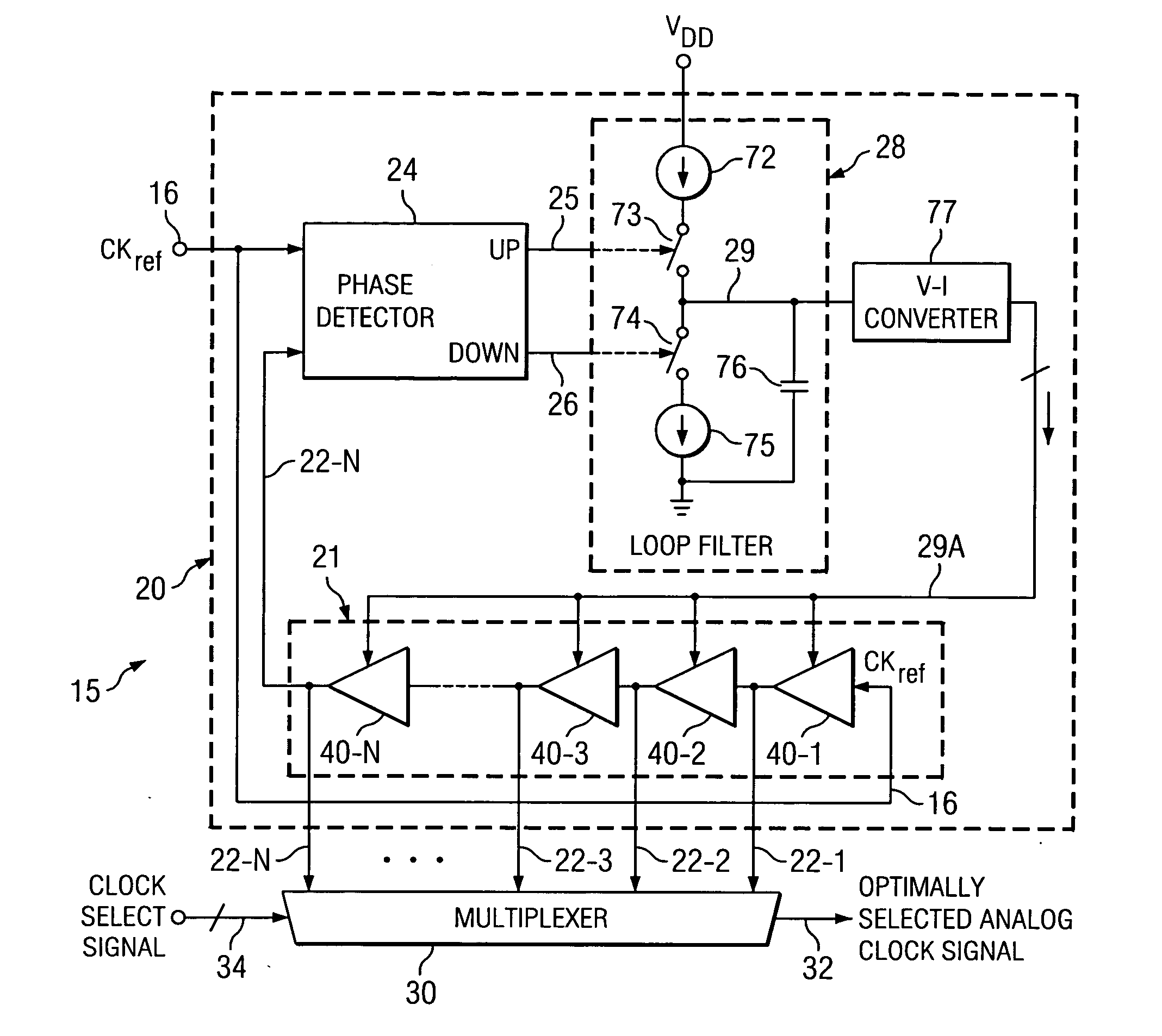
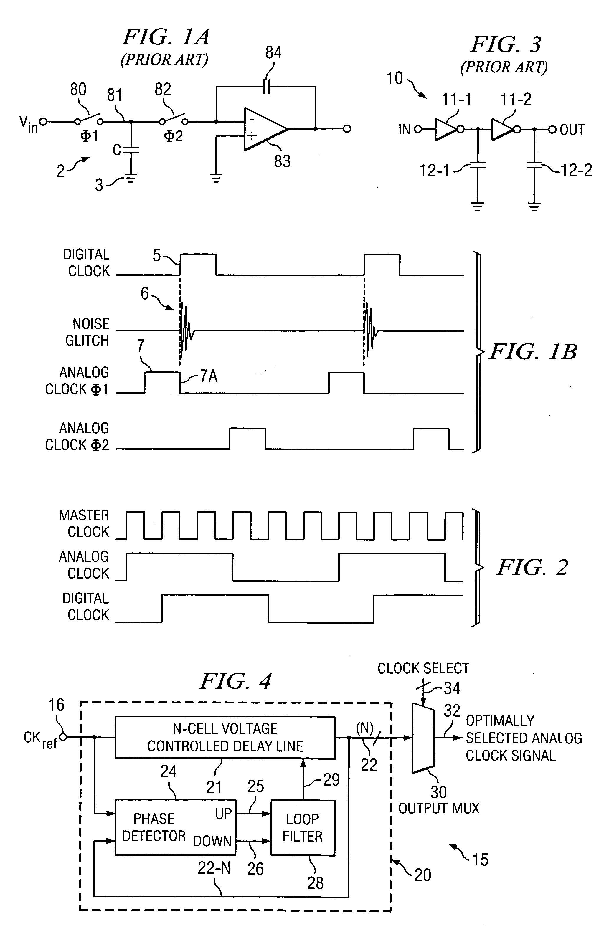
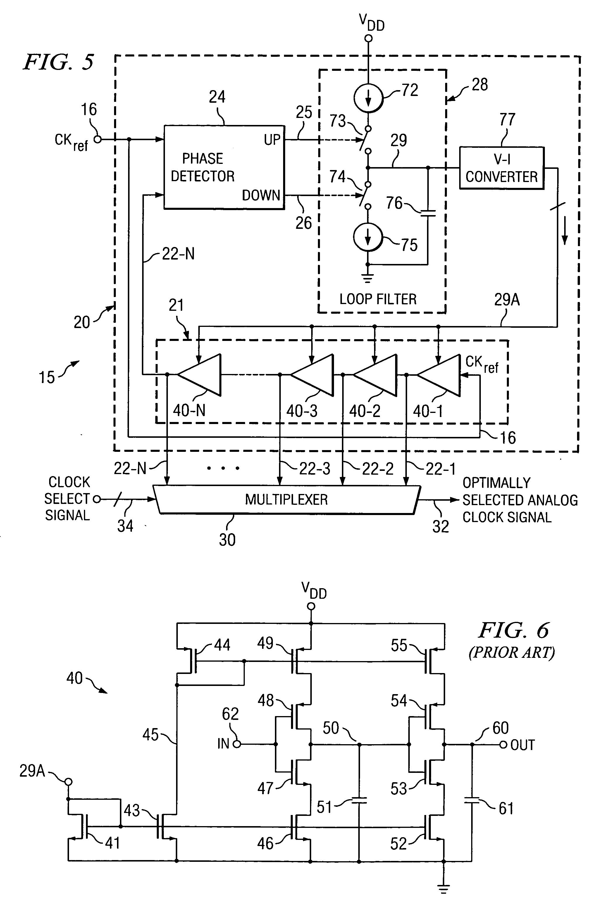
Delay locked loop circuitry and method for optimizing delay timing in mixed signal systems
PatentInactiveUS20060038596A1
Innovation
- A delay locked loop (DLL) circuit with a multiplexer is used to generate clock signals for both digital and analog circuits, allowing for optimal skewing of clock signals to minimize noise interference, independent of temperature and manufacturing process variations, without significant power consumption increases.

Apparatus for equalizing signal parameters in flip chip redistribution layers
PatentInactiveUS6025647A
Innovation
- A redistribution layer with patterned metallization that equalizes capacitance and resistance across traces by varying their widths and bump pad sizes, ensuring minimal skew and noise while maintaining high I/O density.
Thermal Management Considerations in RDL Design
Thermal management represents a critical design consideration in redistribution layer (RDL) optimization for mixed-signal systems, as heat generation and dissipation directly impact signal integrity, component reliability, and overall system performance. The increasing power densities in modern semiconductor packages, combined with the miniaturization trends in mixed-signal applications, have elevated thermal considerations from secondary concerns to primary design constraints that must be addressed during the initial RDL architecture planning phases.
The fundamental challenge lies in balancing electrical performance requirements with thermal constraints while maintaining manufacturing feasibility. RDL structures inherently create thermal bottlenecks due to their multi-layered metal interconnect architecture, where heat generated by active components must traverse through relatively thin dielectric layers with limited thermal conductivity. This thermal resistance becomes particularly problematic in mixed-signal systems where analog and digital circuits operate in close proximity, creating localized hot spots that can degrade sensitive analog performance through temperature-induced parameter variations.
Material selection plays a pivotal role in thermal management strategy, with traditional polyimide-based dielectrics offering limited thermal conductivity compared to emerging alternatives such as benzocyclobutene (BCB) or advanced epoxy formulations with thermal fillers. The trade-offs between dielectric constant, loss tangent, and thermal conductivity must be carefully evaluated, as materials with superior thermal properties may compromise electrical performance or introduce manufacturing complexities that offset their thermal benefits.
Geometric optimization of RDL structures provides additional thermal management opportunities through strategic placement of thermal vias, metal fill patterns, and heat spreading layers. The implementation of dedicated thermal pathways using high-conductivity metals such as copper or specialized thermal interface materials can significantly improve heat dissipation efficiency. However, these thermal enhancement features must be integrated without compromising the primary electrical routing requirements or introducing unwanted parasitic effects that could degrade signal quality.
Advanced thermal simulation and modeling techniques have become indispensable tools for RDL thermal optimization, enabling designers to predict temperature distributions, identify potential thermal issues, and evaluate mitigation strategies before physical prototyping. These computational approaches allow for comprehensive analysis of transient thermal behavior, which is particularly important in mixed-signal applications where power consumption patterns vary significantly between operational modes.
The integration of active thermal management solutions, such as micro-cooling structures or thermally adaptive materials, represents an emerging frontier in RDL thermal design, though practical implementation remains challenging due to space constraints and manufacturing complexity considerations.
The fundamental challenge lies in balancing electrical performance requirements with thermal constraints while maintaining manufacturing feasibility. RDL structures inherently create thermal bottlenecks due to their multi-layered metal interconnect architecture, where heat generated by active components must traverse through relatively thin dielectric layers with limited thermal conductivity. This thermal resistance becomes particularly problematic in mixed-signal systems where analog and digital circuits operate in close proximity, creating localized hot spots that can degrade sensitive analog performance through temperature-induced parameter variations.
Material selection plays a pivotal role in thermal management strategy, with traditional polyimide-based dielectrics offering limited thermal conductivity compared to emerging alternatives such as benzocyclobutene (BCB) or advanced epoxy formulations with thermal fillers. The trade-offs between dielectric constant, loss tangent, and thermal conductivity must be carefully evaluated, as materials with superior thermal properties may compromise electrical performance or introduce manufacturing complexities that offset their thermal benefits.
Geometric optimization of RDL structures provides additional thermal management opportunities through strategic placement of thermal vias, metal fill patterns, and heat spreading layers. The implementation of dedicated thermal pathways using high-conductivity metals such as copper or specialized thermal interface materials can significantly improve heat dissipation efficiency. However, these thermal enhancement features must be integrated without compromising the primary electrical routing requirements or introducing unwanted parasitic effects that could degrade signal quality.
Advanced thermal simulation and modeling techniques have become indispensable tools for RDL thermal optimization, enabling designers to predict temperature distributions, identify potential thermal issues, and evaluate mitigation strategies before physical prototyping. These computational approaches allow for comprehensive analysis of transient thermal behavior, which is particularly important in mixed-signal applications where power consumption patterns vary significantly between operational modes.
The integration of active thermal management solutions, such as micro-cooling structures or thermally adaptive materials, represents an emerging frontier in RDL thermal design, though practical implementation remains challenging due to space constraints and manufacturing complexity considerations.
Signal Integrity Standards for Mixed-Signal RDL Systems
Signal integrity standards for mixed-signal redistribution layer (RDL) systems represent a critical framework for ensuring reliable performance in advanced semiconductor packaging applications. These standards encompass comprehensive guidelines for electromagnetic compatibility, crosstalk mitigation, and signal quality preservation across heterogeneous signal domains within RDL architectures.
The IEEE 802.3 and JEDEC standards provide foundational specifications for high-speed digital signal transmission, while IPC-2221 and IPC-2226 establish design rules for mixed-signal PCB layouts that extend to RDL implementations. These standards define critical parameters including impedance control tolerances, via stub limitations, and differential pair matching requirements essential for maintaining signal fidelity in dense interconnect environments.
Power delivery network (PDN) integrity standards, particularly those outlined in IEEE 1597 series, address voltage regulation and noise suppression requirements specific to mixed-signal RDL systems. These specifications mandate maximum allowable power supply noise levels, typically limiting ripple to less than 5% of nominal voltage, while establishing guidelines for decoupling capacitor placement and power plane segmentation strategies.
Crosstalk mitigation standards focus on near-end and far-end crosstalk limitations, with JEDEC JESD204 specifying maximum coupling coefficients between adjacent signal traces. For mixed-signal applications, these standards require isolation barriers between analog and digital domains, mandating minimum spacing requirements and guard trace implementations to prevent interference between sensitive analog circuits and high-frequency digital switching networks.
Electromagnetic interference (EMI) compliance standards, including FCC Part 15 and CISPR 22, establish emission limits that directly impact RDL design methodologies. These regulations necessitate careful consideration of trace routing, via placement, and shielding techniques to minimize radiated emissions while maintaining optimal signal transmission characteristics.
Testing and validation standards, such as IPC-TM-650 and JEDEC JESD51 series, provide standardized methodologies for characterizing RDL performance parameters including insertion loss, return loss, and time-domain reflectometry measurements. These protocols ensure consistent evaluation criteria across different manufacturing processes and design implementations, enabling reliable performance prediction and quality assurance in production environments.
The IEEE 802.3 and JEDEC standards provide foundational specifications for high-speed digital signal transmission, while IPC-2221 and IPC-2226 establish design rules for mixed-signal PCB layouts that extend to RDL implementations. These standards define critical parameters including impedance control tolerances, via stub limitations, and differential pair matching requirements essential for maintaining signal fidelity in dense interconnect environments.
Power delivery network (PDN) integrity standards, particularly those outlined in IEEE 1597 series, address voltage regulation and noise suppression requirements specific to mixed-signal RDL systems. These specifications mandate maximum allowable power supply noise levels, typically limiting ripple to less than 5% of nominal voltage, while establishing guidelines for decoupling capacitor placement and power plane segmentation strategies.
Crosstalk mitigation standards focus on near-end and far-end crosstalk limitations, with JEDEC JESD204 specifying maximum coupling coefficients between adjacent signal traces. For mixed-signal applications, these standards require isolation barriers between analog and digital domains, mandating minimum spacing requirements and guard trace implementations to prevent interference between sensitive analog circuits and high-frequency digital switching networks.
Electromagnetic interference (EMI) compliance standards, including FCC Part 15 and CISPR 22, establish emission limits that directly impact RDL design methodologies. These regulations necessitate careful consideration of trace routing, via placement, and shielding techniques to minimize radiated emissions while maintaining optimal signal transmission characteristics.
Testing and validation standards, such as IPC-TM-650 and JEDEC JESD51 series, provide standardized methodologies for characterizing RDL performance parameters including insertion loss, return loss, and time-domain reflectometry measurements. These protocols ensure consistent evaluation criteria across different manufacturing processes and design implementations, enabling reliable performance prediction and quality assurance in production environments.
Unlock deeper insights with PatSnap Eureka Quick Research — get a full tech report to explore trends and direct your research. Try now!
Generate Your Research Report Instantly with AI Agent
Supercharge your innovation with PatSnap Eureka AI Agent Platform!