

Optimizing Semiconductor Burn-In to Prevent Early-Life Device Failures
MAY 25, 20269 MIN READ
Generate Your Research Report Instantly with AI Agent
PatSnap Eureka helps you evaluate technical feasibility & market potential.
Semiconductor Burn-In Technology Background and Objectives
Semiconductor burn-in technology emerged in the 1960s as a critical reliability assurance methodology within the semiconductor manufacturing industry. This technique was developed in response to the phenomenon known as the "bathtub curve" of device failure rates, where electronic components exhibit higher failure rates during their initial operational period before stabilizing to lower, steady-state failure rates. The technology involves subjecting semiconductor devices to elevated temperature and voltage stress conditions for predetermined durations to accelerate the manifestation of latent defects and weak components that would otherwise fail prematurely in field applications.
The historical evolution of burn-in technology has been closely intertwined with the advancement of semiconductor manufacturing processes and the increasing complexity of integrated circuits. Early implementations focused primarily on discrete components and simple integrated circuits, utilizing basic thermal stress chambers. As semiconductor technology progressed through various technology nodes, from micron-scale to nanometer-scale manufacturing, burn-in methodologies have evolved to address new failure mechanisms and reliability challenges associated with miniaturization, increased transistor density, and novel materials integration.
Contemporary burn-in technology encompasses multiple stress methodologies including static burn-in, dynamic burn-in, and high-temperature operating life testing. The technology has expanded beyond traditional thermal stress to incorporate voltage stress, current stress, and combined stress conditions tailored to specific device architectures and anticipated operating environments. Modern burn-in systems integrate sophisticated monitoring capabilities, real-time data acquisition, and adaptive stress profiling to optimize effectiveness while minimizing unnecessary stress exposure.
The primary objective of optimizing semiconductor burn-in processes centers on maximizing early-life failure detection while minimizing manufacturing costs and time-to-market impacts. This optimization seeks to establish optimal stress conditions, duration parameters, and screening criteria that effectively eliminate weak devices without compromising the reliability of robust components. The technology aims to achieve statistical confidence in shipped product reliability while maintaining economic viability in high-volume manufacturing environments.
Advanced burn-in optimization targets the development of predictive models and machine learning algorithms to enhance screening effectiveness and reduce over-testing. The objective includes establishing correlation models between burn-in stress conditions and field failure mechanisms, enabling more precise stress parameter selection and duration optimization. Furthermore, the technology evolution focuses on integrating burn-in processes with comprehensive quality management systems to enable continuous improvement and adaptive optimization based on field performance feedback and manufacturing process variations.
The historical evolution of burn-in technology has been closely intertwined with the advancement of semiconductor manufacturing processes and the increasing complexity of integrated circuits. Early implementations focused primarily on discrete components and simple integrated circuits, utilizing basic thermal stress chambers. As semiconductor technology progressed through various technology nodes, from micron-scale to nanometer-scale manufacturing, burn-in methodologies have evolved to address new failure mechanisms and reliability challenges associated with miniaturization, increased transistor density, and novel materials integration.
Contemporary burn-in technology encompasses multiple stress methodologies including static burn-in, dynamic burn-in, and high-temperature operating life testing. The technology has expanded beyond traditional thermal stress to incorporate voltage stress, current stress, and combined stress conditions tailored to specific device architectures and anticipated operating environments. Modern burn-in systems integrate sophisticated monitoring capabilities, real-time data acquisition, and adaptive stress profiling to optimize effectiveness while minimizing unnecessary stress exposure.
The primary objective of optimizing semiconductor burn-in processes centers on maximizing early-life failure detection while minimizing manufacturing costs and time-to-market impacts. This optimization seeks to establish optimal stress conditions, duration parameters, and screening criteria that effectively eliminate weak devices without compromising the reliability of robust components. The technology aims to achieve statistical confidence in shipped product reliability while maintaining economic viability in high-volume manufacturing environments.
Advanced burn-in optimization targets the development of predictive models and machine learning algorithms to enhance screening effectiveness and reduce over-testing. The objective includes establishing correlation models between burn-in stress conditions and field failure mechanisms, enabling more precise stress parameter selection and duration optimization. Furthermore, the technology evolution focuses on integrating burn-in processes with comprehensive quality management systems to enable continuous improvement and adaptive optimization based on field performance feedback and manufacturing process variations.
Market Demand for Reliable Semiconductor Devices
The global semiconductor industry faces unprecedented pressure to deliver highly reliable devices as electronic systems become increasingly critical across multiple sectors. Modern applications in automotive, aerospace, medical devices, and telecommunications demand semiconductor components that can operate flawlessly throughout their intended lifespan without unexpected failures that could compromise system integrity or safety.
Automotive electronics represent one of the most demanding markets for semiconductor reliability. Advanced driver assistance systems, electric vehicle power management, and autonomous driving technologies require semiconductors that can withstand harsh operating conditions while maintaining consistent performance. Early-life failures in these applications can result in catastrophic consequences, driving automotive manufacturers to impose stringent reliability requirements on their semiconductor suppliers.
The medical device industry similarly demands exceptional semiconductor reliability, particularly for implantable devices such as pacemakers, insulin pumps, and neural stimulators. These applications require semiconductors to function reliably for decades within the human body, where replacement or repair is complex and risky. Regulatory bodies enforce strict quality standards that necessitate comprehensive reliability testing and validation processes.
Data center and cloud computing infrastructure creates another significant demand driver for reliable semiconductors. Server processors, memory modules, and networking components must operate continuously with minimal downtime. Early-life failures in these environments can lead to service disruptions, data loss, and substantial financial losses for service providers and their customers.
The Internet of Things expansion has multiplied the number of deployed semiconductor devices exponentially, often in remote or inaccessible locations where maintenance is challenging or impossible. These applications require semiconductors with proven long-term reliability to minimize field failures and associated service costs.
Industrial automation and smart manufacturing systems increasingly rely on sophisticated semiconductor-based control systems that must operate reliably in harsh environments with temperature extremes, vibration, and electromagnetic interference. Unplanned downtime due to semiconductor failures can halt entire production lines, resulting in significant economic losses.
Consumer electronics manufacturers face intense competition and brand reputation risks associated with product recalls or warranty claims resulting from semiconductor failures. Market leaders increasingly prioritize supplier reliability track records when making sourcing decisions, creating competitive advantages for semiconductor manufacturers who can demonstrate superior reliability performance through optimized burn-in processes and comprehensive quality assurance programs.
Automotive electronics represent one of the most demanding markets for semiconductor reliability. Advanced driver assistance systems, electric vehicle power management, and autonomous driving technologies require semiconductors that can withstand harsh operating conditions while maintaining consistent performance. Early-life failures in these applications can result in catastrophic consequences, driving automotive manufacturers to impose stringent reliability requirements on their semiconductor suppliers.
The medical device industry similarly demands exceptional semiconductor reliability, particularly for implantable devices such as pacemakers, insulin pumps, and neural stimulators. These applications require semiconductors to function reliably for decades within the human body, where replacement or repair is complex and risky. Regulatory bodies enforce strict quality standards that necessitate comprehensive reliability testing and validation processes.
Data center and cloud computing infrastructure creates another significant demand driver for reliable semiconductors. Server processors, memory modules, and networking components must operate continuously with minimal downtime. Early-life failures in these environments can lead to service disruptions, data loss, and substantial financial losses for service providers and their customers.
The Internet of Things expansion has multiplied the number of deployed semiconductor devices exponentially, often in remote or inaccessible locations where maintenance is challenging or impossible. These applications require semiconductors with proven long-term reliability to minimize field failures and associated service costs.
Industrial automation and smart manufacturing systems increasingly rely on sophisticated semiconductor-based control systems that must operate reliably in harsh environments with temperature extremes, vibration, and electromagnetic interference. Unplanned downtime due to semiconductor failures can halt entire production lines, resulting in significant economic losses.
Consumer electronics manufacturers face intense competition and brand reputation risks associated with product recalls or warranty claims resulting from semiconductor failures. Market leaders increasingly prioritize supplier reliability track records when making sourcing decisions, creating competitive advantages for semiconductor manufacturers who can demonstrate superior reliability performance through optimized burn-in processes and comprehensive quality assurance programs.
Current Burn-In Challenges and Early Failure Issues
Semiconductor burn-in processes face significant challenges in effectively identifying and eliminating early-life failures while maintaining cost efficiency and production throughput. Traditional burn-in methods often rely on standardized temperature and voltage stress conditions that may not adequately replicate real-world operating environments, leading to incomplete screening of defective devices. This mismatch between test conditions and actual application scenarios results in latent defects escaping detection, subsequently manifesting as field failures within the first few months of operation.
Temperature uniformity across burn-in chambers presents another critical challenge, as thermal gradients can create inconsistent stress conditions among devices under test. Non-uniform heating leads to varying activation energies for failure mechanisms, causing some devices to experience insufficient stress while others may be over-stressed, potentially inducing new defects rather than revealing existing ones. Modern high-density packaging and advanced node technologies exacerbate this issue due to increased power densities and thermal management complexities.
Early failure mechanisms in contemporary semiconductors have evolved beyond traditional failure modes, with new challenges emerging from advanced manufacturing processes. Gate oxide integrity issues, electromigration in narrow interconnects, and stress-induced voiding in through-silicon vias represent failure modes that require specialized burn-in approaches. These mechanisms often exhibit complex dependencies on multiple stress factors, making single-parameter burn-in protocols insufficient for comprehensive screening.
Time-to-market pressures have intensified the conflict between thorough burn-in testing and production schedules. Extended burn-in durations necessary for effective screening of certain failure mechanisms conflict with aggressive product launch timelines, forcing manufacturers to make compromises that may impact long-term reliability. This challenge is particularly acute for consumer electronics where product lifecycles are short but reliability expectations remain high.
Cost optimization remains a persistent challenge as burn-in operations consume significant energy and require substantial capital investment in test equipment. The economic burden is amplified by the need for parallel testing of large device populations and the associated handling complexities. Additionally, determining optimal burn-in duration requires balancing the cost of extended testing against the potential costs of field failures and warranty claims.
Temperature uniformity across burn-in chambers presents another critical challenge, as thermal gradients can create inconsistent stress conditions among devices under test. Non-uniform heating leads to varying activation energies for failure mechanisms, causing some devices to experience insufficient stress while others may be over-stressed, potentially inducing new defects rather than revealing existing ones. Modern high-density packaging and advanced node technologies exacerbate this issue due to increased power densities and thermal management complexities.
Early failure mechanisms in contemporary semiconductors have evolved beyond traditional failure modes, with new challenges emerging from advanced manufacturing processes. Gate oxide integrity issues, electromigration in narrow interconnects, and stress-induced voiding in through-silicon vias represent failure modes that require specialized burn-in approaches. These mechanisms often exhibit complex dependencies on multiple stress factors, making single-parameter burn-in protocols insufficient for comprehensive screening.
Time-to-market pressures have intensified the conflict between thorough burn-in testing and production schedules. Extended burn-in durations necessary for effective screening of certain failure mechanisms conflict with aggressive product launch timelines, forcing manufacturers to make compromises that may impact long-term reliability. This challenge is particularly acute for consumer electronics where product lifecycles are short but reliability expectations remain high.
Cost optimization remains a persistent challenge as burn-in operations consume significant energy and require substantial capital investment in test equipment. The economic burden is amplified by the need for parallel testing of large device populations and the associated handling complexities. Additionally, determining optimal burn-in duration requires balancing the cost of extended testing against the potential costs of field failures and warranty claims.
Current Burn-In Optimization Solutions
01 Burn-in testing methodologies and apparatus
Various methodologies and apparatus are employed for conducting burn-in testing of semiconductor devices to identify early-life failures. These approaches include specialized test equipment, controlled environmental conditions, and systematic testing procedures that subject devices to accelerated stress conditions. The testing methodologies help manufacturers identify defective devices before they reach end users, improving overall product reliability and reducing field failures.- Burn-in testing methods and apparatus for semiconductor devices: Various methods and apparatus are employed for conducting burn-in testing on semiconductor devices to identify early-life failures. These approaches include specialized testing equipment, controlled environmental conditions, and systematic testing procedures that subject devices to accelerated stress conditions. The testing methods help manufacturers identify defective devices before they reach end users.
- Temperature and voltage stress testing for early failure detection: Semiconductor devices are subjected to elevated temperature and voltage stress conditions during burn-in processes to accelerate potential failure mechanisms. This approach helps identify devices that would fail prematurely under normal operating conditions. The stress testing parameters are carefully controlled to simulate extended operational periods in compressed timeframes.
- Automated burn-in systems and control mechanisms: Advanced automated systems are developed to manage and control burn-in processes for semiconductor devices. These systems incorporate sophisticated control mechanisms, monitoring capabilities, and data collection features to ensure consistent and reliable testing. The automation reduces human error and improves testing efficiency while maintaining precise control over testing parameters.
- Failure analysis and prediction methodologies: Comprehensive methodologies are employed to analyze failure patterns and predict early-life device failures in semiconductor components. These approaches involve statistical analysis, failure mode identification, and predictive modeling to understand failure mechanisms. The analysis helps improve manufacturing processes and develop more reliable screening methods.
- Specialized burn-in structures and device configurations: Specific structural designs and device configurations are developed to facilitate effective burn-in testing and early failure detection. These include specialized test structures, interconnection methods, and device layouts that enable efficient stress application and monitoring. The configurations are optimized to provide maximum stress coverage while maintaining device integrity during testing.
02 Temperature and voltage stress testing
Semiconductor devices are subjected to elevated temperature and voltage conditions during burn-in processes to accelerate potential failure mechanisms. This stress testing approach helps identify weak devices that might fail during normal operation by exposing them to conditions beyond typical operating parameters. The combination of thermal and electrical stress effectively screens out devices with latent defects or manufacturing irregularities.Expand Specific Solutions03 Failure analysis and detection systems
Advanced detection and analysis systems are implemented to monitor and identify device failures during burn-in testing. These systems employ various sensing techniques, data collection methods, and analytical algorithms to detect anomalous behavior or performance degradation. The failure detection capabilities enable real-time monitoring and classification of different failure modes, facilitating improved quality control processes.Expand Specific Solutions04 Automated burn-in control and monitoring
Automated control systems manage the burn-in process by regulating test conditions, monitoring device parameters, and controlling test duration. These systems provide precise control over environmental factors such as temperature, voltage, and timing while continuously monitoring device performance. Automation reduces human error, improves test consistency, and enables efficient processing of large quantities of semiconductor devices.Expand Specific Solutions05 Reliability prediction and lifetime estimation
Mathematical models and statistical methods are used to predict device reliability and estimate lifetime based on burn-in test results. These approaches analyze failure patterns, calculate failure rates, and extrapolate long-term reliability characteristics from accelerated test data. The predictive capabilities help manufacturers establish quality standards, optimize burn-in parameters, and provide reliability specifications for their semiconductor products.Expand Specific Solutions
Key Players in Semiconductor Testing Industry
The semiconductor burn-in optimization market represents a mature yet evolving segment within the broader semiconductor testing ecosystem, currently valued at several billion dollars globally. The industry is in a consolidation phase, with established players like Intel, Samsung Electronics, Micron Technology, and Texas Instruments dominating through their extensive manufacturing capabilities and R&D investments. Technology maturity varies significantly across the competitive landscape - while traditional semiconductor giants possess advanced burn-in methodologies integrated into their production lines, specialized testing companies like Advantest and FormFactor are pushing technological boundaries with innovative automated solutions. Emerging players such as SMIC and Renesas are rapidly advancing their capabilities, particularly in automotive and IoT applications where reliability is paramount. The market demonstrates a clear bifurcation between high-volume manufacturers implementing proprietary burn-in processes and specialized equipment providers developing next-generation testing platforms that leverage AI and machine learning for predictive failure analysis.
Intel Corp.
Technical Solution: Intel implements comprehensive burn-in optimization through advanced thermal cycling protocols and statistical process control. Their approach utilizes accelerated life testing with elevated temperature and voltage stress conditions, typically operating at 125°C for 24-168 hours depending on device complexity. Intel's burn-in methodology incorporates real-time monitoring systems that track device parameters during stress testing, enabling early detection of potential failure modes. The company employs machine learning algorithms to optimize burn-in duration and conditions based on historical failure data and device characteristics, reducing overall test time while maintaining reliability standards.
Strengths: Industry-leading statistical analysis capabilities and extensive historical data for optimization. Weaknesses: High energy consumption and longer test cycles compared to some competitors.
Advantest Corp.
Technical Solution: Advantest provides comprehensive burn-in test solutions through their advanced automated test equipment and optimization software. Their approach integrates burn-in chambers with sophisticated measurement capabilities, enabling real-time monitoring of device parameters during stress testing. Advantest's methodology employs statistical process control and data analytics to optimize burn-in conditions, including temperature ramping profiles, voltage stress levels, and test duration. The company offers adaptive burn-in algorithms that adjust test parameters based on device response and failure rate targets. Their solutions include predictive maintenance capabilities and automated data analysis tools that help semiconductor manufacturers reduce burn-in costs while improving reliability screening effectiveness.
Strengths: Comprehensive test equipment integration and advanced automation capabilities. Weaknesses: Dependency on external equipment suppliers and higher initial investment costs.
Core Patents in Advanced Burn-In Technologies
Method and apparatus to achieve more level thermal gradient
PatentActiveUS20080147976A1
Innovation
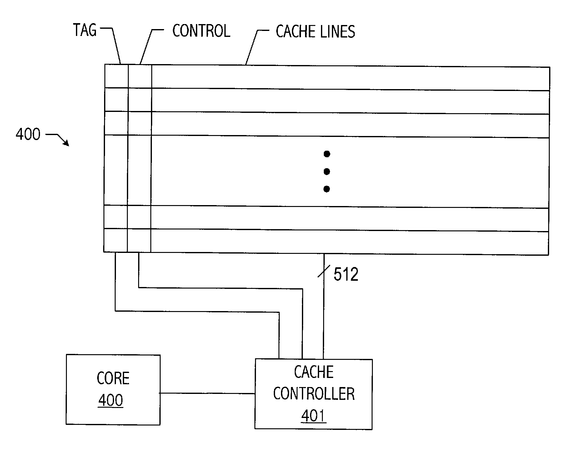
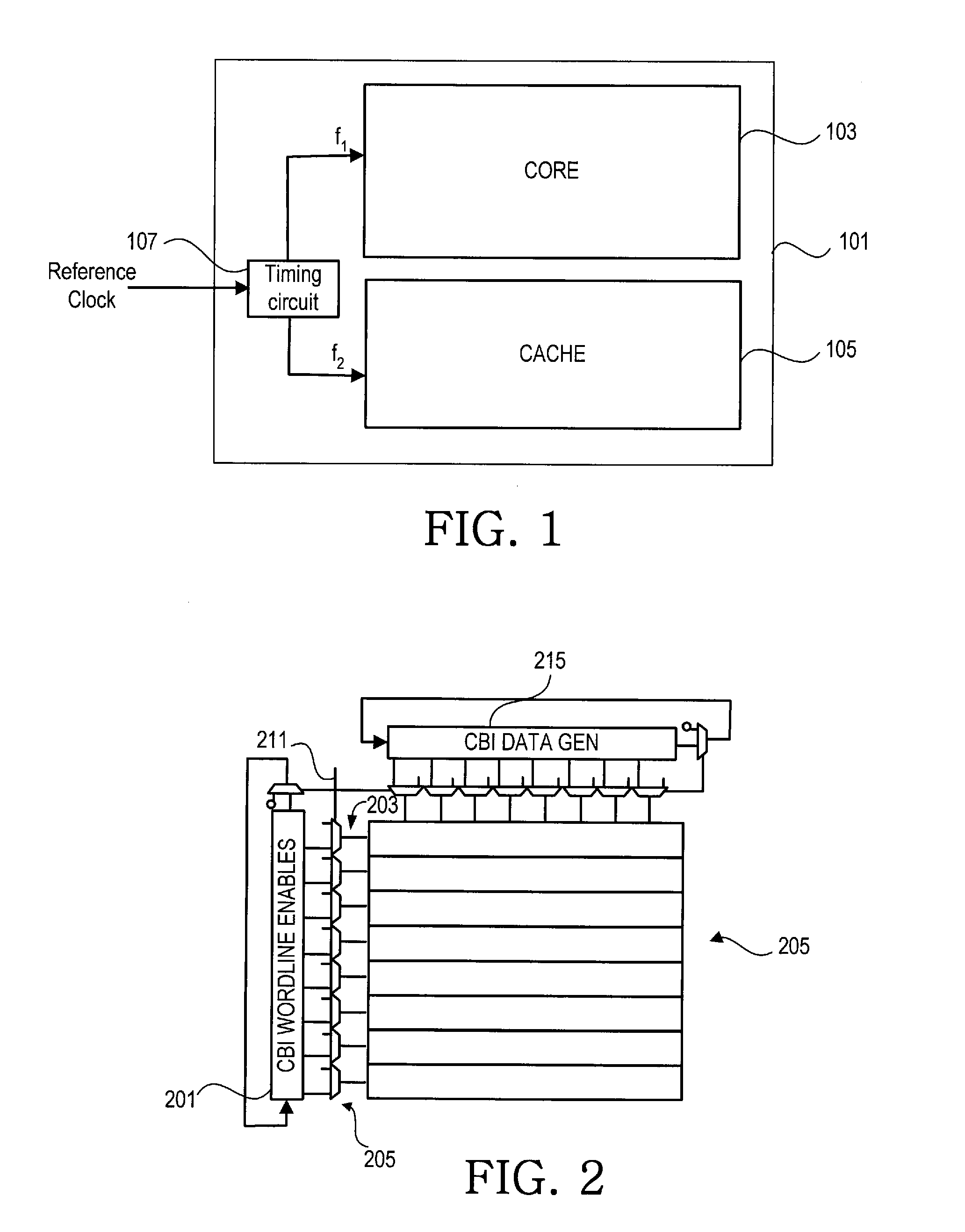
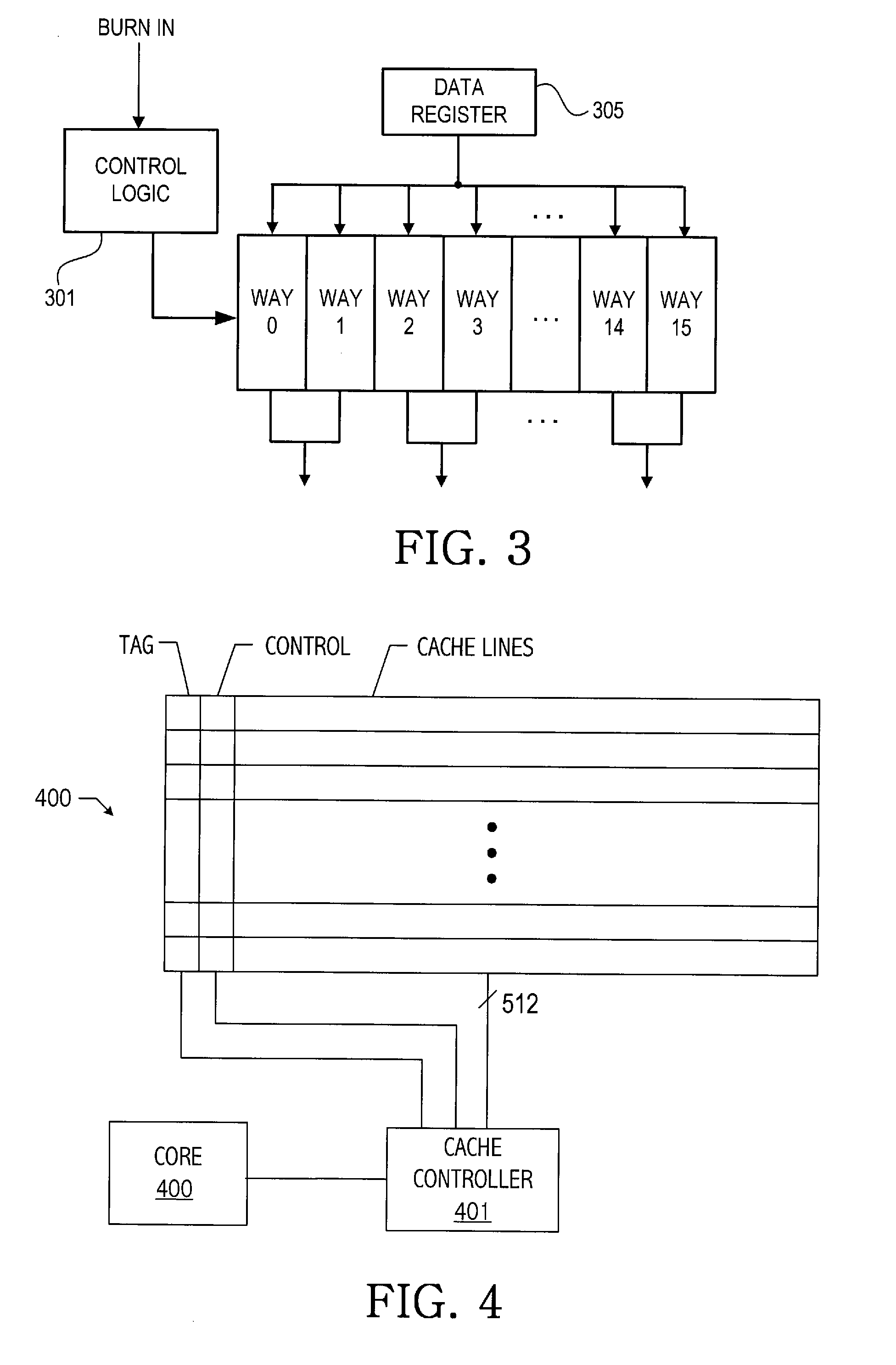
- Increasing cache activity during burn-in by simultaneously accessing multiple memory locations and operating the cache at higher frequencies, while reducing core frequency to achieve more uniform power density and reduce thermal gradients, thereby ensuring all areas of the die are subjected to consistent temperature acceleration.

Methodology for reducing post burn-in VMIN drift
PatentWO2009023694A2
Innovation
- Implementing a nitrogen-doped polysilicon electrode with a higher nitrogen concentration than the source/drain regions, where nitrogen is implanted into the gate electrode layer before forming the gate electrode to reduce grain boundary defects and stabilize Vmin, thereby minimizing impurity regions and gate leakage.


Quality Standards for Semiconductor Reliability Testing
Quality standards for semiconductor reliability testing form the backbone of effective burn-in optimization strategies, establishing critical benchmarks that ensure device longevity and performance consistency. These standards encompass multiple testing protocols designed to validate semiconductor components under various stress conditions, providing manufacturers with quantifiable metrics to assess device reliability before market deployment.
The Joint Electron Device Engineering Council (JEDEC) standards serve as the primary framework for semiconductor reliability testing, with JESD22 series specifically addressing environmental and mechanical stress testing procedures. These standards define precise temperature cycling parameters, humidity exposure limits, and mechanical shock thresholds that devices must withstand during qualification testing. JEDEC 22-A108 establishes temperature cycling test conditions, while JEDEC 22-A101 specifies steady-state temperature humidity bias testing protocols essential for burn-in validation.
International Electrotechnical Commission (IEC) standards complement JEDEC specifications by providing broader reliability assessment frameworks. IEC 60749 series outlines comprehensive semiconductor device mechanical and climatic test methods, establishing statistical sampling procedures and failure criteria that directly influence burn-in test design. These standards mandate specific test durations, sample sizes, and acceptance criteria that manufacturers must incorporate into their burn-in optimization strategies.
Military and aerospace applications require adherence to MIL-STD-883 standards, which impose more stringent reliability requirements than commercial specifications. These standards define extended burn-in durations, elevated stress conditions, and enhanced screening procedures necessary for high-reliability applications. The standard's Method 1015 specifically addresses steady-state life testing protocols that inform optimal burn-in parameter selection for critical applications.
Automotive semiconductor reliability follows AEC-Q qualification standards, which establish specific stress testing requirements for automotive electronic components. AEC-Q100 for integrated circuits and AEC-Q101 for discrete semiconductors define temperature cycling, high-temperature operating life, and power cycling test conditions that directly correlate with effective burn-in strategies. These standards emphasize early failure detection through accelerated stress testing methodologies.
Statistical process control standards, including ISO 16949 and Six Sigma methodologies, provide quality frameworks for implementing and monitoring burn-in processes. These standards establish control chart procedures, capability indices, and continuous improvement protocols that ensure burn-in optimization efforts maintain statistical validity and process consistency across manufacturing operations.
The Joint Electron Device Engineering Council (JEDEC) standards serve as the primary framework for semiconductor reliability testing, with JESD22 series specifically addressing environmental and mechanical stress testing procedures. These standards define precise temperature cycling parameters, humidity exposure limits, and mechanical shock thresholds that devices must withstand during qualification testing. JEDEC 22-A108 establishes temperature cycling test conditions, while JEDEC 22-A101 specifies steady-state temperature humidity bias testing protocols essential for burn-in validation.
International Electrotechnical Commission (IEC) standards complement JEDEC specifications by providing broader reliability assessment frameworks. IEC 60749 series outlines comprehensive semiconductor device mechanical and climatic test methods, establishing statistical sampling procedures and failure criteria that directly influence burn-in test design. These standards mandate specific test durations, sample sizes, and acceptance criteria that manufacturers must incorporate into their burn-in optimization strategies.
Military and aerospace applications require adherence to MIL-STD-883 standards, which impose more stringent reliability requirements than commercial specifications. These standards define extended burn-in durations, elevated stress conditions, and enhanced screening procedures necessary for high-reliability applications. The standard's Method 1015 specifically addresses steady-state life testing protocols that inform optimal burn-in parameter selection for critical applications.
Automotive semiconductor reliability follows AEC-Q qualification standards, which establish specific stress testing requirements for automotive electronic components. AEC-Q100 for integrated circuits and AEC-Q101 for discrete semiconductors define temperature cycling, high-temperature operating life, and power cycling test conditions that directly correlate with effective burn-in strategies. These standards emphasize early failure detection through accelerated stress testing methodologies.
Statistical process control standards, including ISO 16949 and Six Sigma methodologies, provide quality frameworks for implementing and monitoring burn-in processes. These standards establish control chart procedures, capability indices, and continuous improvement protocols that ensure burn-in optimization efforts maintain statistical validity and process consistency across manufacturing operations.
Cost-Effectiveness Analysis of Burn-In Processes
The cost-effectiveness analysis of semiconductor burn-in processes requires a comprehensive evaluation of the financial trade-offs between upfront testing investments and long-term reliability benefits. Traditional burn-in operations typically consume 15-25% of total manufacturing costs, making economic optimization crucial for maintaining competitive positioning while ensuring device reliability standards.
Direct cost components include burn-in equipment acquisition, facility infrastructure, energy consumption, and labor resources. High-temperature burn-in chambers represent significant capital expenditures, with advanced systems costing $500,000 to $2 million per unit. Energy costs constitute approximately 40-60% of operational expenses, as burn-in processes require sustained elevated temperatures and continuous monitoring for 24-168 hours depending on device specifications.
The economic benefits manifest through reduced warranty claims, enhanced customer satisfaction, and preserved brand reputation. Statistical analysis indicates that effective burn-in implementation can reduce field failure rates by 70-90% during the first year of operation. For high-volume consumer electronics, this translates to warranty cost savings of $0.50-$2.00 per device, often exceeding burn-in processing costs of $0.30-$1.20 per unit.
Return on investment calculations demonstrate varying outcomes across different semiconductor categories. Memory devices and microprocessors typically achieve positive ROI within 12-18 months due to high failure costs and volume economics. Conversely, low-cost commodity chips may require alternative screening approaches to maintain profitability margins.
Advanced burn-in optimization strategies focus on adaptive testing protocols that adjust duration and stress levels based on real-time failure data. Machine learning algorithms can reduce burn-in time by 30-50% while maintaining equivalent screening effectiveness, significantly improving cost efficiency. Predictive models enable targeted burn-in application, concentrating resources on high-risk device populations rather than universal processing.
The emergence of alternative reliability screening methods, including statistical sampling and accelerated life testing, provides cost-effective alternatives for specific applications. These approaches can reduce screening costs by 40-70% while maintaining acceptable reliability levels for non-critical applications, enabling manufacturers to optimize resource allocation across diverse product portfolios.
Direct cost components include burn-in equipment acquisition, facility infrastructure, energy consumption, and labor resources. High-temperature burn-in chambers represent significant capital expenditures, with advanced systems costing $500,000 to $2 million per unit. Energy costs constitute approximately 40-60% of operational expenses, as burn-in processes require sustained elevated temperatures and continuous monitoring for 24-168 hours depending on device specifications.
The economic benefits manifest through reduced warranty claims, enhanced customer satisfaction, and preserved brand reputation. Statistical analysis indicates that effective burn-in implementation can reduce field failure rates by 70-90% during the first year of operation. For high-volume consumer electronics, this translates to warranty cost savings of $0.50-$2.00 per device, often exceeding burn-in processing costs of $0.30-$1.20 per unit.
Return on investment calculations demonstrate varying outcomes across different semiconductor categories. Memory devices and microprocessors typically achieve positive ROI within 12-18 months due to high failure costs and volume economics. Conversely, low-cost commodity chips may require alternative screening approaches to maintain profitability margins.
Advanced burn-in optimization strategies focus on adaptive testing protocols that adjust duration and stress levels based on real-time failure data. Machine learning algorithms can reduce burn-in time by 30-50% while maintaining equivalent screening effectiveness, significantly improving cost efficiency. Predictive models enable targeted burn-in application, concentrating resources on high-risk device populations rather than universal processing.
The emergence of alternative reliability screening methods, including statistical sampling and accelerated life testing, provides cost-effective alternatives for specific applications. These approaches can reduce screening costs by 40-70% while maintaining acceptable reliability levels for non-critical applications, enabling manufacturers to optimize resource allocation across diverse product portfolios.
Unlock deeper insights with PatSnap Eureka Quick Research — get a full tech report to explore trends and direct your research. Try now!
Generate Your Research Report Instantly with AI Agent
Supercharge your innovation with PatSnap Eureka AI Agent Platform!