

Optimizing Space Utilization in 3D DRAM Layouts
APR 15, 20269 MIN READ
Generate Your Research Report Instantly with AI Agent
PatSnap Eureka helps you evaluate technical feasibility & market potential.
3D DRAM Space Optimization Background and Objectives
The evolution of memory technology has been fundamentally driven by the relentless pursuit of higher density, improved performance, and reduced cost per bit. Traditional planar DRAM architectures have reached critical scaling limitations as semiconductor manufacturing approaches physical boundaries at advanced process nodes. The transition from two-dimensional to three-dimensional memory structures represents a paradigm shift that addresses these fundamental constraints while opening new avenues for memory system optimization.
Three-dimensional DRAM technology emerged as a revolutionary approach to overcome the spatial limitations inherent in conventional memory designs. By stacking memory cells vertically, 3D DRAM architectures enable significant density improvements without proportional increases in chip footprint. This vertical integration approach has transformed the memory landscape, allowing manufacturers to achieve higher capacities while maintaining or improving performance characteristics.
The historical development of 3D DRAM can be traced through several key technological milestones. Early implementations focused on simple stacking techniques, gradually evolving toward sophisticated through-silicon via (TSV) technologies and advanced interconnect solutions. Each generation has brought improvements in layer count, interconnect density, and thermal management capabilities, establishing the foundation for current space optimization challenges.
Contemporary 3D DRAM layouts face increasingly complex spatial constraints as layer counts continue to increase. The challenge extends beyond simple vertical stacking to encompass comprehensive three-dimensional space utilization optimization. Critical factors include minimizing dead space between functional elements, optimizing interconnect routing efficiency, and maintaining thermal dissipation pathways while maximizing memory cell density.
The primary objective of 3D DRAM space optimization centers on achieving maximum storage density per unit volume while preserving electrical performance and reliability characteristics. This involves developing sophisticated layout algorithms that can efficiently pack memory cells, peripheral circuits, and interconnect structures within the three-dimensional design space. Secondary objectives include minimizing manufacturing complexity, reducing power consumption, and ensuring scalability for future technology nodes.
Advanced space optimization techniques must address multiple competing requirements simultaneously. These include maintaining adequate spacing for manufacturing tolerances, ensuring proper electrical isolation between layers, providing sufficient thermal management capabilities, and enabling efficient data access patterns. The optimization process requires balancing these diverse constraints while maximizing the effective utilization of available silicon real estate.
Market Demand for High-Density Memory Solutions
The global memory market is experiencing unprecedented demand driven by the exponential growth of data-intensive applications across multiple sectors. Cloud computing infrastructure, artificial intelligence workloads, and high-performance computing systems require increasingly sophisticated memory solutions that can deliver both capacity and performance within constrained physical footprints. This convergence of requirements has created a critical market need for high-density memory architectures that maximize storage capacity per unit volume.
Enterprise data centers represent the largest segment driving demand for high-density memory solutions. As organizations migrate to cloud-first strategies and implement AI-driven analytics, server architectures must accommodate larger memory pools while maintaining energy efficiency and thermal management. The proliferation of in-memory databases and real-time analytics platforms has intensified requirements for memory systems that can support both high bandwidth and substantial capacity within standard server form factors.
Mobile computing and edge devices constitute another significant market driver for space-optimized memory solutions. Smartphones, tablets, and IoT devices demand memory architectures that deliver desktop-class performance while fitting within increasingly compact device profiles. The integration of advanced camera systems, augmented reality capabilities, and on-device AI processing has created substantial pressure for memory solutions that maximize density without compromising power efficiency or thermal characteristics.
Automotive applications are emerging as a rapidly growing market segment for high-density memory solutions. Advanced driver assistance systems, autonomous vehicle platforms, and in-vehicle infotainment systems require memory architectures capable of processing vast amounts of sensor data in real-time. The automotive industry's transition toward software-defined vehicles has created demand for memory solutions that can support complex computational workloads within the space and weight constraints of automotive electronics.
The gaming and graphics processing market continues to drive innovation in high-density memory architectures. Modern graphics cards and gaming consoles require memory systems that can support increasingly complex visual rendering while maintaining compact form factors. The emergence of ray tracing, 4K gaming, and virtual reality applications has intensified demand for memory solutions that maximize bandwidth and capacity within thermal and spatial limitations.
Industrial and scientific computing applications represent specialized but significant market segments for advanced memory architectures. High-performance computing clusters, scientific simulation systems, and industrial automation platforms require memory solutions that can support massive datasets while operating reliably in demanding environmental conditions. These applications often prioritize memory density and reliability over cost considerations, creating opportunities for premium high-density memory solutions.
Current 3D DRAM Layout Challenges and Constraints
The current landscape of 3D DRAM technology faces significant architectural constraints that fundamentally limit space utilization efficiency. Traditional planar DRAM designs, when extended into three-dimensional structures, encounter exponential complexity in routing and interconnection management. The vertical stacking approach requires sophisticated through-silicon via (TSV) technologies, which consume substantial silicon real estate and introduce parasitic capacitances that degrade signal integrity.
Thermal management represents one of the most critical challenges in contemporary 3D DRAM implementations. Heat dissipation becomes increasingly problematic as memory layers are stacked vertically, creating thermal hotspots that can exceed operational temperature thresholds. The inner layers experience reduced heat dissipation capabilities, leading to performance throttling and reliability concerns. Current thermal solutions often require additional spacing between layers, directly compromising space utilization objectives.
Manufacturing precision limitations impose strict constraints on achievable layer densities and interconnect geometries. Current lithographic processes struggle to maintain consistent feature sizes across multiple stacked layers, particularly for critical dimensions below 10 nanometers. Process variations become amplified in vertical structures, resulting in yield degradation and necessitating conservative design margins that reduce overall space efficiency.
Power delivery networks in 3D DRAM architectures face unprecedented complexity challenges. Distributing stable power across multiple vertical layers while minimizing voltage drops requires extensive power grid infrastructure. The increased resistance and inductance of vertical power delivery paths demand wider conductors and additional decoupling capacitors, consuming valuable silicon area that could otherwise accommodate memory cells.
Signal integrity degradation emerges as a fundamental constraint in dense 3D layouts. Crosstalk between adjacent layers and within densely packed interconnects creates noise margins that limit operational frequencies. The electromagnetic coupling effects in three-dimensional structures require sophisticated shielding techniques and increased spacing between signal paths, directly impacting achievable memory density.
Access time penalties represent another significant constraint in current 3D DRAM designs. The hierarchical nature of vertical memory access introduces additional latency layers, particularly for cells located in upper tiers. Current addressing schemes often require sequential layer activation, creating bottlenecks that limit the practical benefits of increased storage density.
Existing 3D DRAM Space Utilization Solutions
01 Vertical stacking of memory cells in 3D DRAM architecture
Three-dimensional DRAM structures utilize vertical stacking techniques to arrange memory cells in multiple layers above the substrate. This approach significantly increases memory density by exploiting the vertical dimension rather than relying solely on planar scaling. The vertical integration allows for more memory capacity within the same footprint, improving space utilization through multi-layer cell arrangements and interconnect structures that enable efficient data access across stacked layers.- Vertical stacking of memory cells in 3D DRAM architecture: Three-dimensional DRAM structures utilize vertical stacking techniques to arrange memory cells in multiple layers above the substrate. This approach significantly increases memory density by exploiting the vertical dimension rather than relying solely on planar scaling. The vertical integration allows for more memory capacity within the same footprint, improving space utilization through multi-layer cell arrangements and interconnect structures that enable efficient data access across stacked layers.
- Through-silicon via (TSV) technology for inter-layer connections: Through-silicon vias provide vertical electrical connections between stacked memory layers in three-dimensional DRAM configurations. This technology enables efficient signal transmission and power delivery across multiple die layers while minimizing the horizontal space required for interconnections. The implementation of TSV structures allows for compact integration of memory arrays and reduces the overall footprint by eliminating the need for extensive lateral routing, thereby maximizing the effective use of available silicon area.
- Optimized cell layout and array organization: Advanced layout techniques focus on maximizing the packing density of memory cells through innovative array organizations and cell arrangements. These approaches include optimized bit line and word line configurations, reduced cell pitch dimensions, and efficient peripheral circuit placement. The layout strategies aim to minimize dead space between functional elements while maintaining signal integrity and manufacturability, resulting in higher memory capacity per unit area.
- Hybrid memory architectures combining DRAM with logic circuits: Integrated designs that combine three-dimensional DRAM structures with logic processing elements on the same chip or in closely stacked configurations. This integration approach reduces the physical distance between memory and processing units, improving data transfer efficiency while optimizing overall space utilization. The hybrid architecture allows for better resource allocation by positioning computational elements in proximity to memory arrays, reducing the need for extensive interconnect infrastructure.
- Advanced packaging techniques for 3D memory integration: Sophisticated packaging methods enable the integration of multiple memory dies in three-dimensional configurations with minimal spacing between layers. These techniques include wafer-to-wafer bonding, die-to-wafer bonding, and advanced encapsulation methods that allow for tight vertical integration. The packaging approaches focus on reducing the overall package height while maximizing memory density, incorporating thermal management solutions and ensuring reliable electrical connections between stacked components to achieve optimal space efficiency.
02 Through-silicon via (TSV) technology for inter-layer connections
Through-silicon vias provide vertical electrical connections between stacked memory layers in three-dimensional DRAM configurations. This technology enables efficient signal transmission and power delivery across multiple die layers while minimizing the horizontal space required for interconnections. The implementation of TSV structures allows for compact integration of memory arrays and reduces the overall package size, thereby maximizing the effective use of available silicon area.Expand Specific Solutions03 Optimized cell layout and array organization
Advanced layout techniques focus on optimizing the arrangement of memory cells, bit lines, and word lines to maximize storage density in three-dimensional configurations. These designs incorporate innovative cell geometries and array organizations that reduce the pitch between adjacent cells while maintaining reliable operation. The optimization strategies include folded bit-line architectures, shared peripheral circuits, and efficient routing schemes that minimize dead space and improve overall area efficiency.Expand Specific Solutions04 Hybrid memory cube and stacked die packaging
Hybrid memory cube architectures combine multiple DRAM dies in a vertically stacked configuration with high-bandwidth interconnects. This packaging approach integrates logic and memory layers to create compact, high-performance memory systems. The stacked die methodology reduces the footprint required for memory subsystems while providing increased bandwidth and reduced latency through shorter interconnect paths between processing and storage elements.Expand Specific Solutions05 Capacitor structure optimization for 3D integration
Three-dimensional DRAM designs employ specialized capacitor structures that are optimized for vertical integration while maintaining sufficient charge storage capacity. These structures utilize innovative geometries such as cylindrical, pillar, or trench configurations that extend vertically to maximize capacitance within limited lateral dimensions. The optimized capacitor designs enable higher cell density by reducing the area occupied by each storage element while ensuring adequate refresh characteristics and data retention.Expand Specific Solutions
Key Players in 3D DRAM and Memory Industry
The 3D DRAM layout optimization field represents a rapidly evolving segment within the memory semiconductor industry, currently in its growth phase as manufacturers seek to overcome traditional scaling limitations. The market demonstrates substantial potential, driven by increasing demand for high-density memory solutions in data centers, mobile devices, and AI applications. Technology maturity varies significantly across key players, with established memory giants like Samsung Electronics, Micron Technology, and ChangXin Memory Technologies leading commercial 3D DRAM development through advanced stacking architectures. Chinese companies including Yangtze Memory Technologies and research institutions like the Institute of Microelectronics demonstrate strong R&D capabilities, while equipment providers such as Applied Materials enable critical manufacturing processes. The competitive landscape shows a mix of mature commercial solutions and emerging innovations, with companies like Neo Semiconductor exploring novel approaches to three-dimensional memory architectures, indicating the technology is transitioning from experimental phases toward mainstream adoption.
Yangtze Memory Technologies Co., Ltd.
Technical Solution: Yangtze Memory has developed innovative 3D DRAM architectures focusing on vertical cell stacking with optimized space utilization through their proprietary Xtacking technology. Their approach integrates memory cells and peripheral circuits in separate layers, enabling independent optimization of each component for maximum density. The company implements advanced layout algorithms that consider thermal distribution and electrical interference to achieve optimal cell placement. Their 3D DRAM designs feature novel interconnect structures that reduce the overall footprint while maintaining high-speed data access. Yangtze Memory's solutions incorporate intelligent space management techniques that can achieve up to 50% better area efficiency compared to conventional 2D layouts through optimized vertical integration and minimized dead space.
Strengths: Innovative Xtacking technology provides unique advantages in 3D integration and space optimization. Weaknesses: Relatively newer market presence may limit established partnerships and ecosystem support.
Huawei Technologies Co., Ltd.
Technical Solution: Huawei's 3D DRAM space optimization focuses on AI-driven layout design and system-level integration for mobile and edge computing applications. Their approach utilizes machine learning algorithms to optimize cell placement and routing in 3D structures, considering power consumption, thermal characteristics, and performance requirements simultaneously. The company develops adaptive memory architectures that can dynamically reconfigure layout parameters based on workload patterns to maximize space efficiency. Huawei's solutions incorporate advanced compression techniques and intelligent data management to reduce physical storage requirements while maintaining high performance. Their 3D DRAM designs feature novel interconnect topologies and optimized peripheral circuit placement that can achieve significant space savings in compact device form factors.
Strengths: Strong AI and system integration capabilities enable intelligent optimization approaches. Weaknesses: Geopolitical restrictions may limit access to advanced manufacturing technologies and international collaborations.
Core Innovations in 3D Memory Layout Optimization
Dynamic random access memory array, semiconductor layout structure and fabrication method thereof
PatentActiveUS20200279594A1
Innovation
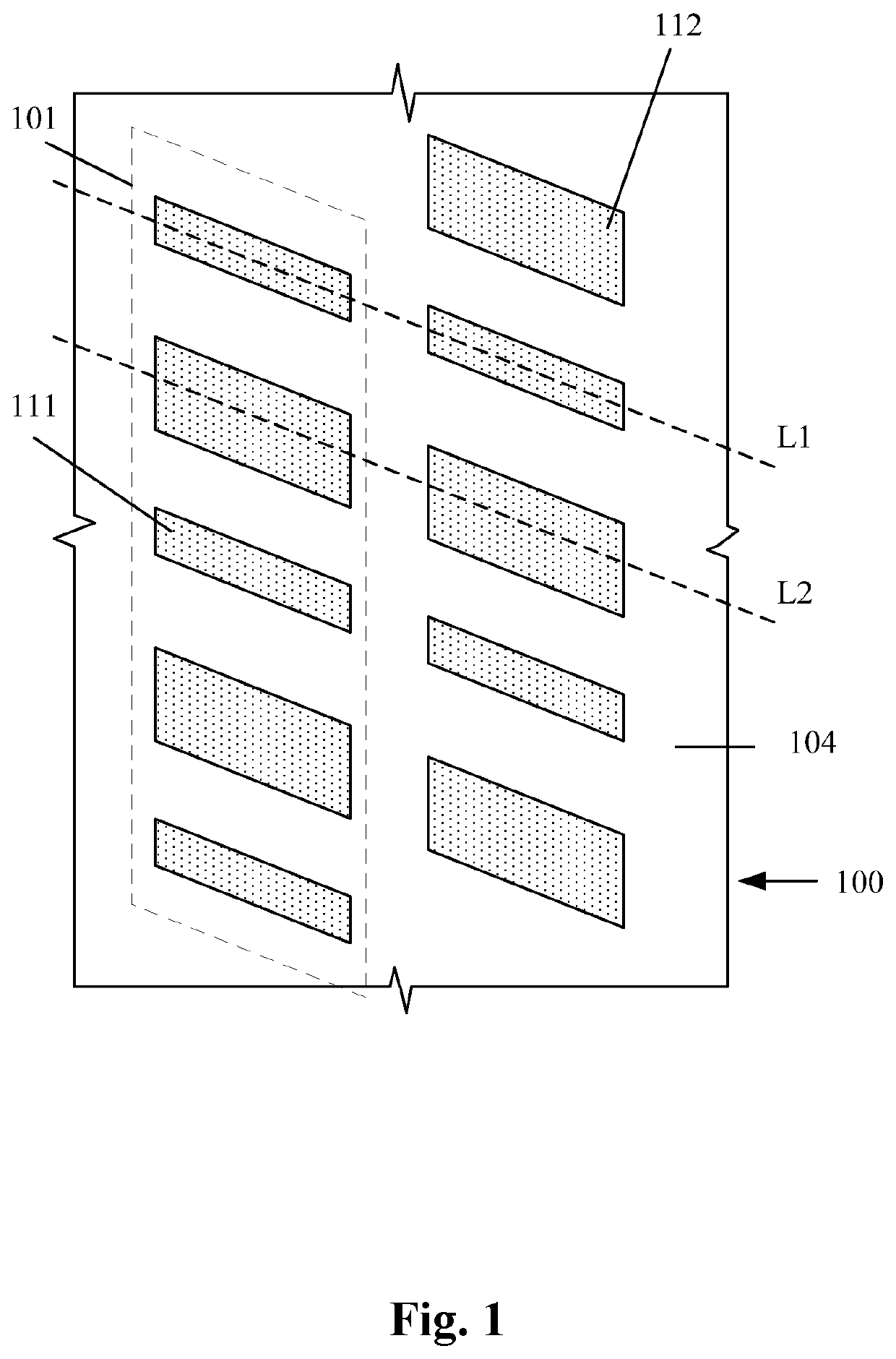
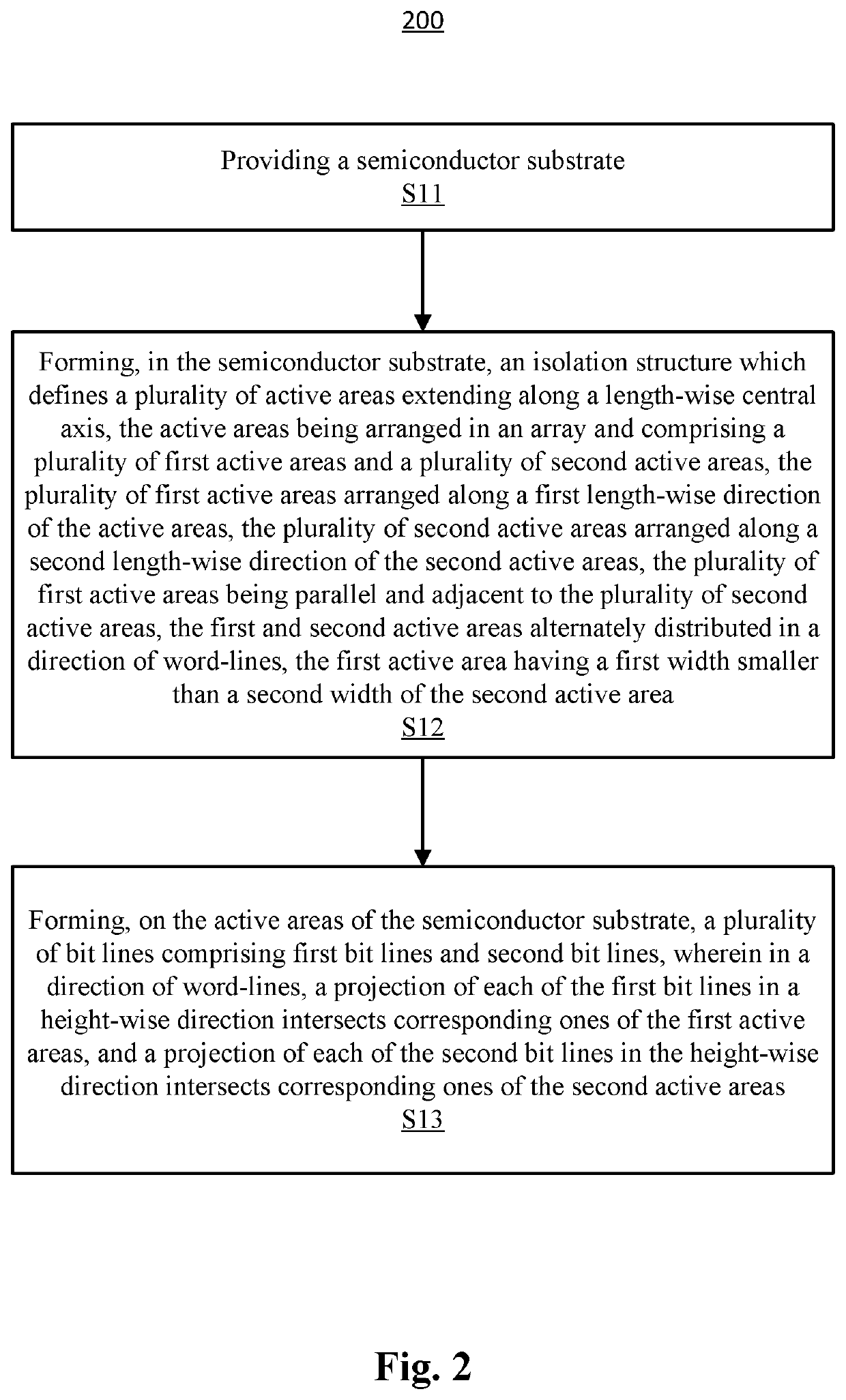
- A semiconductor layout structure for a DRAM array is designed with alternating active areas of different widths, where first active areas have a smaller width than second active areas, and bit lines intersect these areas, facilitating the formation of capacitors with different charge storage capacities, thereby improving device performance.

Three-dimensional memory array and preparation method thereof, memory and electronic equipment
PatentPendingCN118742020A
Innovation
- A three-dimensional storage array design is adopted, in which two storage units corresponding to the through-columns are set up in each storage layer. The peripheral area of the through-columns is rationally arranged to increase the density of the memory cells. The semi-ring structure is used to reduce the size of the memory cells and improve the storage density. .


Thermal Management in High-Density 3D Memory
Thermal management represents one of the most critical challenges in high-density 3D memory architectures, where the vertical stacking of multiple DRAM layers creates unprecedented heat generation and dissipation complexities. As memory cells are densely packed in three-dimensional configurations, the thermal density can reach levels that significantly impact both performance and reliability, making effective thermal control essential for practical implementation.
The fundamental challenge stems from the inherent heat generation characteristics of DRAM operations, where each memory access, refresh cycle, and standby operation contributes to thermal buildup. In traditional 2D layouts, heat dissipation occurs primarily through the substrate and packaging interfaces. However, 3D architectures introduce thermal resistance between stacked layers, creating hotspots in intermediate layers that are thermally isolated from primary heat dissipation paths.
Temperature gradients across different layers pose significant operational challenges, as elevated temperatures accelerate charge leakage in DRAM cells, reducing data retention times and increasing refresh frequency requirements. This thermal-induced performance degradation creates a cascading effect where increased refresh operations generate additional heat, potentially leading to thermal runaway scenarios in poorly managed systems.
Advanced thermal management strategies for 3D DRAM implementations focus on multiple approaches including through-silicon via (TSV) thermal conductors, micro-channel cooling systems, and intelligent thermal-aware memory controllers. TSV-based solutions create vertical thermal pathways that bypass the thermal resistance of stacked silicon layers, enabling more efficient heat extraction from intermediate memory planes.
Emerging cooling technologies incorporate phase-change materials and micro-fluidic cooling channels integrated directly into the memory stack architecture. These solutions enable localized temperature control and can respond dynamically to thermal variations across different memory regions, maintaining optimal operating temperatures even under intensive workload conditions.
Thermal-aware memory management algorithms represent another crucial advancement, implementing dynamic workload distribution strategies that prevent thermal concentration in specific memory regions. These systems monitor real-time temperature profiles and adaptively redirect memory operations to cooler areas, balancing performance requirements with thermal constraints to ensure sustained operation within safe temperature ranges.
Manufacturing Process Optimization for 3D DRAM
The manufacturing process optimization for 3D DRAM represents a critical convergence of advanced semiconductor fabrication techniques and spatial efficiency engineering. Traditional planar DRAM manufacturing processes require fundamental restructuring to accommodate the vertical stacking architectures that define modern 3D memory solutions. The transition from two-dimensional to three-dimensional manufacturing introduces complex challenges in layer deposition, etching precision, and thermal management that directly impact space utilization efficiency.
Advanced lithography techniques form the cornerstone of optimized 3D DRAM manufacturing processes. Extreme ultraviolet lithography and multi-patterning technologies enable the creation of increasingly dense vertical structures while maintaining critical dimension control. These processes must be precisely calibrated to ensure uniform layer thickness and alignment across multiple stacking levels, as even minor variations can significantly compromise space utilization efficiency and overall device performance.
Atomic layer deposition and chemical vapor deposition processes have been refined specifically for 3D DRAM applications to achieve superior conformality and step coverage in high-aspect-ratio structures. These deposition techniques enable manufacturers to create thinner dielectric layers and more precise conductor patterns, directly contributing to improved space utilization by reducing the physical footprint required for each memory cell while maintaining electrical isolation and performance characteristics.
Etching process optimization plays a pivotal role in maximizing space efficiency through the development of highly selective and anisotropic etching techniques. Advanced plasma etching processes, including atomic layer etching, provide unprecedented control over feature dimensions and sidewall profiles in deep vertical structures. These techniques enable the creation of more compact cell designs with reduced spacing between adjacent memory elements.
Thermal management during manufacturing processes has become increasingly critical as device density increases. Process temperature optimization and rapid thermal processing techniques help minimize thermal budget constraints while ensuring proper material properties. Controlled thermal cycling prevents unwanted diffusion and maintains the structural integrity of densely packed 3D architectures, enabling manufacturers to achieve higher packing densities without compromising reliability or performance specifications.
Unlock deeper insights with PatSnap Eureka Quick Research — get a full tech report to explore trends and direct your research. Try now!
Generate Your Research Report Instantly with AI Agent
Supercharge your innovation with PatSnap Eureka AI Agent Platform!