

Optimizing Thermal Expansion Coefficient in Wafer Reconstitution
APR 21, 20269 MIN READ
Generate Your Research Report Instantly with AI Agent
PatSnap Eureka helps you evaluate technical feasibility & market potential.
Wafer Reconstitution Thermal Expansion Background and Objectives
Wafer reconstitution has emerged as a critical technology in advanced semiconductor packaging, particularly as the industry transitions toward heterogeneous integration and system-in-package solutions. This process involves temporarily bonding multiple processed wafers or chiplets onto a carrier substrate, enabling collective processing before individual die separation. The technique addresses the growing demand for miniaturization, enhanced functionality, and cost-effective manufacturing in applications ranging from mobile devices to high-performance computing systems.
The fundamental challenge in wafer reconstitution lies in managing thermal expansion coefficient (CTE) mismatches between different materials throughout the process flow. During thermal cycling operations such as molding, curing, and assembly processes, disparate CTE values between silicon dies, carrier substrates, adhesive materials, and molding compounds generate significant thermomechanical stresses. These stresses can lead to warpage, delamination, crack propagation, and ultimately device failure or reduced reliability.
Historical development of wafer reconstitution technology began in the early 2000s as a response to the limitations of traditional packaging approaches. Initial implementations focused primarily on cost reduction through collective processing efficiencies. However, as device complexity increased and package dimensions decreased, thermal management became increasingly critical. The evolution has progressed from simple temporary bonding solutions to sophisticated multi-material systems requiring precise CTE matching and advanced stress management strategies.
Current technological objectives center on achieving optimal CTE matching across the entire reconstituted wafer system while maintaining process compatibility and cost effectiveness. Primary goals include developing advanced carrier substrate materials with tunable thermal properties, formulating adhesive systems with intermediate CTE values, and implementing design methodologies that minimize stress concentration. Additionally, the industry seeks to establish predictive modeling capabilities for thermomechanical behavior and develop standardized testing protocols for CTE characterization.
The strategic importance of CTE optimization extends beyond immediate manufacturing concerns to enable next-generation packaging architectures. Success in this domain directly impacts the feasibility of advanced heterogeneous integration schemes, three-dimensional packaging configurations, and ultra-thin form factor devices. Achieving these objectives requires interdisciplinary collaboration spanning materials science, mechanical engineering, and process technology development.
Market Demand for Advanced Wafer Reconstitution Solutions
The semiconductor industry's relentless pursuit of miniaturization and enhanced performance has created substantial market demand for advanced wafer reconstitution solutions, particularly those addressing thermal expansion coefficient optimization. This demand stems from the critical need to maintain dimensional stability and prevent warpage during various manufacturing processes, where temperature fluctuations can cause significant yield losses and reliability issues.
Advanced packaging technologies, including fan-out wafer-level packaging and system-in-package solutions, represent the primary drivers of this market demand. These applications require precise control of thermal expansion coefficients to ensure proper alignment during multi-layer assembly processes and to prevent delamination or cracking during thermal cycling. The increasing adoption of heterogeneous integration approaches further amplifies this need, as different materials with varying thermal properties must be successfully combined within single packages.
The automotive electronics sector has emerged as a particularly demanding market segment, where components must withstand extreme temperature variations while maintaining operational integrity. Power electronics applications, especially those involving wide-bandgap semiconductors like silicon carbide and gallium nitride, require wafer reconstitution solutions that can accommodate the thermal stresses generated during high-power operation without compromising device performance.
Consumer electronics manufacturers are increasingly seeking advanced wafer reconstitution technologies to support thinner device profiles and higher component densities. The proliferation of flexible and wearable electronics has created additional requirements for materials that can maintain stable thermal expansion characteristics under mechanical stress and repeated flexing conditions.
Data center and high-performance computing applications represent another significant market driver, where thermal management challenges necessitate sophisticated wafer reconstitution approaches. The need for improved heat dissipation and thermal interface materials has led to increased demand for solutions that can optimize thermal expansion matching between different substrate materials and active components.
The market demand is further intensified by the growing complexity of three-dimensional integrated circuits and through-silicon via technologies, where thermal expansion mismatches can lead to mechanical stress concentrations and reliability failures. Manufacturing cost pressures also drive demand for more efficient reconstitution processes that can reduce material waste and improve yield rates while maintaining stringent thermal expansion specifications.
Current Thermal Expansion Challenges in Wafer Processing
Thermal expansion coefficient (CTE) mismatch represents one of the most critical challenges in modern wafer processing, particularly as semiconductor devices continue to shrink and packaging densities increase. The fundamental issue stems from the inherent differences in thermal expansion behavior between various materials used in wafer reconstitution processes, including silicon substrates, adhesive layers, carrier wafers, and temporary bonding materials.
During wafer processing, temperature fluctuations ranging from room temperature to over 400°C create significant mechanical stress due to CTE disparities. Silicon wafers typically exhibit a CTE of approximately 2.6 ppm/°C, while organic adhesives and polymer-based temporary bonding materials can have CTEs ranging from 20 to 200 ppm/°C. This substantial mismatch generates internal stresses that can exceed the mechanical limits of ultra-thin wafers, leading to warpage, cracking, and delamination.
The challenge becomes particularly acute in advanced packaging applications where wafer thicknesses have been reduced to less than 50 micrometers. At these dimensions, even minor thermal stresses can cause catastrophic failure during processing steps such as lithography, etching, and metallization. The problem is further compounded by the non-uniform temperature distribution across large wafer surfaces, creating localized stress concentrations that can initiate crack propagation.
Current processing limitations include restricted temperature ramping rates, which significantly impact manufacturing throughput. Many facilities are forced to implement extremely slow heating and cooling cycles to minimize thermal shock, extending process times by 200-300%. Additionally, the need for specialized handling equipment and environmental controls adds substantial operational complexity and cost.
Temperature cycling effects present another major concern, as repeated thermal excursions during multi-step processing sequences can lead to cumulative damage and progressive degradation of interface integrity. This phenomenon is particularly problematic in 3D packaging applications where multiple thermal cycles are unavoidable.
The industry faces increasing pressure to address these challenges as next-generation devices demand even tighter dimensional tolerances and higher processing temperatures. Traditional approaches such as material selection optimization and process parameter adjustment are reaching their practical limits, necessitating innovative solutions to achieve the required thermal expansion compatibility while maintaining manufacturing efficiency and yield targets.
Existing Thermal Management Solutions for Wafer Reconstitution
01 Material selection for matching thermal expansion coefficients
Selecting materials with matched or similar thermal expansion coefficients is critical in wafer reconstitution to minimize stress and warpage during temperature cycling. This involves choosing substrate materials, adhesives, and encapsulation materials that have compatible thermal properties with the semiconductor wafer. Proper material matching prevents delamination and cracking during thermal processing steps.- Material selection for matching thermal expansion coefficients: Selecting materials with matched or similar thermal expansion coefficients is critical in wafer reconstitution to minimize stress and warpage during temperature cycling. This involves choosing substrate materials, adhesives, and encapsulation materials that have compatible thermal properties with the semiconductor wafer. Proper material matching prevents delamination and cracking during thermal processing steps.
- Composite substrate structures with controlled thermal expansion: Using composite or multi-layer substrate structures allows for engineering the overall thermal expansion coefficient of the reconstituted wafer assembly. These structures may include layers of different materials strategically combined to achieve a desired coefficient of thermal expansion that closely matches the semiconductor devices. The composite approach provides flexibility in balancing mechanical strength, thermal performance, and cost considerations.
- Stress relief structures and buffer layers: Incorporating stress relief features such as buffer layers, compliant interlayers, or specially designed geometric patterns helps accommodate thermal expansion mismatches in wafer reconstitution. These structures absorb or redistribute thermal stresses that arise from coefficient of thermal expansion differences between materials. Implementation of such features reduces the risk of mechanical failure and improves reliability across temperature variations.
- Measurement and characterization of thermal expansion properties: Accurate measurement and characterization of thermal expansion coefficients in reconstituted wafer assemblies is essential for process optimization and quality control. Various techniques and apparatus are employed to determine the thermal expansion behavior of materials and assembled structures under different temperature conditions. This data enables proper material selection and process parameter adjustment to minimize thermal stress-related defects.
- Adhesive and bonding materials with tailored thermal properties: Development and application of specialized adhesives and bonding materials with controlled thermal expansion characteristics is crucial for wafer reconstitution processes. These materials serve as the interface between different components and must maintain integrity across the operating temperature range. Formulations are designed to provide adequate adhesion strength while minimizing stress transfer due to thermal expansion mismatches between bonded materials.
02 Composite substrate structures with controlled thermal expansion
Using composite or multi-layer substrate structures allows for engineering the overall thermal expansion coefficient of the reconstituted wafer assembly. These structures may include layers of different materials strategically combined to achieve a desired coefficient of thermal expansion that closely matches the semiconductor devices. The composite approach provides flexibility in balancing mechanical strength, thermal properties, and cost considerations.Expand Specific Solutions03 Stress relief structures and buffer layers
Incorporating stress relief features such as buffer layers, compliant interlayers, or specially designed geometric patterns helps accommodate thermal expansion mismatches. These structures absorb or redistribute thermal stresses that arise from coefficient of thermal expansion differences between components. Implementation of such features reduces the risk of mechanical failure during thermal cycling in manufacturing and operation.Expand Specific Solutions04 Measurement and characterization methods for thermal expansion
Various techniques are employed to measure and characterize the thermal expansion coefficient of reconstituted wafer assemblies. These methods include interferometry, strain gauge measurements, and thermal mechanical analysis to determine expansion behavior across temperature ranges. Accurate characterization enables proper material selection and process optimization to ensure reliability of the final product.Expand Specific Solutions05 Process optimization for thermal expansion management
Manufacturing process parameters such as curing temperature, cooling rates, and bonding pressure are optimized to manage thermal expansion effects in wafer reconstitution. Controlled thermal profiles during processing help minimize residual stress buildup. Process optimization also includes selection of appropriate temperature ranges for assembly operations that account for the thermal expansion characteristics of all materials involved.Expand Specific Solutions
Key Players in Semiconductor Packaging Industry
The wafer reconstitution thermal expansion coefficient optimization field represents a mature but rapidly evolving market segment within the semiconductor packaging industry. The competitive landscape is dominated by established Japanese and German materials companies including Sumitomo Electric Industries, Shin-Etsu Chemical, Siltronic AG, and AGC Inc., who possess decades of materials science expertise. Technology maturity varies significantly across players - while traditional materials suppliers like Furukawa Electric and Shinko Electric Industries offer proven solutions, semiconductor equipment leaders such as Applied Materials and Nikon Corp. are advancing next-generation precision control technologies. The market shows strong growth potential driven by advanced packaging demands, with emerging players like United Semiconductor and SMIC-Beijing representing regional expansion. Research institutions including École Polytechnique Fédérale de Lausanne and University of Science & Technology Beijing contribute fundamental breakthroughs, while specialized companies like Temnest focus on niche ESC applications, creating a diverse ecosystem spanning materials development to precision manufacturing equipment.
Applied Materials, Inc.
Technical Solution: Applied Materials develops advanced thermal management solutions for wafer reconstitution processes, focusing on precision temperature control systems and thermal interface materials. Their approach involves multi-zone heating systems with real-time temperature monitoring to minimize thermal expansion coefficient variations across reconstituted wafers. The company utilizes specialized chuck designs with embedded thermal sensors and adaptive heating elements to maintain uniform temperature distribution during the bonding and curing processes. Their proprietary algorithms adjust heating profiles based on wafer material properties and thickness variations to optimize thermal expansion matching between different layers in the reconstituted structure.
Strengths: Industry-leading equipment reliability and precision control systems, extensive experience in semiconductor manufacturing processes. Weaknesses: High equipment costs and complex system integration requirements.
International Business Machines Corp.
Technical Solution: IBM's approach to thermal expansion coefficient optimization in wafer reconstitution centers on advanced material engineering and computational modeling. They develop low-stress bonding materials with tunable thermal expansion properties through polymer matrix modifications and filler material selection. IBM employs machine learning algorithms to predict optimal material compositions and process parameters for specific wafer configurations. Their research includes development of gradient thermal expansion materials that provide smooth transitions between layers with different expansion coefficients, reducing mechanical stress concentrations during temperature cycling.
Strengths: Strong research capabilities in materials science and advanced computational modeling expertise. Weaknesses: Limited manufacturing scale compared to dedicated equipment suppliers, focus primarily on research rather than commercial production.
Core Innovations in Thermal Expansion Coefficient Control
Method for preparing a device structure having a wafer structure deposited on a composite substrate having a matched coefficient of thermal expansion
PatentWO2004095554A2
Innovation
- A composite substrate structure with layers of different materials is used, where the coefficients of thermal expansion are carefully matched to the wafer structure, typically using a three-layer configuration with a center layer of sapphire and face layers of silicon, to minimize thermal expansion differences and reduce defects, allowing for larger wafer structures to be deposited.


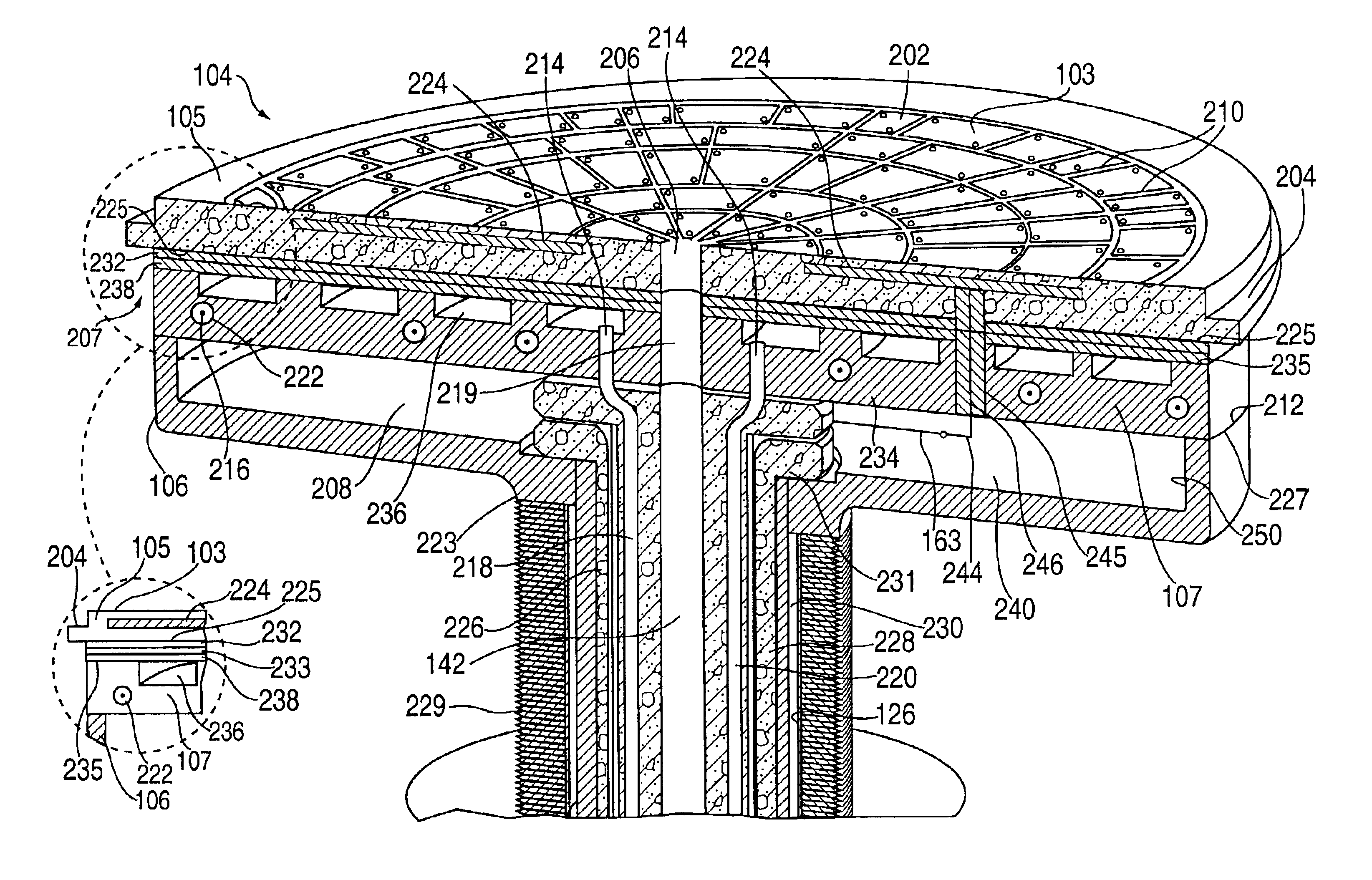
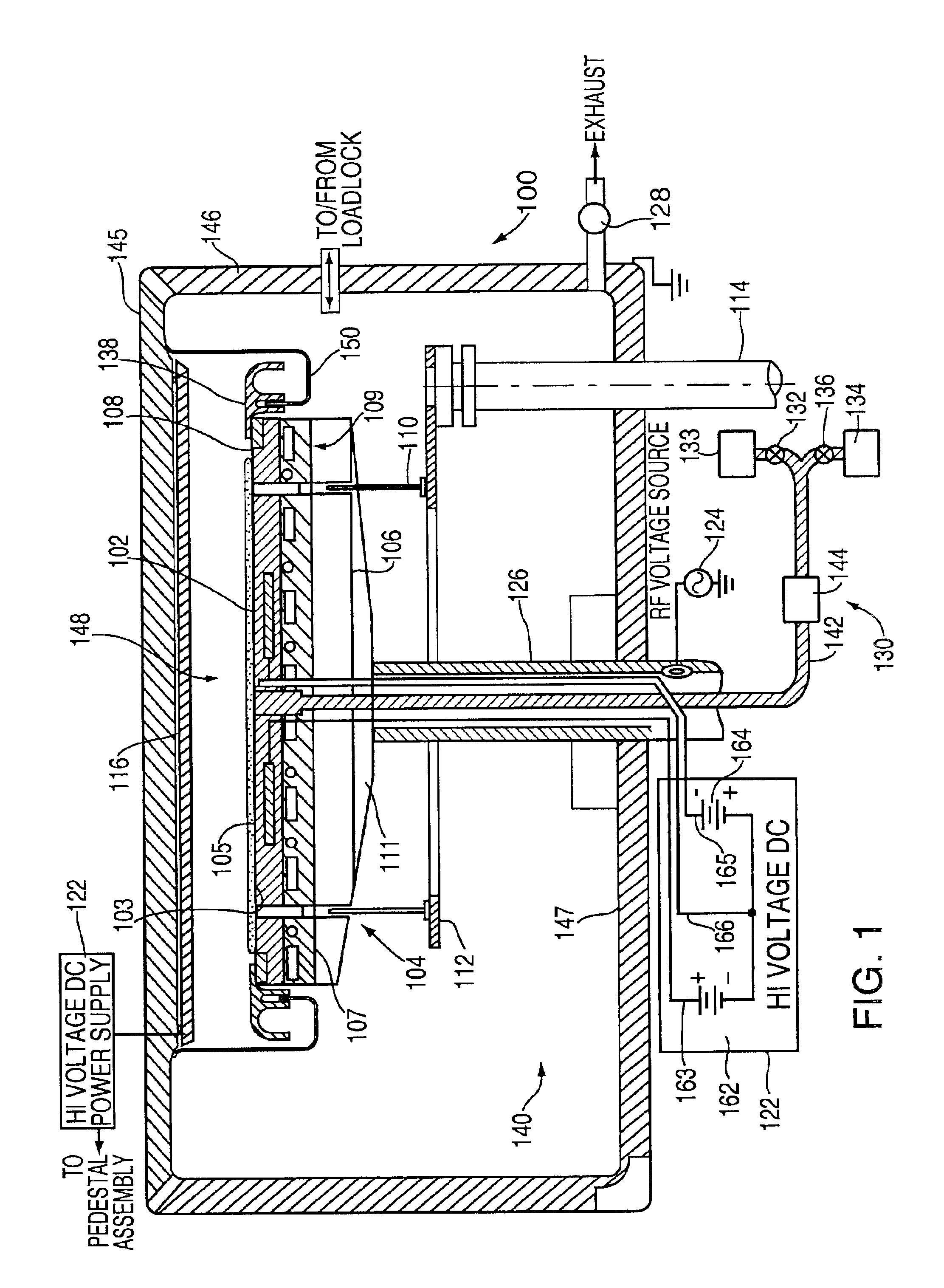
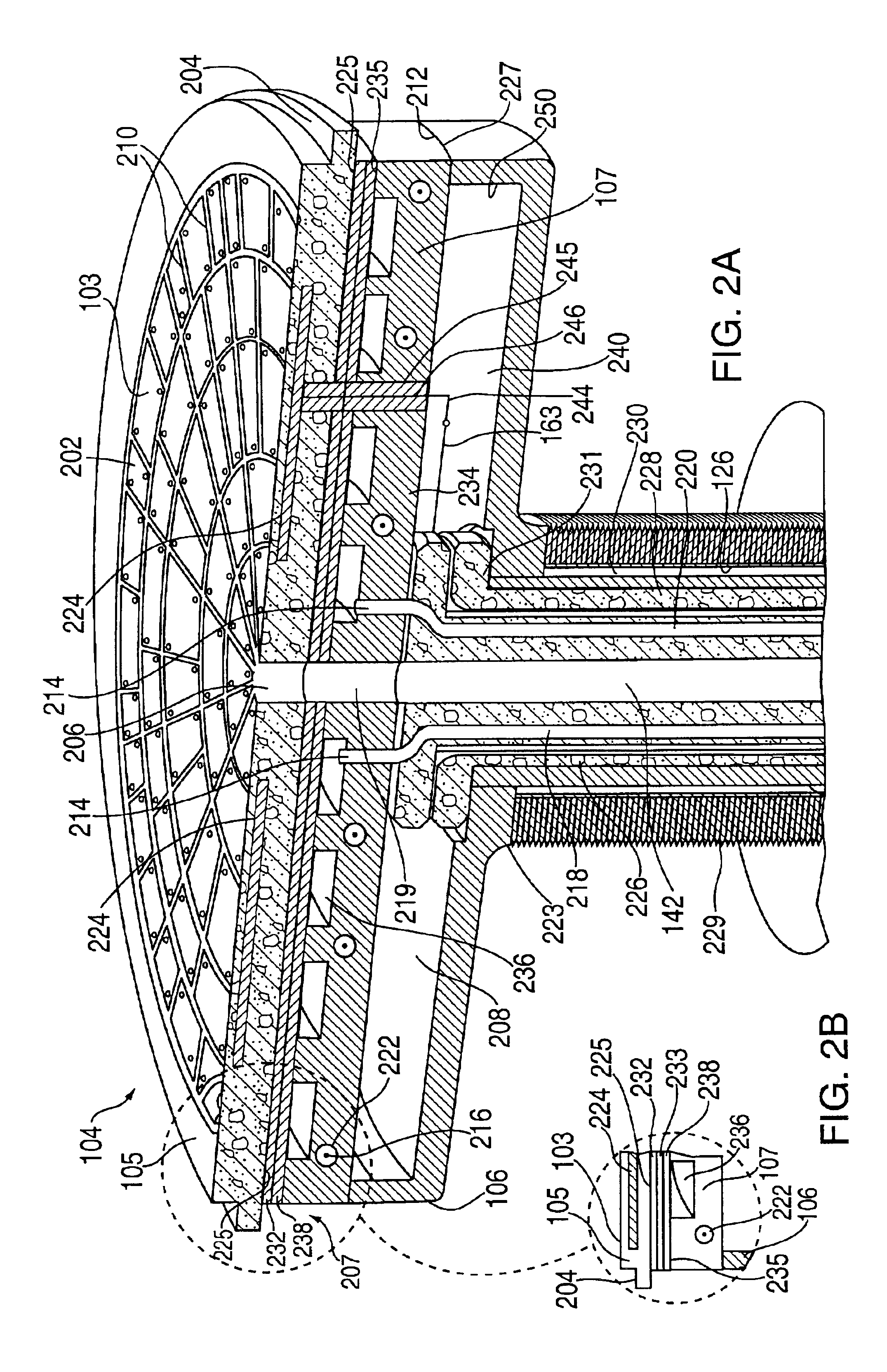
Full area temperature controlled electrostatic chuck and method of fabricating same
PatentInactiveUS6853533B2
Innovation
- A three-piece wafer support assembly is developed, where a ceramic puck is low-temperature brazed to a composite cooling plate structure, and a pedestal is electron-beam welded to a pedestal joining-ring, ensuring secure and uniform temperature control across the wafer surface.

Environmental Impact Assessment of Wafer Processing
The environmental implications of wafer processing, particularly in thermal expansion coefficient optimization during wafer reconstitution, present significant sustainability challenges that require comprehensive assessment. Traditional wafer processing methods consume substantial energy resources, primarily through high-temperature annealing processes and precision thermal cycling equipment necessary for achieving optimal thermal expansion matching between different materials.
Energy consumption represents the most substantial environmental impact in thermal expansion optimization processes. The repeated heating and cooling cycles required for stress relief and coefficient adjustment typically operate at temperatures ranging from 200°C to 400°C, consuming approximately 15-25% more energy compared to standard wafer processing. This increased energy demand directly correlates with higher carbon emissions, particularly in regions where electricity generation relies heavily on fossil fuels.
Chemical waste generation poses another critical environmental concern. The optimization process often requires specialized chemical treatments, including surface modification agents and stress-relief compounds, which generate hazardous byproducts. Approximately 30-40% of these chemicals become waste streams requiring specialized disposal methods, contributing to both water contamination risks and solid waste accumulation.
Water resource utilization in thermal expansion optimization processes significantly exceeds standard wafer processing requirements. The cooling systems necessary for precise temperature control consume an estimated 40-60% more deionized water, while chemical cleaning steps associated with thermal treatment generate contaminated wastewater requiring extensive treatment before discharge.
Material waste represents an often-overlooked environmental impact. The iterative nature of thermal expansion coefficient optimization results in higher rejection rates during initial process development, with approximately 15-20% of processed wafers failing to meet specifications. These rejected wafers contribute to electronic waste streams and represent embedded environmental costs from upstream manufacturing processes.
Emerging sustainable approaches focus on process optimization through advanced modeling and simulation techniques, reducing the need for physical iterations. Implementation of closed-loop cooling systems and solvent recovery processes shows promise for minimizing resource consumption. Additionally, the development of lower-temperature processing methods could significantly reduce energy requirements while maintaining thermal expansion coefficient precision, representing a pathway toward more environmentally sustainable wafer reconstitution processes.
Quality Standards for Semiconductor Packaging Processes
Quality standards for semiconductor packaging processes involving wafer reconstitution with optimized thermal expansion coefficients require comprehensive frameworks that address both material properties and manufacturing precision. These standards must establish clear metrics for coefficient of thermal expansion (CTE) matching between different materials in the reconstituted wafer stack, typically targeting CTE values within ±2 ppm/°C variance to prevent delamination and warpage issues during thermal cycling.
International standards organizations such as JEDEC and IPC have developed specific guidelines for thermal mechanical properties in advanced packaging. JEDEC Standard JESD22-B112 defines test methods for measuring CTE in packaging materials, while IPC-9701A provides performance requirements for adaptive and area array packages. These standards mandate temperature cycling tests from -55°C to +150°C with specific ramp rates and dwell times to validate thermal expansion behavior.
Material qualification standards require extensive characterization of reconstitution materials including molding compounds, adhesives, and substrate materials. The standards specify that CTE measurements must be conducted using thermomechanical analysis (TMA) with sample preparation protocols that mirror actual manufacturing conditions. Critical parameters include glass transition temperature effects, moisture absorption impacts, and long-term aging stability of thermal expansion properties.
Process control standards emphasize real-time monitoring capabilities during wafer reconstitution operations. Statistical process control (SPC) methodologies must track key variables such as cure temperature profiles, pressure application uniformity, and cooling rate management. Control limits are typically set at ±3 sigma levels with capability indices (Cpk) exceeding 1.33 for critical thermal expansion parameters.
Reliability qualification standards mandate accelerated testing protocols including temperature cycling, thermal shock, and high-temperature storage tests. These standards require demonstration of stable CTE behavior over minimum 1000 thermal cycles with failure criteria defined by specific warpage limits and interface integrity metrics. Documentation requirements include full traceability of material lots, process parameters, and measurement data to ensure reproducible quality outcomes in high-volume manufacturing environments.
Unlock deeper insights with PatSnap Eureka Quick Research — get a full tech report to explore trends and direct your research. Try now!
Generate Your Research Report Instantly with AI Agent
Supercharge your innovation with PatSnap Eureka AI Agent Platform!