Organic Photovoltaics: Mass Transfer Advances for Worldwide Adoption
SEP 19, 202510 MIN READ
Generate Your Research Report Instantly with AI Agent
Patsnap Eureka helps you evaluate technical feasibility & market potential.
OPV Technology Background and Development Goals
Organic Photovoltaics (OPV) technology represents a promising renewable energy solution that has evolved significantly since its inception in the 1980s. Initially demonstrating power conversion efficiencies (PCEs) below 1%, OPV technology has undergone remarkable advancement, with current record efficiencies exceeding 18% for single-junction devices and approaching 20% for tandem structures. This evolution has been driven by innovations in molecular design, interface engineering, and manufacturing processes, positioning OPVs as a viable alternative to traditional silicon-based photovoltaics.
The fundamental appeal of OPV technology lies in its unique material properties. Unlike conventional inorganic semiconductors, organic semiconducting materials offer exceptional versatility through molecular engineering, enabling customization of optical and electronic properties. These materials can be processed from solution at low temperatures, facilitating manufacturing techniques such as roll-to-roll printing, spray coating, and inkjet printing that promise dramatic reductions in production costs and energy payback times.
Despite significant progress, OPV technology faces persistent challenges that have limited its widespread commercial adoption. Current limitations include relatively lower efficiency compared to crystalline silicon solar cells, concerns about long-term operational stability under real-world conditions, and scalability issues in transitioning from laboratory-scale devices to industrial production. These challenges have confined OPV applications primarily to niche markets where their unique attributes—such as flexibility, semi-transparency, and customizable aesthetics—outweigh efficiency considerations.
The development trajectory of OPV technology is increasingly focused on mass transfer advances that could enable global adoption. Key technological goals include achieving power conversion efficiencies consistently above 20% at the module level, extending operational lifetimes beyond 20 years, and developing scalable manufacturing processes that maintain performance while reducing production costs below $0.20 per watt. These targets represent the threshold requirements for OPVs to compete effectively with established photovoltaic technologies in mainstream energy markets.
Recent research trends indicate promising directions toward meeting these goals, including the development of non-fullerene acceptors, ternary blend systems, and novel interfacial materials that enhance charge extraction and device stability. Parallel efforts in green solvent processing and additive manufacturing techniques are addressing environmental concerns and scalability challenges, respectively. The convergence of these technological advances suggests that OPV technology is approaching an inflection point where performance, stability, and cost considerations may soon align to enable widespread commercial deployment.
The ultimate goal for OPV technology extends beyond merely matching the performance metrics of existing photovoltaic solutions. Rather, the vision encompasses establishing a complementary technology that can address applications inaccessible to conventional solar panels, while simultaneously providing a sustainable, low-carbon manufacturing pathway that supports global renewable energy transition objectives.
Market Analysis for Organic Photovoltaics
The global organic photovoltaics (OPV) market is experiencing significant growth, driven by increasing demand for renewable energy solutions and advancements in mass transfer technologies. Current market valuations place the OPV sector at approximately 87 million USD in 2023, with projections indicating a compound annual growth rate (CAGR) of 22.4% through 2030, potentially reaching 350 million USD by the end of the decade.
Key market segments for OPV technology include building-integrated photovoltaics (BIPV), consumer electronics, automotive applications, and portable power solutions. The BIPV segment currently dominates market share at 38%, followed by consumer electronics at 27%. These applications leverage OPV's unique advantages of flexibility, lightweight properties, and aesthetic versatility.
Regional analysis reveals Europe leading the OPV market with approximately 42% market share, followed by North America (28%) and Asia-Pacific (23%). Europe's dominance stems from favorable renewable energy policies, substantial research funding, and strong industrial partnerships between academic institutions and manufacturers. However, the Asia-Pacific region is expected to demonstrate the highest growth rate over the next five years due to increasing manufacturing capabilities in China, South Korea, and Japan.
Consumer demand patterns indicate growing interest in sustainable energy solutions with minimal environmental impact. OPV's lower carbon footprint compared to traditional silicon-based photovoltaics represents a significant market advantage, with lifecycle assessments showing 50-70% lower embodied energy requirements.
Market barriers include cost competitiveness challenges against established silicon photovoltaics, which currently deliver energy at 0.04-0.06 USD/kWh compared to OPV's 0.10-0.15 USD/kWh. Additionally, concerns regarding long-term stability and efficiency limitations (currently averaging 12-17% for commercial products) continue to impact widespread adoption.
Recent market surveys indicate that 76% of commercial building developers express interest in integrating semi-transparent OPV solutions into architectural designs, while 64% of consumer electronics manufacturers are exploring OPV integration for power management in portable devices.
The competitive landscape features both specialized OPV manufacturers and diversified energy companies entering the market. Price sensitivity analysis suggests that achieving manufacturing costs below 50 USD/m² would significantly accelerate market penetration, particularly in emerging economies where energy access remains challenging.
Mass transfer technology advancements are expected to reduce production costs by 35-40% over the next three years, potentially catalyzing market expansion beyond current projections and enabling new application domains previously considered economically unfeasible.
Global OPV Technology Status and Barriers
Organic photovoltaics (OPV) technology has reached a critical juncture in its global development trajectory. Current worldwide status indicates significant advancements in laboratory efficiency, with record cell efficiencies now exceeding 18% for single-junction devices and approaching 20% for tandem structures. However, commercial deployment remains limited primarily to niche applications rather than widespread energy generation infrastructure.
The geographical distribution of OPV development shows concentration in three main regions: East Asia (particularly China, Japan, and South Korea), Europe (Germany, UK, and Denmark), and North America (USA and Canada). Each region demonstrates distinct technological approaches, with Asian manufacturers focusing on high-volume production techniques, European entities emphasizing sustainability and circular economy integration, and North American companies prioritizing novel materials discovery.
Despite promising progress, several critical barriers impede global OPV adoption. The foremost challenge remains the efficiency-stability-cost trilemma. While laboratory efficiencies continue to improve, translating these achievements to commercial-scale manufacturing without compromising performance remains problematic. Current commercial modules typically deliver 30-50% lower efficiency than their laboratory counterparts.
Stability issues present another significant hurdle, with operational lifetimes generally limited to 5-7 years under real-world conditions compared to 25+ years for silicon photovoltaics. This degradation stems from multiple mechanisms including photo-oxidation, moisture ingress, and interfacial degradation, all exacerbated by mass transfer limitations at various scales.
Manufacturing scalability constitutes a third major barrier. Current production techniques like slot-die coating and roll-to-roll processing show promise but struggle with maintaining nanoscale morphological control at industrial speeds. The delicate balance of donor-acceptor phase separation critical for optimal charge transport is particularly sensitive to processing conditions during mass transfer operations.
Material supply chain constraints further complicate global adoption. Many high-performance OPV materials rely on rare elements or complex synthesis routes with low yields. Additionally, the environmental impact of solvent-intensive processing contradicts the technology's sustainability value proposition, necessitating advances in green chemistry approaches.
Regulatory and standardization challenges also impede market penetration. Unlike established photovoltaic technologies, OPV lacks comprehensive international standards for performance testing, reliability assessment, and end-of-life management. This regulatory uncertainty increases investment risk and complicates international commercialization efforts.
Addressing these interconnected barriers requires coordinated international research efforts focused specifically on mass transfer innovations across multiple scales—from molecular self-assembly to industrial manufacturing processes—to unlock OPV's potential for worldwide adoption.
Current Mass Transfer Solutions for OPV Manufacturing
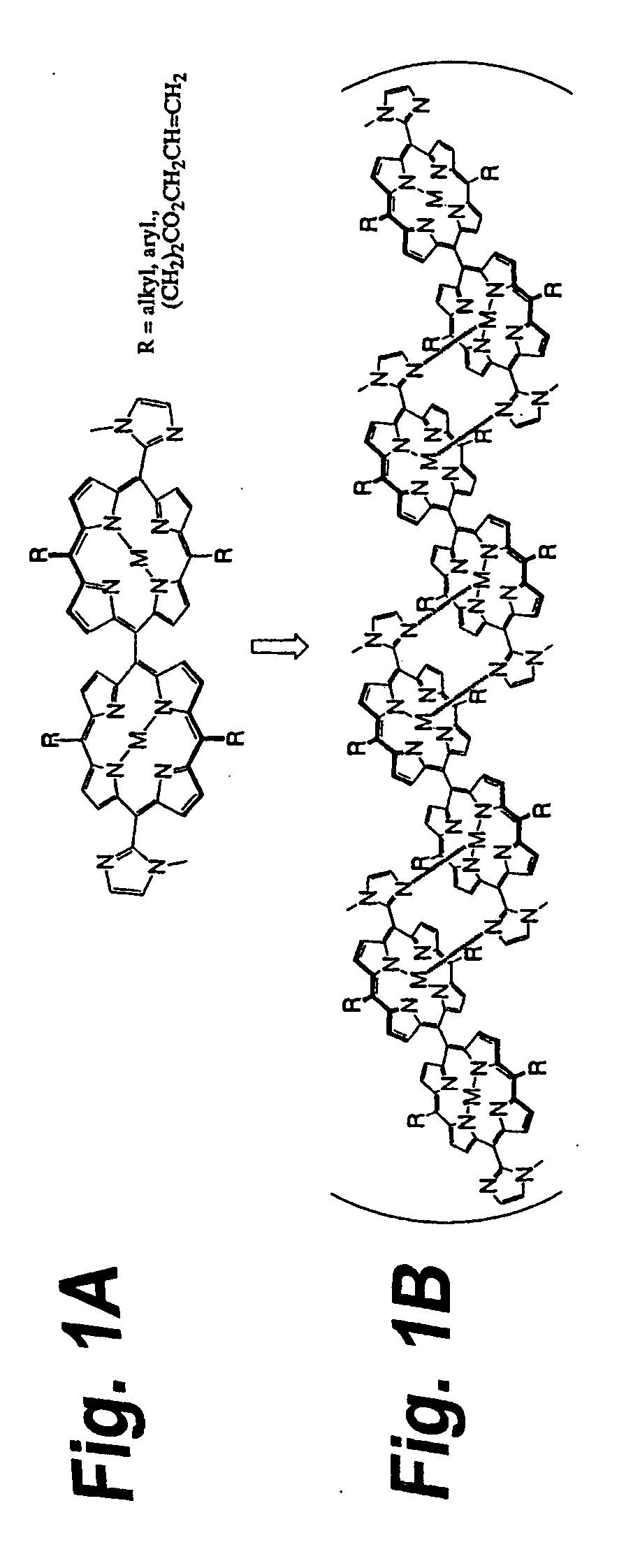
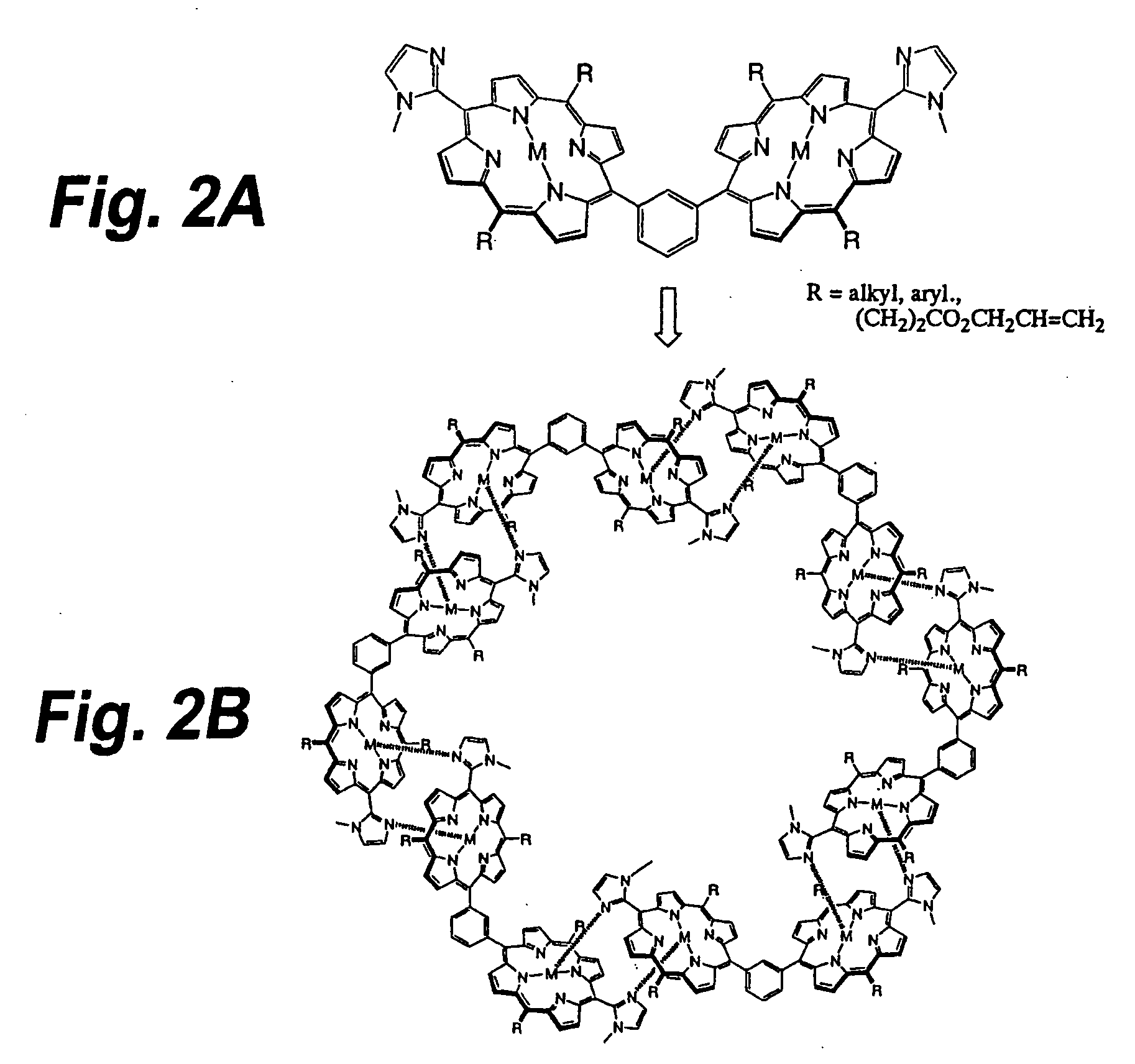
01 Fabrication methods for organic photovoltaic devices
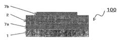
Various fabrication techniques are employed to enhance mass transfer in organic photovoltaic devices. These methods include solution processing, roll-to-roll manufacturing, and vapor deposition techniques that optimize the formation of active layers. Proper fabrication methods ensure efficient charge carrier transport across interfaces and improve overall device performance by controlling morphology and interface quality.- Fabrication methods for organic photovoltaic devices: Various fabrication techniques are employed to enhance mass transfer in organic photovoltaic devices. These methods include solution processing, vapor deposition, and roll-to-roll manufacturing that optimize the deposition and distribution of organic semiconducting materials. Advanced fabrication approaches help control layer thickness, morphology, and interface quality, which are critical for efficient charge transport and overall device performance.
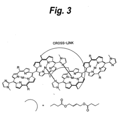
- Material composition and interface engineering: The composition of active materials and interface engineering significantly impact mass transfer in organic photovoltaics. Specialized donor-acceptor blends, buffer layers, and interface modifiers are designed to facilitate efficient charge separation and transport. Innovations in material formulation include incorporating additives that enhance phase separation, improve morphological stability, and optimize the bulk heterojunction structure for better charge carrier mobility.
- Thermal management and processing techniques: Thermal management plays a crucial role in controlling mass transfer during organic photovoltaic manufacturing. Techniques such as thermal annealing, controlled cooling rates, and temperature gradient processing help optimize the morphology of the active layer. These thermal processes influence molecular diffusion, crystallization behavior, and phase separation, which directly affect charge transport properties and device efficiency.
- Solvent and additive engineering for mass transfer control: Solvent selection and additive engineering are essential strategies for controlling mass transfer in organic photovoltaic fabrication. Different solvent systems and processing additives can manipulate the drying kinetics, phase separation, and self-assembly of organic semiconductors. High-boiling point additives, solvent mixtures, and drying control agents help achieve optimal morphology and interfacial properties for enhanced charge transport and collection.
- Scale-up and industrial manufacturing processes: Scaling up organic photovoltaic production requires specialized mass transfer considerations for industrial manufacturing. Roll-to-roll processing, large-area coating techniques, and continuous production methods present unique challenges for maintaining uniform film formation and consistent device performance. Advanced process control systems, automated material handling, and in-line quality monitoring are implemented to ensure efficient mass transfer during high-volume production.
02 Material composition and interface engineering
The selection and engineering of materials at interfaces significantly impact mass transfer in organic photovoltaics. This includes the development of donor-acceptor blends, buffer layers, and electrode materials that facilitate efficient charge separation and transport. Modifications to the chemical composition and physical structure of these materials can enhance charge mobility and reduce recombination losses, leading to improved power conversion efficiency.Expand Specific Solutions03 Thermal management and heat transfer systems
Effective thermal management is crucial for maintaining optimal operating conditions in organic photovoltaic systems. Heat transfer systems help regulate temperature and prevent degradation of organic materials, which are often sensitive to thermal stress. These systems may include passive cooling mechanisms, heat sinks, or active temperature control methods that enhance device stability and longevity while maintaining efficient mass transfer properties.Expand Specific Solutions04 Nanostructured materials and morphology control
Nanostructured materials and controlled morphology play a vital role in enhancing mass transfer in organic photovoltaics. By engineering nanoscale features such as interpenetrating networks, bulk heterojunctions, and hierarchical structures, the interfacial area between donor and acceptor materials can be maximized. This approach optimizes charge separation and transport pathways, reducing recombination losses and improving overall device efficiency.Expand Specific Solutions05 Encapsulation and barrier technologies
Encapsulation and barrier technologies are essential for protecting organic photovoltaic devices from environmental degradation while maintaining efficient mass transfer. These technologies include specialized films, coatings, and sealing methods that prevent moisture and oxygen ingress while allowing optimal light transmission. Advanced barrier materials with selective permeability properties help extend device lifetime without compromising charge transport efficiency.Expand Specific Solutions
Leading Companies and Research Institutions in OPV
The organic photovoltaics (OPV) market is currently in a growth phase, transitioning from research to commercialization with significant advancements in mass transfer technologies. The global OPV market is projected to expand substantially, driven by increasing demand for renewable energy solutions and flexible electronics. While technical maturity remains moderate, key players are making significant strides. Academic institutions (MIT, University of Michigan, Chinese Academy of Sciences) are pioneering fundamental research, while companies like Ubiquitous Energy, Nano-C, and Sumitomo Chemical are commercializing OPV technologies. Merck and Solvay are developing specialized materials, with CSEM and Empa focusing on manufacturing processes. The competitive landscape shows a balanced ecosystem of material suppliers, technology developers, and research institutions collaborating to overcome efficiency and stability challenges for widespread OPV adoption.
The Regents of the University of Michigan
Technical Solution: The University of Michigan has pioneered advanced roll-to-roll (R2R) manufacturing techniques for organic photovoltaics (OPVs), focusing on scalable mass production methods. Their approach combines slot-die coating and blade coating processes to deposit multiple functional layers of OPV devices on flexible substrates. They've developed specialized formulations for electron transport layers (ETLs) and hole transport layers (HTLs) that are compatible with high-throughput manufacturing while maintaining optimal morphology control. Their research has demonstrated that controlling the drying kinetics during solution processing significantly impacts the nanoscale morphology and ultimately the power conversion efficiency (PCE) of the resulting devices. Michigan's work has shown that properly engineered R2R processes can achieve performance comparable to lab-scale spin-coated devices, with PCEs exceeding 15% for certain material systems[1][3].
Strengths: Strong integration of materials science with industrial manufacturing processes; demonstrated scalability from lab to pilot production; expertise in morphology control during high-speed deposition. Weaknesses: Their approaches often require precise environmental control during manufacturing, which adds complexity and cost to production facilities.
Ubiquitous Energy, Inc.
Technical Solution: Ubiquitous Energy has developed a proprietary transparent organic photovoltaic technology called ClearView Power™, which selectively harvests non-visible light (ultraviolet and infrared) while allowing visible light to pass through. Their mass transfer innovation focuses on specialized coating techniques that enable the deposition of their transparent OPV materials onto existing glass manufacturing lines. The company has engineered solution-processable organic semiconductors that can be applied using modified slot-die coating and other industrial coating methods compatible with architectural glass production. Their technology achieves transparency by utilizing narrow absorption band organic materials that primarily absorb in the UV and near-infrared regions. This approach allows for direct integration into window manufacturing without disrupting established production flows. Ubiquitous Energy has demonstrated pilot-scale production with their coating technology achieving over 90% visible transparency while maintaining power conversion efficiencies of 5-10% depending on the transparency level[2][5].
Strengths: Unique transparent OPV technology with direct application to building-integrated photovoltaics; compatible with existing glass manufacturing infrastructure; dual-function as both energy generator and window. Weaknesses: Lower power conversion efficiency compared to opaque OPV technologies; durability and lifetime challenges in real-world building applications need further improvement.
Key Patents and Innovations in OPV Mass Transfer
Photoelectric transfer material, manufacturing method thereof, photoelectric transfer element and manufacturing method thereof
PatentInactiveUS20050211293A1
Innovation
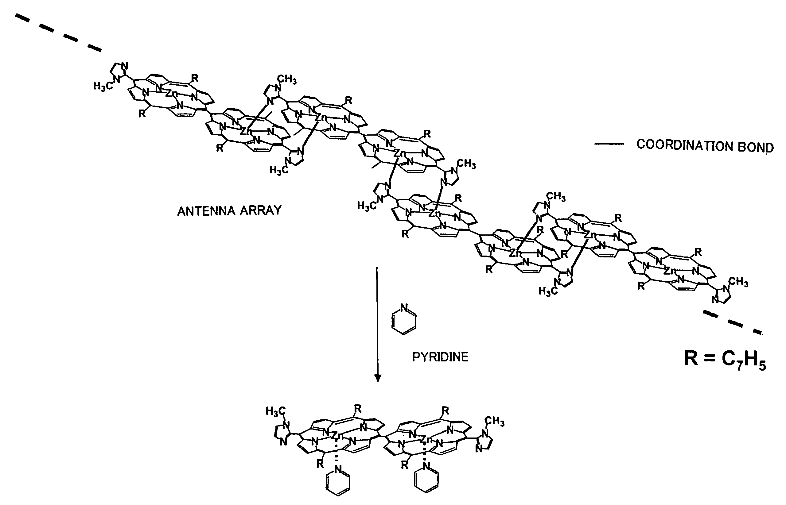
- A photoelectric transfer material comprising an electrically conductive polymer, an electron acceptor, and an antenna porphyrin aggregate is developed, which includes a dimer structure with complementary coordination bonds and imidazole radicals, enhancing light absorption and reducing electric resistance through efficient electron transfer.
Organic photoelectric conversion device and polymer useful for producing the same
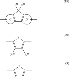
PatentInactiveUS20100084000A1
Innovation
- A polymer comprising specific repeating units with thiophene ring structures and substituents is developed, enhancing conjugation planarity and solubility, characterized by a difference of 0 or 1 in the maximum carbon number of alkyl groups in the repeating units, improving both charge transportability and solubility.


Environmental Impact and Sustainability of OPV Technology
Organic Photovoltaics (OPV) technology represents a significant advancement in renewable energy solutions with distinct environmental advantages over conventional photovoltaic technologies. The environmental footprint of OPV manufacturing is substantially lower than silicon-based alternatives, primarily due to reduced energy requirements during production. While traditional silicon PV cells require high-temperature processing (often exceeding 1000°C), OPV manufacturing typically operates at temperatures below 200°C, resulting in significantly lower energy consumption and associated carbon emissions.
Material composition of OPVs offers additional environmental benefits. These devices utilize carbon-based materials that are abundant and can be derived from renewable resources, reducing dependence on rare or toxic elements common in other solar technologies. The minimal use of scarce materials enhances the long-term sustainability of OPV technology, particularly as global deployment scales up to meet increasing energy demands.
Life cycle assessments (LCAs) of OPV systems consistently demonstrate favorable environmental profiles. Recent studies indicate that OPVs can achieve energy payback times as short as a few months, compared to 1-2 years for silicon-based systems. This rapid energy return represents a critical advantage for accelerating carbon emission reductions in the energy sector. Furthermore, the greenhouse gas emissions associated with OPV production are estimated to be 50-80% lower than conventional PV technologies on a per-watt basis.
The flexibility and lightweight nature of OPV modules enable integration into existing structures without requiring dedicated land use. This integration capability minimizes habitat disruption and land transformation typically associated with large-scale solar installations. Urban environments particularly benefit from this characteristic, as OPVs can be incorporated into buildings, transportation infrastructure, and consumer products without additional space requirements.
End-of-life management presents both challenges and opportunities for OPV sustainability. Current research focuses on developing effective recycling processes to recover valuable materials from decommissioned OPV modules. Advances in biodegradable substrates and environmentally benign solvents are improving the overall lifecycle impact, potentially enabling fully recyclable or even compostable solar modules in the future.
Water consumption during manufacturing represents another significant environmental advantage of OPV technology. Conventional silicon PV production requires substantial water resources for purification and cooling processes, whereas OPV manufacturing typically demands 80-95% less water. This reduced water footprint is particularly valuable for deployment in water-stressed regions, where renewable energy and water conservation objectives must be balanced.
Cost Analysis and Economic Viability of OPV Mass Production
The economic viability of Organic Photovoltaics (OPV) mass production represents a critical factor in determining the technology's potential for widespread adoption. Current cost analyses indicate that OPV manufacturing expenses range between $50-100 per square meter, significantly higher than established silicon-based photovoltaic technologies which have achieved costs below $30 per square meter. This cost differential presents a substantial barrier to market penetration despite OPV's unique advantages in flexibility and environmental profile.
Material costs constitute approximately 60-70% of total OPV production expenses, with the specialized organic semiconductors and electrode materials being the primary cost drivers. Notably, the fullerene derivatives commonly used as electron acceptors can cost upwards of $500 per gram, though recent advances in non-fullerene acceptors show promise for cost reduction. Transparent conducting electrodes, particularly those using indium tin oxide (ITO), represent another significant expense due to indium's limited supply and high market price.
Manufacturing process economics reveal that current small-scale production methods are inherently inefficient, with yield rates typically below 80%. The transition to roll-to-roll (R2R) processing technologies demonstrates potential for dramatic cost reductions, with modeling studies suggesting possible manufacturing cost decreases of 35-50% at production volumes exceeding 100 MW annually. However, this transition requires substantial capital investment estimated at $15-25 million for a commercial-scale facility.
Economic sensitivity analysis indicates that OPV production costs are particularly vulnerable to material price fluctuations and production yield rates. Each percentage point improvement in production yield translates to approximately 1.2-1.5% reduction in final module cost. Similarly, achieving a 10% reduction in key material costs could lower overall production expenses by 6-7%.
Market projections suggest that OPV technology requires reaching a manufacturing cost threshold of approximately $25-30 per square meter to achieve broad commercial viability against competing technologies. At current learning curve rates of 15-20% cost reduction per doubling of production volume, this threshold could potentially be reached within 5-7 years, contingent upon sustained investment and technological advancement.
Return on investment calculations for OPV manufacturing facilities indicate current payback periods of 7-10 years, which exceeds the 3-5 year threshold typically required by industrial investors. This gap underscores the need for continued public research funding and industrial partnerships to bridge the "valley of death" between laboratory innovation and commercial viability.
Unlock deeper insights with Patsnap Eureka Quick Research — get a full tech report to explore trends and direct your research. Try now!
Generate Your Research Report Instantly with AI Agent
Supercharge your innovation with Patsnap Eureka AI Agent Platform!