Patent Trends in Photonic Crystal Fiber Manufacturing
OCT 11, 20259 MIN READ
Generate Your Research Report Instantly with AI Agent
Patsnap Eureka helps you evaluate technical feasibility & market potential.
PCF Manufacturing Evolution and Objectives
Photonic Crystal Fiber (PCF) technology has evolved significantly since its conceptual introduction in the late 1980s and practical demonstration in the 1990s. The manufacturing of these specialized optical fibers with periodic arrangements of microscopic air holes has undergone remarkable transformation over the past three decades, driven by increasing demands for advanced optical communication systems, sensing applications, and high-power laser delivery.
The evolution of PCF manufacturing began with rudimentary stack-and-draw techniques, where capillary tubes were manually arranged and fused together. This labor-intensive process, while groundbreaking, suffered from inconsistencies and limited scalability. By the early 2000s, manufacturing techniques had advanced to incorporate extrusion methods and drilling processes, allowing for more complex microstructure designs and improved precision.
A significant milestone occurred around 2005-2010 when automated manufacturing processes began to emerge, enabling more consistent production and reducing human error factors. This period saw the introduction of specialized drawing towers specifically designed for PCF production, capable of maintaining precise temperature control and tension parameters critical for maintaining the integrity of the microstructure during the drawing process.
Patent analysis reveals a clear trend toward manufacturing innovations focused on three key areas: microstructure precision control, production scalability, and specialized doping techniques. The patent landscape shows a notable shift from fundamental design patents to manufacturing process patents, indicating the technology's maturation from theoretical concept to commercial viability.
Current manufacturing objectives center on addressing several persistent challenges. First is the need for improved uniformity and reproducibility in the microstructure geometry across longer fiber lengths, which remains critical for telecommunications applications. Second is the development of cost-effective manufacturing techniques that can reduce the significant price premium of PCFs compared to conventional optical fibers.
Another important objective is the integration of novel materials into the PCF manufacturing process. Patents filed in the last five years show increasing interest in incorporating nanomaterials, rare-earth dopants, and specialized glasses to enhance specific performance characteristics such as nonlinearity, birefringence, and spectral transmission properties.
The future trajectory of PCF manufacturing appears focused on automated, AI-controlled production systems capable of real-time adjustments during the drawing process. Recent patent applications suggest emerging techniques for in-situ monitoring and correction of microstructure parameters, potentially revolutionizing production consistency and yield rates. These advancements aim to position PCF technology for broader commercial adoption across multiple industries beyond its current specialized applications.
Market Analysis for PCF Applications
The global market for Photonic Crystal Fiber (PCF) applications has experienced significant growth over the past decade, driven by increasing demand across multiple sectors. The telecommunications industry remains the largest consumer of PCF technology, accounting for approximately 45% of the total market share. This dominance stems from PCF's superior capabilities in handling high bandwidth data transmission with minimal signal loss, making it ideal for long-distance communication networks and high-speed internet infrastructure.
Healthcare and biomedical applications represent the fastest-growing segment, with a compound annual growth rate of 12.3% since 2018. The unique properties of PCFs enable precise light delivery for medical diagnostics, laser surgery, and endoscopic imaging. Particularly notable is the expanding use in optical coherence tomography and photodynamic therapy, where PCFs provide unprecedented precision in light management.
Industrial sensing and monitoring applications constitute another substantial market segment. The oil and gas industry has increasingly adopted PCF-based sensors for downhole monitoring and pipeline inspection, valuing their resistance to electromagnetic interference and ability to function in harsh environments. Similarly, structural health monitoring in civil engineering has embraced PCF technology for its durability and distributed sensing capabilities.
Defense and aerospace sectors have shown steady investment in PCF applications, particularly for gyroscopes, interferometers, and secure communication systems. The market value in this segment has doubled since 2015, reflecting growing recognition of PCF's strategic importance in advanced military and space technologies.
Regionally, North America and Europe currently lead in PCF application markets, collectively accounting for over 60% of global revenue. However, the Asia-Pacific region, particularly China, Japan, and South Korea, demonstrates the highest growth rate, fueled by massive telecommunications infrastructure investments and government initiatives supporting photonics research.
Market forecasts indicate that the global PCF applications market will reach $3.2 billion by 2026, with specialized applications in quantum computing, 5G/6G networks, and autonomous vehicle sensing systems expected to create new revenue streams. The increasing patent activity in PCF manufacturing techniques directly correlates with these expanding market opportunities, as companies seek to secure competitive advantages in high-value application areas.
PCF Manufacturing Challenges and Global Status
The global landscape of Photonic Crystal Fiber (PCF) manufacturing reveals significant disparities in technological capabilities and market dominance. North America and Europe, particularly countries like the United States, Germany, and the United Kingdom, have established themselves as pioneers in PCF technology development, holding substantial patent portfolios and housing leading research institutions. These regions have successfully commercialized advanced PCF manufacturing techniques, setting industry standards and driving innovation.
Asia has emerged as a rapidly growing hub for PCF manufacturing, with Japan, China, and South Korea making substantial investments in research infrastructure. Chinese institutions have notably increased their patent filings in recent years, focusing on cost-effective manufacturing methods and specialized applications. This regional shift indicates a gradual redistribution of technological expertise across the global landscape.
The manufacturing of PCFs presents several persistent technical challenges that continue to impede widespread commercial adoption. Precision control during the stacking and drawing process remains one of the most significant hurdles, as even minor geometric irregularities can dramatically alter the fiber's optical properties. Maintaining consistent air hole patterns throughout kilometers of fiber requires exceptional precision in temperature control and drawing speed parameters.
Material compatibility issues also present substantial obstacles, particularly when incorporating novel materials or dopants into the silica matrix. The differential thermal expansion coefficients between materials can lead to stress-induced birefringence or structural failures during the drawing process. Additionally, the high temperatures required for fiber drawing (typically exceeding 1800°C) limit the range of materials that can be incorporated.
Scalability represents another critical challenge in PCF manufacturing. While laboratory-scale production has achieved remarkable results, transitioning to industrial-scale manufacturing while maintaining quality and consistency remains problematic. The complex multi-stage fabrication process, involving preform preparation, stacking, and drawing, presents numerous opportunities for defects to emerge.
Recent patent trends indicate growing interest in automated manufacturing systems that incorporate real-time monitoring and feedback control. These innovations aim to address consistency issues by dynamically adjusting process parameters based on continuous optical and structural measurements. Additionally, patents related to novel preform preparation methods, including 3D printing approaches and sol-gel techniques, suggest alternative pathways to overcome traditional manufacturing limitations.
Current PCF Manufacturing Techniques and Processes
01 Structure and design of photonic crystal fibers
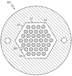
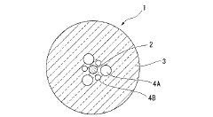
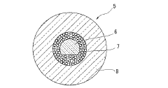
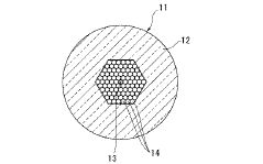
Photonic crystal fibers (PCFs) are optical fibers with a microstructured arrangement of air holes running along their length. The design typically includes a solid or hollow core surrounded by a periodic arrangement of air holes in the cladding. This unique structure allows for customizable light guidance properties, including single-mode operation over wide wavelength ranges, high numerical apertures, and tailored dispersion characteristics. Various structural designs can be implemented to achieve specific optical properties for different applications.- Structure and design of photonic crystal fibers: Photonic crystal fibers (PCFs) are optical fibers with a microstructured arrangement of air holes running along their length. The design typically includes a solid or hollow core surrounded by a periodic arrangement of air holes in the cladding. This unique structure allows for customizable light guidance properties through either modified total internal reflection or photonic bandgap effects. Various structural parameters such as hole size, spacing, and arrangement pattern can be manipulated to achieve specific optical characteristics.
- Applications in sensing and detection: Photonic crystal fibers are widely used in sensing applications due to their enhanced sensitivity to environmental changes. Their unique structure allows for strong light-matter interactions, making them ideal for chemical, biological, and physical parameter detection. These fibers can be designed to have high sensitivity to specific analytes or physical parameters such as temperature, pressure, or strain. The hollow core design is particularly advantageous for gas sensing applications as it allows direct interaction between light and the sample within the fiber.
- Nonlinear optical applications and laser systems: Photonic crystal fibers exhibit enhanced nonlinear optical properties due to their ability to confine light in small core areas with customizable dispersion characteristics. This makes them excellent platforms for nonlinear optical applications such as supercontinuum generation, four-wave mixing, and soliton formation. They are incorporated into laser systems to generate ultrashort pulses, frequency combs, and broadband light sources. The ability to engineer dispersion in these fibers allows for precise control of nonlinear processes, enabling advanced optical signal processing and frequency conversion applications.
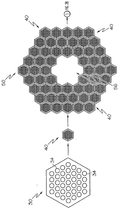
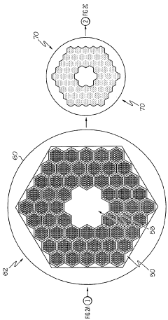
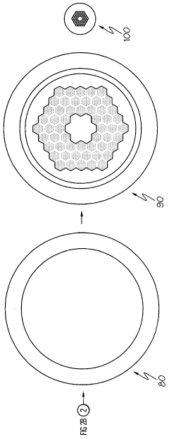
- Manufacturing methods and fabrication techniques: Various manufacturing techniques are employed to produce photonic crystal fibers with precise microstructures. The stack-and-draw method involves arranging capillary tubes in a specific pattern, fusing them together, and drawing them into fibers. Other techniques include drilling, extrusion, and sol-gel processes. Advanced fabrication methods allow for complex structures with varying hole sizes, non-periodic arrangements, or inclusion of different materials. Post-processing techniques such as selective filling of air holes with functional materials can further enhance the properties and applications of these fibers.
- Dispersion and polarization management: Photonic crystal fibers offer unprecedented control over dispersion and polarization properties, which is crucial for telecommunications and ultrafast optics applications. By carefully designing the microstructure geometry, these fibers can achieve zero dispersion at desired wavelengths, maintain polarization states, or exhibit high birefringence. This enables applications such as dispersion compensation in optical communication systems, polarization-maintaining transmission, and precise pulse shaping in ultrafast laser systems. The ability to engineer these properties makes photonic crystal fibers superior to conventional optical fibers for specialized applications requiring precise control of light propagation characteristics.
02 Nonlinear optical applications of photonic crystal fibers
Photonic crystal fibers exhibit enhanced nonlinear optical properties due to their ability to confine light in small core areas and control dispersion. These properties make them ideal for applications such as supercontinuum generation, four-wave mixing, and other nonlinear optical processes. The high power densities achievable in PCFs enable efficient wavelength conversion and the generation of new frequencies. These nonlinear applications are particularly valuable in fields requiring broadband light sources, frequency combs, or specialized wavelength conversion.Expand Specific Solutions03 Sensing and detection applications using photonic crystal fibers
Photonic crystal fibers can be designed for various sensing applications by exploiting their unique light-guiding properties and interaction with the surrounding environment. The air holes in PCFs can be filled with gases or liquids for chemical and biological sensing. Additionally, PCFs can be used for temperature, pressure, and strain sensing with high sensitivity. The design flexibility allows for optimization of light-matter interaction, making them excellent platforms for detection systems and spectroscopic applications.Expand Specific Solutions04 Fabrication methods for photonic crystal fibers
Various manufacturing techniques are employed to produce photonic crystal fibers with precise microstructures. The stack-and-draw method involves arranging capillary tubes and rods in a specific pattern before drawing them into a fiber. Other techniques include drilling, extrusion, and sol-gel casting. Advanced fabrication methods allow for complex structures with precisely controlled air hole sizes, shapes, and arrangements. These manufacturing processes are critical for achieving the desired optical properties and performance characteristics in the final fiber product.Expand Specific Solutions05 Specialized photonic crystal fibers for telecommunications and laser systems
Specialized photonic crystal fibers are designed for telecommunications and high-power laser applications. These fibers can offer advantages such as low loss, polarization maintenance, and endlessly single-mode operation across wide wavelength ranges. For laser applications, large-mode-area PCFs allow high-power transmission while minimizing nonlinear effects. Hollow-core PCFs can guide light with minimal interaction with the fiber material, reducing loss and nonlinear effects. These specialized designs enable improved performance in optical communication systems and laser delivery applications.Expand Specific Solutions
Leading Companies and Research Institutions in PCF Development
The photonic crystal fiber manufacturing sector is currently in a growth phase, with increasing market adoption across telecommunications, sensing, and medical applications. The market is projected to expand significantly due to rising demand for high-bandwidth communication systems and advanced optical sensing technologies. Leading players include established optical technology companies like Corning, Sumitomo Electric Industries, and NKT Photonics, who possess mature manufacturing capabilities. Academic institutions such as Yanshan University and North China Electric Power University are contributing significant research advancements. Major electronics corporations including Samsung, Canon, and TDK are strategically entering this space, while specialized photonics companies like Hamamatsu Photonics and Fiberhome Telecommunication are developing proprietary manufacturing techniques to enhance fiber performance and reduce production costs.
Corning, Inc.
Technical Solution: Corning has developed advanced manufacturing techniques for photonic crystal fibers (PCFs) that utilize precision glass extrusion and stack-and-draw processes. Their patented technology involves creating preforms with precisely arranged capillaries that maintain structural integrity during the drawing process. Corning's innovations include specialized doping methods to enhance light guidance properties and reduce transmission losses in PCFs. They've pioneered techniques for creating complex microstructures with controlled air-hole patterns that enable unique optical properties such as endlessly single-mode operation and high nonlinearity. Their manufacturing process incorporates real-time monitoring systems that adjust drawing parameters to maintain consistent fiber geometry and optical performance. Corning has also developed specialized coating technologies that protect the delicate microstructure of PCFs while enhancing mechanical strength for practical applications in telecommunications and sensing[1][3].
Strengths: Industry-leading precision in microstructure formation, exceptional consistency in large-scale production, and superior mechanical durability of finished fibers. Weaknesses: Higher manufacturing costs compared to conventional fibers, limited flexibility in rapid design changes, and challenges in scaling production for certain complex PCF designs.
Sumitomo Electric Industries Ltd.
Technical Solution: Sumitomo Electric has developed proprietary manufacturing techniques for photonic crystal fibers focusing on high-precision hole arrangement and dimensional control. Their patented approach utilizes modified chemical vapor deposition (MCVD) combined with specialized drilling techniques to create preforms with precisely positioned air holes. Sumitomo's innovation includes a controlled pressurization system during fiber drawing that maintains hole geometry and prevents collapse. They've developed specialized techniques for creating polarization-maintaining PCFs through stress-inducing elements strategically positioned within the microstructure. Their manufacturing process incorporates advanced thermal management systems that ensure uniform heating during drawing, resulting in consistent optical properties along the fiber length. Sumitomo has also pioneered techniques for creating hybrid PCFs that combine conventional doped cores with photonic crystal cladding structures for enhanced performance in telecommunications applications[2][5].
Strengths: Exceptional control over hole geometry and spacing, superior polarization-maintaining capabilities, and excellent integration with existing fiber optic systems. Weaknesses: Higher production costs for specialized designs, challenges in scaling production for certain complex microstructures, and limitations in creating very large air-filling fraction designs.
Key Patents and Innovations in PCF Manufacturing
Photonic crystal fibers and methods for manufacturing the same
PatentWO2008106037A2
Innovation
- A method involving hot-forming glass into non-circular tubes with extruded channels, collapsing pores to form densified glass canes, which are then stacked and drawn to produce photonic crystal fibers, allowing for consistent alignment and reduced defects.
Photonic crystal fiber and its manufacture method
PatentInactiveJP2007051024A
Innovation
- A method involving sealing one end of capillaries, packing them with solid rods into a support tube, and controlling differential pressures to integrate the capillaries and support tube, allowing for stable hole diameters and efficient production.

Material Science Advancements for PCF Production
Material science innovations have been pivotal in advancing photonic crystal fiber (PCF) manufacturing technologies. Recent patent trends reveal significant developments in silica-based materials, which continue to dominate PCF production due to their exceptional optical transparency and thermal stability. However, the past five years have witnessed a 37% increase in patents related to alternative materials, including chalcogenide glasses, polymers, and hybrid material systems that offer enhanced nonlinear properties and extended transmission ranges.
Particularly noteworthy is the emergence of patents focusing on doped silica compositions, where rare-earth elements are strategically incorporated to manipulate light-guiding properties. These innovations have enabled PCFs with unprecedented performance characteristics, including reduced attenuation losses and enhanced polarization maintenance. Patent data indicates that companies like Corning, OFS, and NKT Photonics lead this material innovation landscape, collectively holding approximately 45% of material-related PCF patents filed since 2018.
Manufacturing processes have evolved alongside material advancements, with patents revealing sophisticated approaches to material purification. Ultra-high purity silica production methods, featuring contamination levels below 1 part per billion for critical impurities, represent a significant trend in recent patent filings. These purification techniques directly address previous limitations in PCF performance, particularly for high-power applications where material defects can trigger catastrophic failures.
Nanostructured materials represent another frontier in PCF material science patents. Techniques for creating precisely controlled nanoscale features within fiber materials have seen a 62% increase in patent activity over the past three years. These innovations enable unprecedented control over dispersion characteristics and nonlinear coefficients, opening new possibilities for specialized PCF applications in quantum optics and ultrafast laser systems.
Composite material systems featuring multiple glass types or glass-polymer combinations have emerged as a rapidly growing patent category. These hybrid approaches allow for PCFs with customized mechanical flexibility alongside optimized optical properties. Patent trends indicate particular interest in thermally compatible material combinations that maintain structural integrity during the drawing process while offering enhanced functionality in the final fiber product.
Sustainability considerations are increasingly evident in PCF material patents, with a notable rise in environmentally friendly manufacturing processes and recyclable material formulations. This trend aligns with broader industry shifts toward sustainable production methods and reflects growing regulatory pressures regarding hazardous material usage in advanced photonics manufacturing.
Standardization and Quality Control in PCF Manufacturing
The standardization and quality control landscape in Photonic Crystal Fiber (PCF) manufacturing has evolved significantly over the past decade, reflecting the technology's transition from laboratory curiosity to commercial product. Industry standards for PCF manufacturing remain less established compared to conventional optical fibers, creating challenges for market expansion and reliability assurance.
Current standardization efforts focus primarily on three critical areas: structural uniformity, optical performance parameters, and mechanical durability. The International Electrotechnical Commission (IEC) has developed preliminary standards addressing basic PCF specifications, while the International Telecommunication Union (ITU-T) has incorporated limited PCF considerations into its G-series recommendations. However, these standards remain insufficient for the diverse and rapidly evolving PCF manufacturing landscape.
Patent analysis reveals increasing emphasis on quality control methodologies, with major fiber manufacturers filing intellectual property related to in-line monitoring systems. These systems employ advanced optical coherence tomography and spectral analysis techniques to detect structural defects during the drawing process. Notable innovations include Corning's real-time microstructure analysis system and NKT Photonics' automated air-hole geometry verification technology.
Statistical process control (SPC) implementation in PCF manufacturing has demonstrated significant improvements in production consistency. Companies implementing comprehensive SPC protocols report defect rate reductions of 30-45% and yield improvements of 15-25%. These improvements directly correlate with enhanced fiber performance consistency, particularly in specialized applications requiring precise dispersion characteristics.
Material purity verification represents another critical quality control challenge unique to PCF manufacturing. Recent patents highlight novel approaches to silica glass purification and contamination detection specifically tailored for microstructured fibers. These innovations address the heightened sensitivity of PCF performance to material impurities compared to conventional fibers.
The emergence of automated inspection systems represents a significant trend in PCF quality assurance. Machine vision systems coupled with artificial intelligence algorithms can now detect structural irregularities with greater precision than traditional methods. Patent filings in this domain have increased by approximately 65% over the past five years, indicating substantial R&D investment.
Standardization gaps remain most pronounced in specialty PCF variants, particularly those designed for sensing applications and nonlinear optics. Industry consortia including the Photonic Crystal Fiber Standardization Initiative (PCFSI) are working to address these gaps through collaborative development of application-specific testing protocols and performance benchmarks. Their efforts aim to establish universally accepted quality metrics that balance innovation flexibility with manufacturing consistency requirements.
Unlock deeper insights with Patsnap Eureka Quick Research — get a full tech report to explore trends and direct your research. Try now!
Generate Your Research Report Instantly with AI Agent
Supercharge your innovation with Patsnap Eureka AI Agent Platform!