Photo Imageable Dielectrics: High Density Application Techniques
APR 3, 20269 MIN READ
Generate Your Research Report Instantly with AI Agent
PatSnap Eureka helps you evaluate technical feasibility & market potential.
Photo Imageable Dielectric Technology Background and Objectives
Photo Imageable Dielectrics (PID) technology emerged in the 1980s as a revolutionary approach to address the growing complexity of electronic packaging and interconnect systems. Initially developed to overcome limitations of traditional dielectric materials in multilayer circuit boards, PID technology has evolved from simple photopolymer applications to sophisticated high-density interconnect solutions. The technology leverages photolithographic processes similar to semiconductor manufacturing, enabling precise patterning of dielectric layers with micron-level accuracy.
The fundamental principle behind PID technology involves the use of photosensitive polymer materials that can be selectively exposed, developed, and cured to create three-dimensional dielectric structures. This approach eliminates the need for mechanical drilling and traditional subtractive processes, significantly reducing manufacturing complexity and enabling higher interconnect densities. The technology has progressed through several generations, from early benzocyclobutene-based systems to advanced polyimide and hybrid organic-inorganic formulations.
The primary objective of modern PID technology centers on achieving ultra-high density interconnects while maintaining superior electrical performance and reliability. Key technical goals include minimizing dielectric constant and loss tangent values to support high-frequency applications, achieving aspect ratios exceeding 10:1 for via structures, and enabling feature sizes below 10 micrometers. These objectives are driven by the relentless demand for miniaturization in consumer electronics, telecommunications infrastructure, and advanced computing systems.
Contemporary PID development focuses on addressing thermal management challenges, as higher interconnect densities generate increased heat dissipation requirements. Advanced formulations incorporate thermally conductive fillers and engineered polymer matrices to achieve thermal conductivities approaching 2 W/mK while preserving electrical insulation properties. Additionally, the technology aims to achieve coefficient of thermal expansion matching with substrate materials to prevent stress-induced failures during thermal cycling.
The strategic importance of PID technology extends beyond traditional printed circuit board applications into emerging fields such as system-in-package solutions, flexible electronics, and three-dimensional integrated circuits. Future objectives include developing environmentally sustainable formulations that eliminate hazardous solvents and reduce processing temperatures, while simultaneously improving mechanical properties and long-term reliability under harsh operating conditions.
Market Demand for High Density Electronic Packaging
The global electronics industry is experiencing unprecedented demand for miniaturization and performance enhancement, driving significant market requirements for high-density electronic packaging solutions. This trend is particularly pronounced in consumer electronics, automotive systems, telecommunications infrastructure, and aerospace applications where space constraints and performance demands continue to intensify.
Consumer electronics represent the largest market segment driving high-density packaging demand. Smartphones, tablets, wearables, and IoT devices require increasingly compact form factors while delivering enhanced functionality. The proliferation of 5G technology has further accelerated this demand, as devices must accommodate additional RF components, antennas, and processing units within existing or smaller footprints.
The automotive sector presents rapidly expanding opportunities for high-density packaging technologies. Electric vehicles, autonomous driving systems, and advanced driver assistance systems require sophisticated electronic control units that must operate reliably in harsh environments while maintaining compact dimensions. The integration of multiple sensors, processors, and communication modules within limited vehicle space creates substantial demand for advanced packaging solutions.
Data center and cloud computing infrastructure constitute another major demand driver. Server processors, memory modules, and networking equipment require exceptional thermal management and electrical performance in increasingly dense configurations. The growing computational demands of artificial intelligence and machine learning applications further intensify requirements for high-performance, high-density packaging solutions.
Telecommunications equipment manufacturers face mounting pressure to deliver enhanced network capacity and speed while reducing equipment footprint and power consumption. Base stations, network switches, and optical communication systems require advanced packaging technologies to achieve required performance levels within space and thermal constraints.
The aerospace and defense sectors demand high-density packaging solutions that can withstand extreme environmental conditions while maintaining reliability and performance. Satellite systems, avionics, and military electronics require miniaturized components with exceptional durability and long-term stability.
Market growth is further supported by emerging applications in medical devices, industrial automation, and renewable energy systems. These sectors increasingly require compact, high-performance electronic systems that can operate reliably in demanding environments while meeting stringent regulatory requirements.
Current State and Challenges of PID High Density Applications
Photo Imageable Dielectrics (PID) technology has reached a critical juncture in its evolution toward high-density applications, with current implementations demonstrating both significant achievements and persistent limitations. The technology has successfully enabled feature sizes down to 10-15 micrometers in production environments, supporting the miniaturization demands of advanced electronic packaging and semiconductor applications.
Contemporary PID formulations primarily utilize negative-tone photoresist chemistry, incorporating acrylate-based polymers with photoinitiator systems optimized for i-line and broadband UV exposure. Leading manufacturers have achieved dielectric constants ranging from 3.0 to 4.2, with loss tangents below 0.02 at frequencies up to 10 GHz. These materials demonstrate excellent adhesion to copper substrates and maintain thermal stability up to 260°C during reflow processing.
However, several technical challenges continue to impede the advancement toward ultra-high-density applications. Resolution limitations become increasingly pronounced below 8-micrometer features, where sidewall roughness and dimensional control deteriorate significantly. The inherent trade-off between photosensitivity and mechanical properties constrains optimization efforts, as enhanced photospeed often compromises film integrity and adhesion performance.
Processing window constraints represent another critical challenge, particularly in high-volume manufacturing environments. Current PID systems exhibit narrow exposure latitude, typically ±15% for acceptable feature fidelity, which demands precise process control and limits manufacturing flexibility. Temperature sensitivity during post-exposure bake processes further complicates production scalability.
Reliability concerns emerge prominently in high-density configurations, where reduced spacing between conductive features increases susceptibility to moisture absorption and subsequent dielectric breakdown. Current materials demonstrate water uptake rates of 0.8-1.5% under standard environmental conditions, potentially compromising long-term electrical performance in demanding applications.
The geographical distribution of PID technology development reveals concentration in East Asian markets, particularly Taiwan, South Korea, and Japan, where advanced packaging requirements drive innovation. However, supply chain dependencies and limited material supplier diversity create potential vulnerabilities for global adoption.
Manufacturing cost considerations present additional obstacles, as high-density PID processing requires specialized equipment and extended processing cycles compared to conventional dielectric solutions. The economic viability threshold for widespread adoption remains challenging, particularly for cost-sensitive consumer electronics applications where performance benefits must justify premium pricing.
Existing High Density PID Application Solutions
01 Low-density photoimageable dielectric compositions
Photoimageable dielectric materials can be formulated with reduced density by incorporating hollow microspheres, porous fillers, or low-density additives. These compositions maintain photoimageability while achieving lower overall density, which is beneficial for reducing weight in electronic applications and improving thermal insulation properties. The density reduction can be achieved through careful selection of polymer matrices and filler materials that create void spaces within the cured dielectric layer.- Low-density photoimageable dielectric compositions: Photoimageable dielectric compositions can be formulated with reduced density by incorporating hollow microspheres, porous fillers, or low-density additives. These materials help decrease the overall density while maintaining photoimageability and dielectric properties. The reduced density is beneficial for applications requiring lightweight materials in electronic packaging and semiconductor devices.
- High-density photoimageable dielectric materials: Photoimageable dielectric materials with increased density can be achieved by incorporating high-density inorganic fillers such as barium titanate, silica, or ceramic particles. These formulations provide enhanced mechanical strength, improved thermal conductivity, and better dimensional stability. The higher density contributes to superior performance in multilayer circuit boards and advanced packaging applications.
- Density control through filler particle size distribution: The density of photoimageable dielectric materials can be precisely controlled by optimizing the particle size distribution of fillers. Using bimodal or multimodal particle size distributions allows for better packing efficiency, which directly affects the final density. This approach enables tailoring of material properties to meet specific application requirements while maintaining photoimaging capabilities.
- Density measurement and characterization methods: Various techniques are employed to measure and characterize the density of photoimageable dielectric materials, including pycnometry, buoyancy methods, and cross-sectional analysis. Accurate density measurement is critical for quality control and ensuring consistent performance in manufacturing processes. These characterization methods help correlate density with other material properties such as dielectric constant and mechanical strength.
- Density optimization for specific applications: Photoimageable dielectric materials can be formulated with optimized density ranges for specific applications such as high-frequency circuits, flexible electronics, or three-dimensional packaging. The density is adjusted by balancing the ratio of organic and inorganic components, controlling processing conditions, and selecting appropriate photoactive compounds. This optimization ensures the material meets both electrical performance and mechanical requirements for the intended application.
02 High-density photoimageable dielectric formulations
Increasing the density of photoimageable dielectrics can be accomplished by incorporating high-density inorganic fillers such as barium titanate, silica, or ceramic particles. These formulations provide enhanced mechanical strength, improved dimensional stability, and better electrical properties. The higher density materials are particularly useful in applications requiring robust dielectric layers with superior performance characteristics in multilayer circuit boards and semiconductor packaging.Expand Specific Solutions03 Density control through polymer resin selection
The base polymer resin system significantly influences the final density of photoimageable dielectrics. Selection of epoxy resins, acrylic polymers, or polyimide-based systems with different molecular weights and cross-linking densities allows for precise density control. The choice of photoinitiators and cross-linking agents also affects the final density by controlling the degree of polymerization and network formation during the photoimaging process.Expand Specific Solutions04 Filler loading optimization for density adjustment
The concentration and type of fillers incorporated into photoimageable dielectric compositions directly impact the material density. Optimization of filler loading levels, particle size distribution, and surface treatment of fillers enables precise density targeting. Various inorganic and organic fillers can be combined to achieve desired density ranges while maintaining processability and photoimaging characteristics. The filler-to-resin ratio is a critical parameter in controlling both density and other physical properties.Expand Specific Solutions05 Density measurement and characterization methods
Accurate measurement of photoimageable dielectric density is essential for quality control and process optimization. Various techniques including pycnometry, buoyancy methods, and cross-sectional analysis are employed to determine density values. The density can be measured at different stages of processing, including uncured, partially cured, and fully cured states. Characterization methods also assess density uniformity across the dielectric layer and its correlation with other properties such as dielectric constant and mechanical strength.Expand Specific Solutions
Key Players in PID and Advanced Packaging Industry
The photo imageable dielectrics market for high-density applications represents a mature yet evolving sector within the semiconductor and electronics manufacturing industry. The market demonstrates substantial scale, driven by increasing miniaturization demands in consumer electronics, automotive systems, and advanced packaging technologies. Key players span diverse technological capabilities, from established chemical giants like Dow Global Technologies and DuPont to specialized semiconductor equipment manufacturers including Applied Materials and Taiwan Semiconductor Manufacturing Company. Technology maturity varies significantly across the competitive landscape, with companies like Intel, Samsung Electronics, and FUJIFILM Corporation leading advanced photolithography innovations, while materials specialists such as JSR Corporation and Cabot Corporation focus on next-generation dielectric formulations. The sector benefits from strong R&D foundations through partnerships with institutions like Technical University of Denmark and Naval Research Laboratory, indicating robust innovation pipelines for emerging high-density interconnect solutions.
FUJIFILM Corp.
Technical Solution: FUJIFILM has leveraged their extensive photographic and imaging expertise to develop advanced photo imageable dielectric materials for electronic packaging applications. Their PID formulations utilize proprietary photopolymer chemistry derived from their film and imaging technologies, enabling high-resolution patterning with excellent edge definition and minimal sidewall roughness. The company's materials are specifically designed for high-density applications requiring fine-pitch features, offering superior adhesion properties and thermal stability up to 260°C processing temperatures. FUJIFILM's PID solutions support various packaging formats including flip-chip, wafer-level packaging, and flexible electronics, with particular strength in applications requiring precise thickness control and uniform coating properties across large substrate areas.
Strengths: Strong photochemistry expertise, excellent material uniformity, proven imaging technology heritage. Weaknesses: Smaller market presence compared to specialized semiconductor materials suppliers, limited equipment ecosystem partnerships.
Samsung Electronics Co., Ltd.
Technical Solution: Samsung has developed proprietary photo imageable dielectric technologies primarily for their advanced memory and logic packaging solutions. Their PID processes enable high-density interconnect structures for 3D memory stacking and system-in-package (SiP) applications, with demonstrated capabilities for sub-10μm via formation and fine-pitch redistribution layers. The company's approach integrates advanced materials with optimized lithography processes, achieving excellent step coverage and gap-fill properties essential for complex 3D structures. Samsung's PID technology supports their HBM (High Bandwidth Memory) packaging and advanced processor packaging requirements, incorporating low-k dielectric properties to minimize signal interference while maintaining mechanical reliability under thermal cycling conditions.
Strengths: Vertical integration advantages, strong R&D investment, proven performance in high-volume production. Weaknesses: Limited external availability of proprietary technologies, focus primarily on internal applications.
Core Innovations in PID High Density Processing Techniques
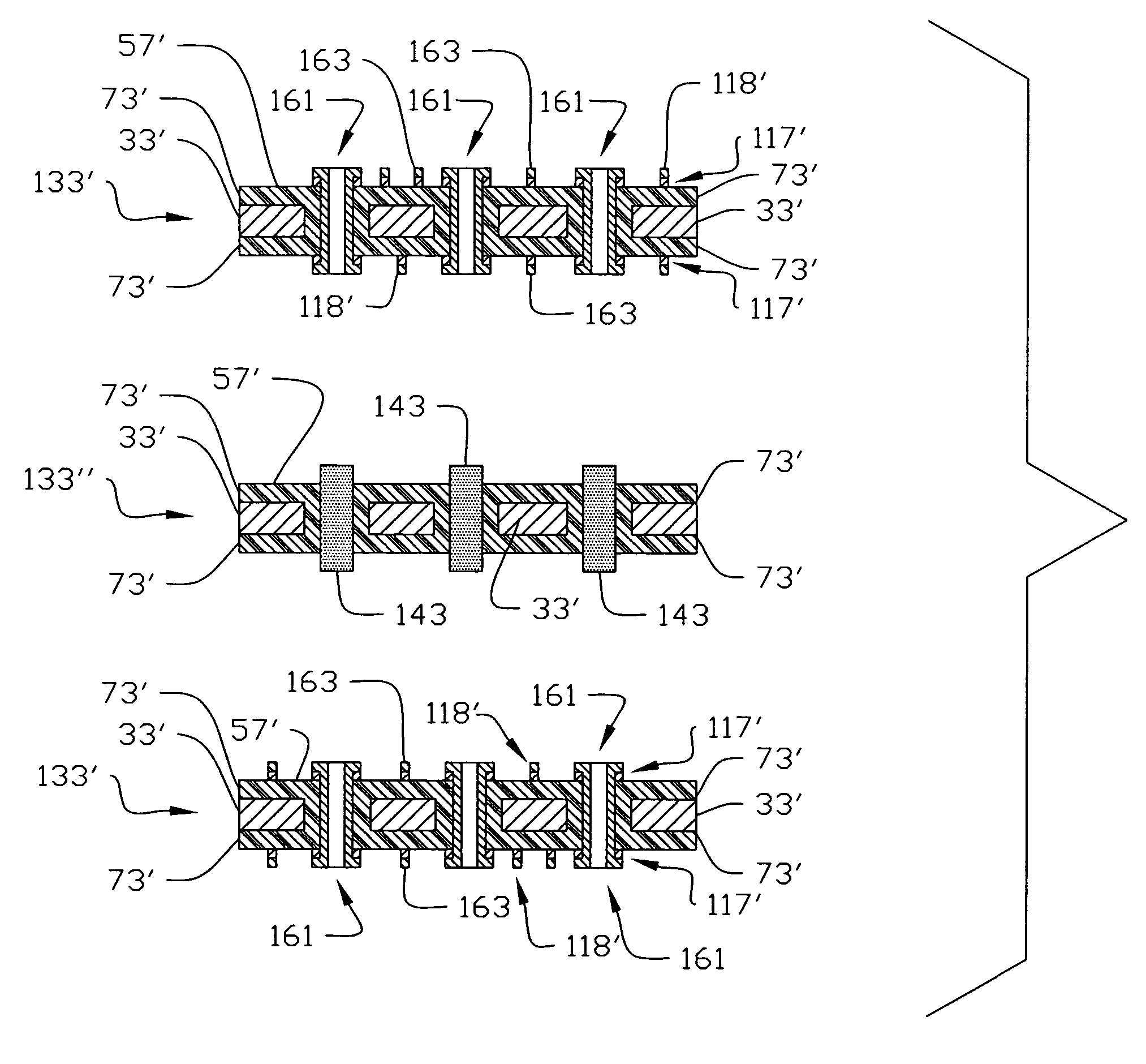
Inlay With Exposed Porous Layer, Component Carrier and Manufacturing Methods
PatentActiveUS20230309236A1
Innovation
- An inlay comprising a gas-permeable porous layer structure, an upper dielectric layer with cavities, and a metal layer is integrated into the component carrier, enabling airflow and protection while providing mechanical and electrical connectivity through a flexible manufacturing process that allows for independent production and integration with existing component carrier technologies.


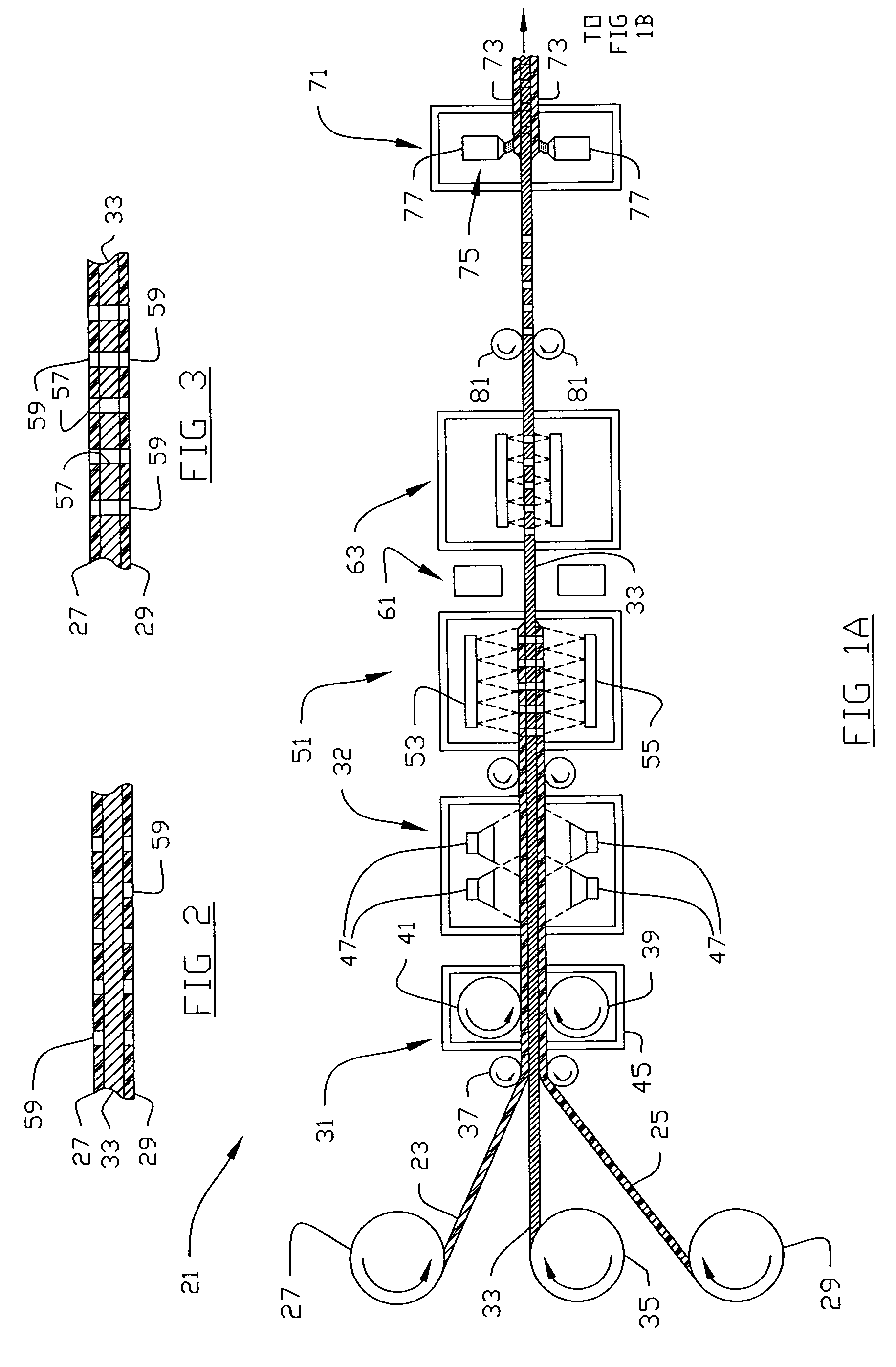
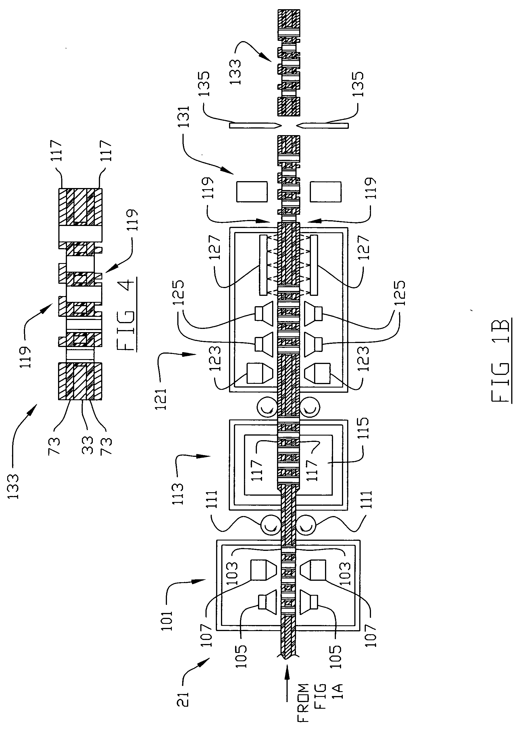
Apparatus and method for making circuitized substrates having photo-imageable dielectric layers in a continuous manner
PatentInactiveUS20060240364A1
Innovation
- A continuous process where conductive and dielectric layers are formed and patterned in a single, solid format, allowing for the creation of conductive thru-holes and circuit patterns using photo-imageable dielectric materials, followed by segmentation to produce individual substrates that can be bonded to form multi-layered structures.

Environmental Regulations for Electronic Materials
The regulatory landscape for electronic materials, particularly photo imageable dielectrics used in high-density applications, has become increasingly stringent as environmental awareness and sustainability concerns continue to grow. Global regulatory frameworks now encompass comprehensive restrictions on hazardous substances, waste management protocols, and lifecycle environmental impact assessments that directly influence the development and deployment of advanced dielectric materials.
The European Union's Restriction of Hazardous Substances (RoHS) directive and Waste Electrical and Electronic Equipment (WEEE) directive establish fundamental compliance requirements for electronic materials. These regulations specifically limit the use of lead, mercury, cadmium, hexavalent chromium, and certain brominated flame retardants in electronic components. For photo imageable dielectrics, this translates to strict material composition requirements and necessitates the development of alternative formulations that maintain performance while meeting environmental standards.
REACH (Registration, Evaluation, Authorization and Restriction of Chemicals) regulation in Europe further complicates the compliance landscape by requiring comprehensive chemical safety assessments for substances used in electronic materials manufacturing. Photo imageable dielectric formulations must undergo extensive testing and documentation to demonstrate their environmental safety profile, including potential impacts on human health and ecosystem integrity.
North American regulations, including EPA guidelines and state-level environmental standards such as California's Proposition 65, impose additional constraints on material selection and manufacturing processes. These regulations particularly focus on volatile organic compound emissions and potential carcinogenic substances commonly found in photopolymer systems used in dielectric applications.
Emerging regulations in Asia-Pacific markets, including China's RoHS implementation and Japan's Green Procurement initiatives, are creating harmonized global standards that manufacturers must navigate. These regulations increasingly emphasize circular economy principles, requiring manufacturers to consider end-of-life material recovery and recycling capabilities in their product design phases.
The regulatory trend toward extended producer responsibility is reshaping how companies approach photo imageable dielectric development, necessitating comprehensive lifecycle assessments and sustainable material sourcing strategies that align with evolving environmental compliance requirements.
Cost-Performance Analysis of High Density PID Solutions
The cost-performance analysis of high-density Photo Imageable Dielectric (PID) solutions reveals significant variations across different implementation approaches. Traditional photolithographic PID processes typically require initial capital investments ranging from $2-5 million for advanced equipment, including high-resolution exposure systems and specialized development chambers. However, these systems demonstrate superior performance metrics with feature resolution capabilities down to 10-15 micrometers and excellent dimensional stability.
Manufacturing cost structures for high-density PID applications show distinct patterns based on production volume and complexity requirements. Low-volume prototype production exhibits costs of $15-25 per square inch, primarily driven by setup costs and material waste. As production scales increase beyond 10,000 units annually, unit costs decrease substantially to $3-8 per square inch, benefiting from optimized material utilization and process standardization.
Material costs constitute approximately 35-45% of total PID solution expenses, with high-performance photosensitive dielectric materials priced between $180-320 per kilogram. Advanced formulations incorporating nano-fillers for enhanced electrical properties command premium pricing but deliver superior dielectric constants below 3.0 and loss tangents under 0.008, justifying the additional investment for critical applications.
Process efficiency metrics demonstrate that optimized high-density PID workflows achieve throughput rates of 150-200 substrates per hour for standard configurations. Advanced inline processing systems can reach 300+ substrates hourly, though requiring 40-60% higher capital investment. Yield rates for mature high-density processes typically exceed 95% for feature sizes above 20 micrometers, dropping to 85-90% for sub-15 micrometer applications.
Comparative analysis against alternative technologies shows PID solutions offering 20-30% cost advantages over traditional subtractive methods for complex geometries, while maintaining equivalent or superior electrical performance. The total cost of ownership over five-year periods favors PID implementations for applications requiring frequent design iterations or high-density interconnect structures.
Unlock deeper insights with PatSnap Eureka Quick Research — get a full tech report to explore trends and direct your research. Try now!
Generate Your Research Report Instantly with AI Agent
Supercharge your innovation with PatSnap Eureka AI Agent Platform!