Photoelectric Effect Modulation through Core-shell Nanostructures
MAR 19, 20269 MIN READ
Generate Your Research Report Instantly with AI Agent
Patsnap Eureka helps you evaluate technical feasibility & market potential.
Photoelectric Effect and Core-shell Nanostructure Fundamentals
The photoelectric effect represents one of the most fundamental quantum mechanical phenomena, first explained by Albert Einstein in 1905, which earned him the Nobel Prize in Physics. This effect occurs when photons with sufficient energy strike a material surface, causing the emission of electrons. The energy relationship is governed by Einstein's equation E = hν - Φ, where hν represents the photon energy, Φ is the work function of the material, and E is the kinetic energy of the emitted electron. This quantum phenomenon forms the foundation for numerous modern technologies including photovoltaic cells, photodetectors, and image sensors.
The efficiency and characteristics of photoelectric emission are intrinsically linked to material properties, surface conditions, and electronic band structures. Traditional bulk materials often exhibit limitations in terms of tunability and optimization for specific applications. The work function, which determines the minimum photon energy required for electron emission, is typically fixed for a given material, constraining the operational parameters and efficiency of photoelectric devices.
Core-shell nanostructures represent a revolutionary approach to material engineering, consisting of a central core material surrounded by one or more shell layers of different compositions. These architectures typically range from 1 to 100 nanometers in diameter, with shell thicknesses controllable at the atomic level. The core provides structural stability and primary functionality, while the shell layers can be engineered to modify surface properties, protect the core from environmental degradation, or introduce new functionalities.
The unique advantage of core-shell configurations lies in their ability to combine the beneficial properties of different materials within a single nanostructure. This heterostructure approach enables precise control over electronic band alignment, surface chemistry, and optical properties. The interface between core and shell materials creates opportunities for charge transfer, energy level modification, and enhanced light-matter interactions that are not achievable in homogeneous materials.
In the context of photoelectric applications, core-shell nanostructures offer unprecedented opportunities for property modulation. The shell material can be selected to optimize light absorption, modify the effective work function, or enhance electron transport properties. Additionally, quantum confinement effects in nanoscale dimensions can lead to size-dependent optical and electronic properties, providing another dimension for performance optimization.
The synthesis and characterization of core-shell nanostructures require sophisticated techniques including chemical vapor deposition, atomic layer deposition, and solution-based methods. Advanced characterization tools such as transmission electron microscopy, X-ray photoelectron spectroscopy, and ultraviolet photoelectron spectroscopy are essential for understanding the structure-property relationships that govern photoelectric performance in these complex nanomaterials.
Market Demand for Enhanced Photoelectric Devices
The global photoelectric device market is experiencing unprecedented growth driven by the increasing demand for high-performance optoelectronic components across multiple industries. Solar energy applications represent the largest segment, where enhanced photoelectric conversion efficiency directly translates to improved energy harvesting capabilities and reduced cost per watt. The renewable energy sector's expansion has created substantial demand for advanced photovoltaic materials that can operate effectively under varying light conditions and environmental stresses.
Consumer electronics constitute another major demand driver, particularly in smartphone cameras, display technologies, and optical sensors. The proliferation of augmented reality, virtual reality, and advanced imaging systems requires photodetectors with superior sensitivity, faster response times, and broader spectral coverage. These applications demand miniaturized devices that maintain high performance while consuming minimal power.
Industrial automation and sensing applications are increasingly relying on sophisticated photoelectric devices for precision manufacturing, quality control, and safety systems. The automotive industry's transition toward autonomous vehicles has generated significant demand for advanced LiDAR systems, infrared sensors, and optical communication components that require enhanced photoelectric performance under challenging operational conditions.
Medical and healthcare applications represent a rapidly growing market segment, where improved photoelectric devices enable more accurate diagnostic equipment, advanced imaging systems, and therapeutic devices. The demand for portable and wearable health monitoring devices has intensified the need for highly sensitive, low-power photodetectors capable of operating across multiple wavelengths.
Telecommunications infrastructure modernization, particularly the deployment of fiber-optic networks and high-speed data transmission systems, continues to drive demand for enhanced photoelectric components. The emergence of quantum communication technologies and advanced optical computing applications further amplifies the need for devices with superior photoelectric properties.
Environmental monitoring and scientific instrumentation sectors require photoelectric devices with exceptional stability, precision, and spectral selectivity. Climate research, pollution monitoring, and space exploration applications demand components that can operate reliably under extreme conditions while maintaining consistent performance over extended periods.
The convergence of these market demands has created a compelling business case for developing enhanced photoelectric devices through innovative approaches such as core-shell nanostructures, which promise to address multiple performance limitations simultaneously across diverse application domains.
Current Challenges in Photoelectric Effect Modulation
The photoelectric effect modulation through core-shell nanostructures faces several fundamental challenges that significantly impact the development and practical implementation of these advanced materials. One of the primary obstacles lies in achieving precise control over the interface quality between core and shell materials. The heterojunction formed at this interface is critical for charge separation and transfer efficiency, yet maintaining atomically sharp interfaces without defects, interdiffusion, or lattice mismatch remains technically demanding across different material combinations.
Scalability represents another major constraint limiting the widespread adoption of core-shell nanostructures for photoelectric applications. While laboratory-scale synthesis methods can produce high-quality nanoparticles with well-defined morphologies, translating these processes to industrial-scale production while maintaining uniformity, size distribution, and structural integrity poses significant manufacturing challenges. The cost-effectiveness of large-scale production remains questionable due to complex synthesis procedures and expensive precursor materials.
Material stability under operational conditions presents ongoing difficulties that affect long-term performance reliability. Core-shell nanostructures often suffer from photocorrosion, thermal degradation, and chemical instability when exposed to harsh environmental conditions or prolonged illumination. The shell material, while intended to protect the core, may itself undergo structural changes or chemical reactions that compromise the overall photoelectric performance over time.
Charge transport mechanisms within core-shell architectures introduce additional complexity that is not fully understood or optimized. The multiple interfaces present in these structures can create energy barriers that impede efficient charge carrier movement, leading to increased recombination rates and reduced quantum efficiency. Controlling the band alignment between core and shell materials to facilitate optimal charge separation remains a significant theoretical and practical challenge.
Surface functionalization and integration with device architectures present further obstacles in translating laboratory achievements to practical applications. The surface chemistry of core-shell nanostructures must be carefully engineered to ensure compatibility with electrode materials and electrolytes while maintaining the desired photoelectric properties. Additionally, achieving uniform dispersion and preventing aggregation during device fabrication continues to challenge researchers and manufacturers in this field.
Existing Core-shell Modulation Solutions
01 Core-shell quantum dot structures for enhanced photoelectric conversion
Core-shell nanostructures utilizing quantum dots as the core material with protective shell layers demonstrate enhanced photoelectric conversion efficiency. The shell layer passivates surface defects and reduces non-radiative recombination, while the core provides strong light absorption. This architecture improves charge carrier separation and transport, leading to superior photoelectric performance in devices such as solar cells and photodetectors.- Core-shell quantum dot structures for enhanced photoelectric conversion: Core-shell nanostructures utilizing quantum dots as the core material with protective shell layers demonstrate enhanced photoelectric conversion efficiency. The shell layer passivates surface defects and reduces non-radiative recombination, while the core provides strong light absorption. This architecture improves charge carrier separation and transport, leading to superior photoelectric performance in solar cells and photodetectors.
- Metal-semiconductor core-shell nanostructures for plasmonic enhancement: Core-shell nanostructures combining metallic cores with semiconductor shells exploit plasmonic effects to enhance photoelectric properties. The metallic core generates localized surface plasmon resonance that amplifies the electromagnetic field, increasing light absorption in the semiconductor shell. This configuration significantly improves photocurrent generation and quantum efficiency in optoelectronic devices.
- Perovskite-based core-shell nanostructures for photovoltaic applications: Core-shell architectures incorporating perovskite materials demonstrate exceptional photoelectric conversion capabilities. The core-shell design protects the perovskite from environmental degradation while maintaining high absorption coefficients and charge mobility. These structures exhibit improved stability and efficiency in photovoltaic devices compared to bare perovskite materials.
- Oxide-based core-shell nanostructures for photoelectrochemical applications: Core-shell nanostructures utilizing metal oxide materials in either core or shell positions enable efficient photoelectrochemical conversion. The heterojunction formed at the core-shell interface facilitates charge separation and reduces recombination losses. These structures are particularly effective in water splitting and photocatalytic applications due to their tunable band alignment and enhanced surface area.
- Carbon-based core-shell nanostructures for flexible photoelectric devices: Core-shell nanostructures incorporating carbon-based materials such as graphene or carbon nanotubes provide excellent electrical conductivity and mechanical flexibility. The carbon component serves as an efficient charge transport pathway while the shell material provides photoactive properties. This combination enables the development of flexible and lightweight photoelectric devices with high performance and durability.
02 Metal-semiconductor core-shell nanostructures for plasmonic enhancement
Core-shell nanostructures comprising metallic cores with semiconductor shells exploit plasmonic effects to enhance photoelectric properties. The metallic core generates localized surface plasmon resonance that amplifies the electromagnetic field, increasing light absorption in the semiconductor shell. This configuration enhances photocurrent generation and quantum efficiency in optoelectronic applications.Expand Specific Solutions03 Oxide-based core-shell nanostructures for photocatalytic applications
Core-shell nanostructures featuring oxide materials demonstrate enhanced photoelectric effects for photocatalytic and energy conversion applications. The core-shell architecture facilitates efficient charge separation by creating heterojunctions that promote electron-hole pair generation and reduce recombination. These structures exhibit improved stability and photocatalytic activity under light irradiation.Expand Specific Solutions04 Carbon-based core-shell nanostructures for photoelectric devices
Core-shell nanostructures incorporating carbon-based materials such as graphene or carbon nanotubes as either core or shell components exhibit unique photoelectric properties. The carbon materials provide excellent electrical conductivity and large surface area, while the complementary layer enhances light absorption and charge transfer. This combination results in improved photoresponse and device performance.Expand Specific Solutions05 Perovskite core-shell nanostructures for optoelectronic applications
Core-shell nanostructures utilizing perovskite materials demonstrate exceptional photoelectric properties due to their high absorption coefficients and tunable bandgaps. The shell layer protects the perovskite core from environmental degradation while maintaining efficient charge extraction. These structures show promise for solar cells, light-emitting diodes, and photodetectors with enhanced stability and efficiency.Expand Specific Solutions
Key Players in Nanostructured Photoelectric Materials
The photoelectric effect modulation through core-shell nanostructures represents an emerging technology field in its early development stage, characterized by significant research activity but limited commercial deployment. The market remains nascent with substantial growth potential as applications span from advanced displays to energy harvesting systems. Technology maturity varies considerably across players, with established corporations like Samsung Electronics, Toshiba, and Philips demonstrating advanced integration capabilities in consumer electronics, while research institutions including KIST, Japan Science & Technology Agency, and various universities (Nanjing University, Jilin University, University of California) focus on fundamental breakthroughs. Specialized companies like Nanosys lead in quantum dot commercialization, whereas industrial giants such as BASF and IBM explore materials science applications. The competitive landscape shows a clear division between academic research pioneers advancing core science and industry leaders working toward scalable manufacturing solutions.
Samsung Electronics Co., Ltd.
Technical Solution: Samsung has developed advanced core-shell quantum dot structures for display applications, utilizing CdSe/ZnS and InP/ZnS core-shell nanostructures to enhance photoelectric conversion efficiency. Their technology focuses on optimizing shell thickness and composition to minimize surface defects and improve charge carrier separation. The company has implemented multi-layer shell architectures that provide better passivation of surface states, leading to enhanced photoluminescence quantum yields exceeding 90% and improved stability under continuous illumination. Their core-shell designs incorporate gradient alloying techniques to reduce lattice mismatch and suppress non-radiative recombination pathways.
Strengths: Industry-leading manufacturing capabilities and extensive R&D resources for commercialization. Weaknesses: Heavy reliance on toxic materials like cadmium in some formulations.
Toshiba Corp.
Technical Solution: Toshiba has developed core-shell nanostructure technology for next-generation solar cell applications, utilizing perovskite-based core materials with protective oxide shells. Their approach focuses on enhancing the stability and efficiency of photoelectric conversion through careful engineering of the core-shell interface. The company has achieved power conversion efficiencies exceeding 20% in laboratory demonstrations by optimizing the shell composition to prevent ion migration and moisture ingress. Their core-shell designs incorporate novel passivation layers that reduce surface recombination velocities to below 10 cm/s, significantly improving open-circuit voltage and fill factor. Toshiba's technology also addresses scalability challenges through solution-processable synthesis methods compatible with roll-to-roll manufacturing.
Strengths: Extensive experience in semiconductor device manufacturing and strong materials science capabilities. Weaknesses: Relatively new to the core-shell nanostructure field compared to specialized companies.
Core Innovations in Photoelectric Nanostructure Design
Core-shell nanostructure based photovoltaic cells and methods of making same
PatentInactiveUS20130269762A1
Innovation
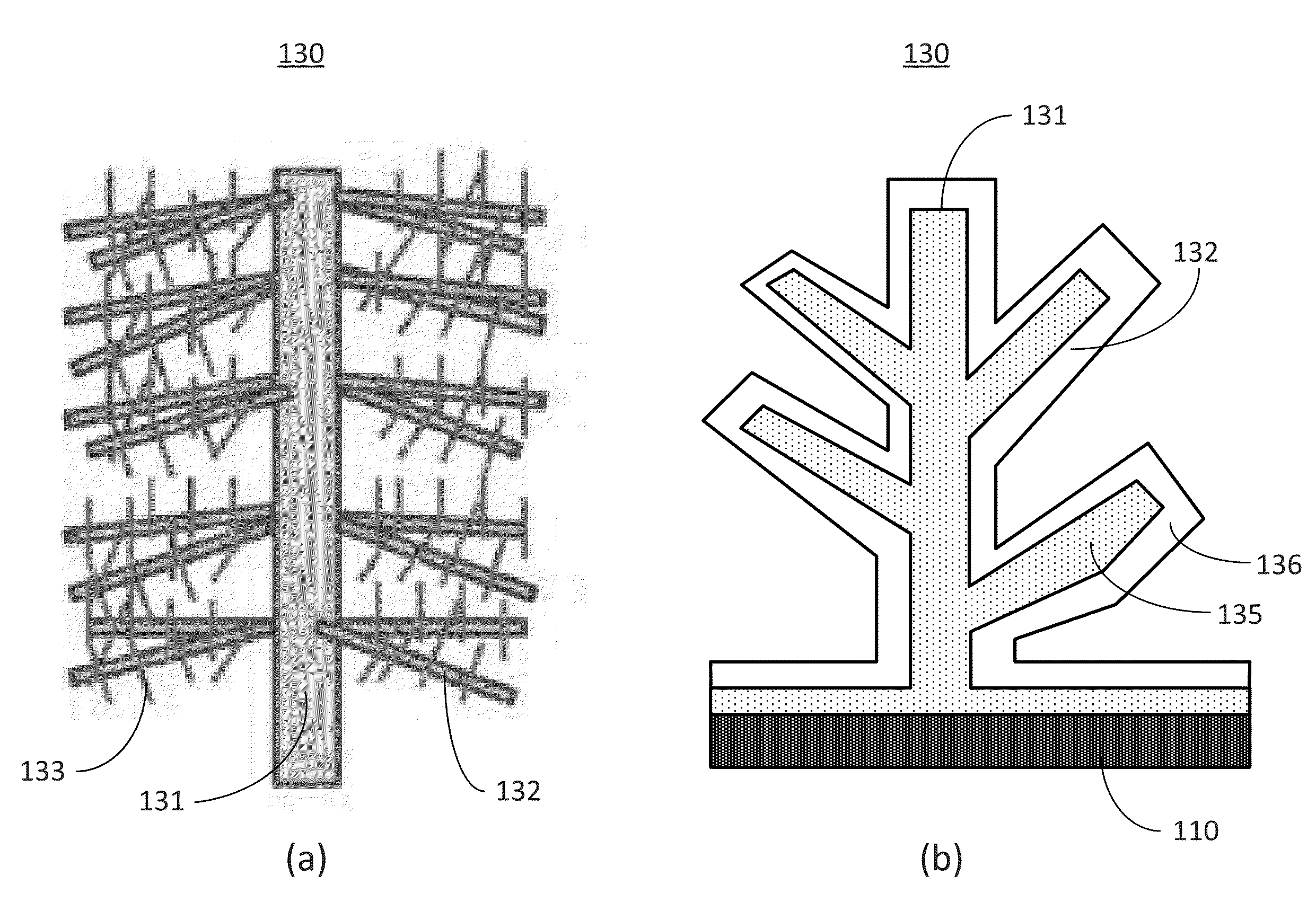
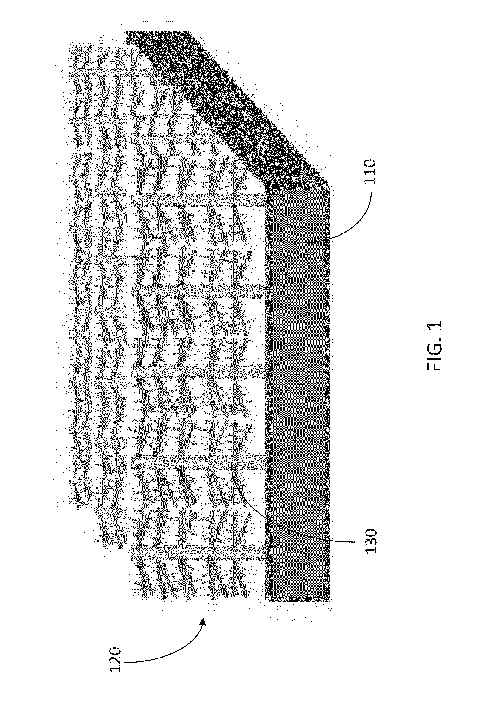
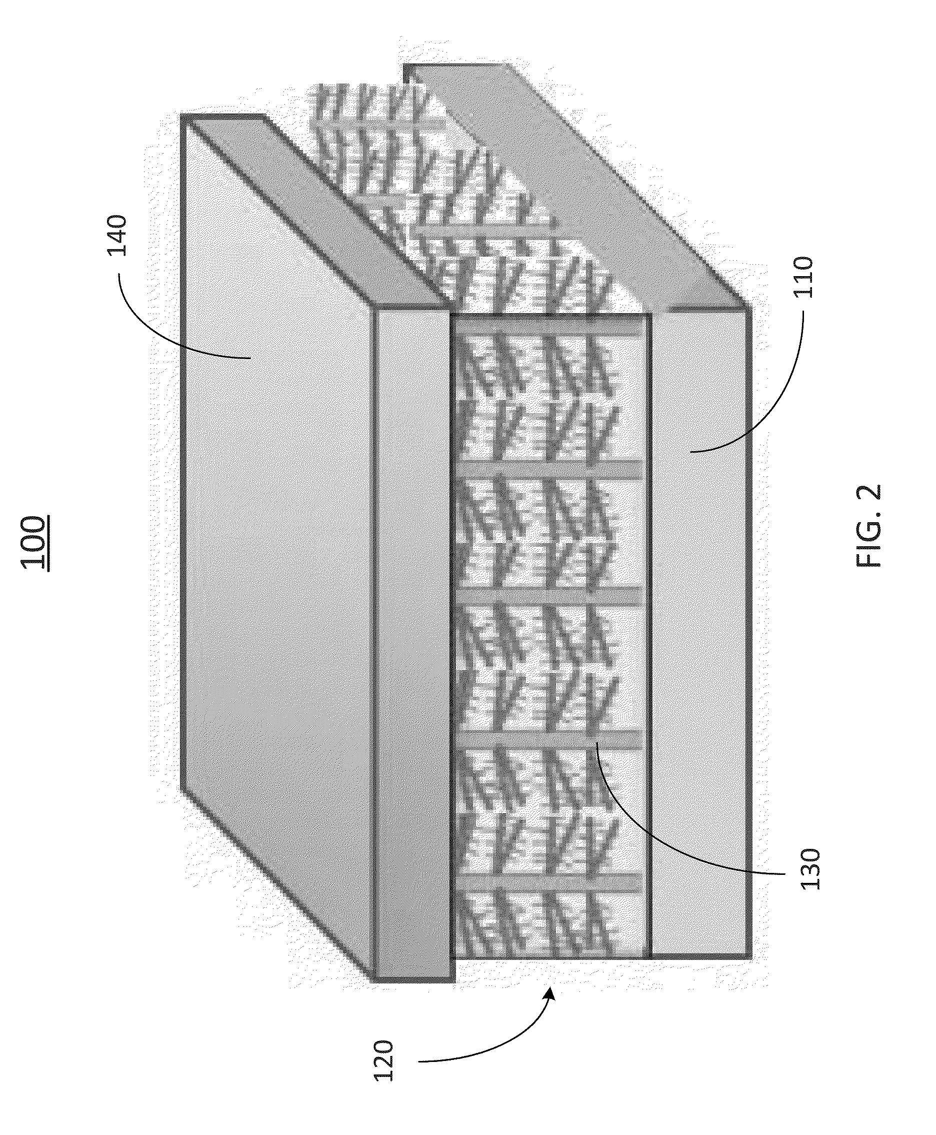
- The development of hierarchical core-shell nanostructures, such as 3D nanotrees or nanobushes with core-shell structures, that enhance light absorption, charge separation, and collection by increasing the p-n junction area and using economic materials and processes for fabrication, including electrochemical and chemical vapor deposition methods.

Core-shell particle, composite, light-receiving member for photoelectric conversion element, and photoelectric conversion element
PatentPendingUS20230171974A1
Innovation
- A core-shell particle structure is developed, comprising an inorganic nanoparticle with a rare earth element and a coating layer of inorganic perovskite, which enhances light wavelength conversion efficiency by minimizing thermal vibration and allowing higher dopant concentrations, thereby improving visible light sensitization characteristics.


Environmental Impact of Nanostructured Materials
The environmental implications of core-shell nanostructures used in photoelectric effect modulation present a complex landscape of both opportunities and challenges. These engineered nanomaterials, while offering unprecedented control over light-matter interactions, introduce novel environmental considerations that require comprehensive assessment across their entire lifecycle.
Manufacturing processes for core-shell nanostructures typically involve high-energy synthesis methods, chemical vapor deposition, and solution-based approaches that consume significant energy and utilize potentially hazardous precursor materials. The production of quantum dots, plasmonic nanoparticles, and semiconductor heterostructures often requires rare earth elements and toxic solvents, creating upstream environmental burdens. Energy-intensive fabrication techniques, including high-temperature annealing and vacuum processing, contribute to the carbon footprint of these advanced materials.
Release pathways into environmental systems occur through multiple routes during manufacturing, application, and end-of-life disposal. Airborne nanoparticles can escape during synthesis and processing operations, while aqueous discharge may contain unreacted precursors and byproducts. Consumer electronics incorporating these nanostructures eventually enter waste streams, potentially releasing engineered nanoparticles into soil and water systems through improper disposal or recycling processes.
Ecological interactions of core-shell nanostructures remain poorly understood, with emerging research indicating complex bioaccumulation patterns and potential toxicity mechanisms. The unique surface chemistry and size-dependent properties of these materials enable them to cross biological barriers and interact with cellular components in unprecedented ways. Aquatic ecosystems appear particularly vulnerable, as nanoparticles can alter photosynthetic processes in algae and accumulate in food webs.
Mitigation strategies are evolving to address these environmental concerns through green synthesis approaches, biodegradable shell materials, and closed-loop manufacturing systems. Researchers are developing water-based synthesis routes, bio-compatible core materials, and recyclable nanostructure designs. Regulatory frameworks are beginning to address nanomaterial-specific environmental standards, though comprehensive guidelines remain under development. Life cycle assessment methodologies specifically tailored for nanostructured materials are becoming essential tools for evaluating and minimizing environmental impact while preserving the technological advantages of these advanced photoelectric systems.
Safety Regulations for Photoelectric Nanomaterials
The development and application of photoelectric nanomaterials incorporating core-shell nanostructures necessitate comprehensive safety regulations to address unique risks associated with their nanoscale properties and photoelectric functionalities. Current regulatory frameworks primarily focus on traditional nanomaterial safety protocols, but the specific characteristics of photoelectric core-shell structures require specialized considerations due to their enhanced surface reactivity and potential for photocatalytic reactions.
International regulatory bodies including the Environmental Protection Agency (EPA), European Chemicals Agency (ECHA), and International Organization for Standardization (ISO) have established foundational guidelines for nanomaterial handling. ISO 12885 provides specific protocols for occupational exposure assessment, while OECD guidelines address environmental release scenarios. However, these existing frameworks inadequately address the unique photoelectric properties and core-shell architectural complexities that can influence toxicity profiles and environmental behavior.
Manufacturing facilities must implement stringent containment protocols during synthesis and processing of photoelectric core-shell nanostructures. Engineering controls include negative pressure environments, high-efficiency particulate air filtration systems, and specialized ventilation designed for nanoparticle containment. Personal protective equipment requirements extend beyond standard protocols to include respiratory protection rated for nanoparticles and anti-static clothing to prevent electrostatic discharge that could affect photoelectric properties.
Workplace exposure limits for photoelectric nanomaterials remain largely undefined, with most regulations defaulting to precautionary approaches based on bulk material properties. The core-shell architecture complicates exposure assessment since different materials in the core versus shell may have distinct toxicological profiles. Emerging research suggests that photoelectric activation under ambient lighting conditions may alter nanoparticle behavior and potential health impacts.
Environmental release regulations require comprehensive lifecycle assessment protocols specific to photoelectric nanomaterials. The photocatalytic activity of these materials can influence their environmental fate and transformation, potentially generating reactive oxygen species or facilitating degradation of co-contaminants. Disposal protocols must account for the persistent photoelectric activity and potential for continued environmental reactivity post-disposal.
Future regulatory development should incorporate real-time monitoring technologies for airborne nanoparticles and establish material-specific exposure limits based on core-shell composition and photoelectric properties rather than relying solely on mass-based metrics.
Unlock deeper insights with Patsnap Eureka Quick Research — get a full tech report to explore trends and direct your research. Try now!
Generate Your Research Report Instantly with AI Agent
Supercharge your innovation with Patsnap Eureka AI Agent Platform!