

Photonics Interposers in AI Infrastructures: Computational Speed
APR 15, 20269 MIN READ
Generate Your Research Report Instantly with AI Agent
PatSnap Eureka helps you evaluate technical feasibility & market potential.
Photonic Interposer AI Infrastructure Background and Objectives
The evolution of artificial intelligence infrastructure has reached a critical juncture where traditional electronic interconnects are becoming the primary bottleneck limiting computational performance. As AI workloads demand increasingly sophisticated processing capabilities, the limitations of copper-based electrical connections in terms of bandwidth, latency, and power consumption have become apparent. Modern AI systems require massive parallel processing capabilities with ultra-high-speed data transfer rates that exceed the physical constraints of conventional electronic architectures.
Photonic interposers represent a paradigm shift in AI infrastructure design, leveraging optical signal transmission to overcome the fundamental limitations of electronic interconnects. These advanced substrates integrate optical waveguides, modulators, and photodetectors directly into the packaging layer, enabling light-based communication between processing units. The technology promises to deliver unprecedented data transfer speeds while significantly reducing power consumption and thermal management challenges that plague current AI accelerator designs.
The historical development of photonic integration has progressed from discrete optical components to sophisticated on-chip photonic circuits. Early implementations focused primarily on telecommunications applications, but recent advances in silicon photonics manufacturing have opened new possibilities for high-performance computing applications. The convergence of mature CMOS fabrication processes with photonic device integration has created viable pathways for cost-effective production of photonic interposers suitable for AI infrastructure deployment.
Current AI computational architectures face severe bandwidth limitations when scaling to exascale performance levels. Graphics processing units and specialized AI accelerators generate enormous amounts of data that must be rapidly exchanged between processing cores, memory systems, and external components. Traditional electrical interconnects suffer from signal integrity issues, crosstalk, and power dissipation problems that worsen with increasing data rates and system complexity.
The primary objective of implementing photonic interposers in AI infrastructures centers on achieving breakthrough computational speeds through optical interconnect technology. This involves developing integrated photonic solutions that can support terabit-per-second data rates with microsecond-level latencies while maintaining energy efficiency standards suitable for large-scale deployment. The technology aims to enable next-generation AI systems capable of processing complex neural network models with unprecedented speed and efficiency, ultimately accelerating artificial intelligence research and commercial applications across multiple industries.
Market Demand for High-Speed AI Computing Solutions
The global AI computing market is experiencing unprecedented growth driven by the exponential increase in computational demands across multiple sectors. Enterprise applications, cloud service providers, and research institutions are increasingly seeking solutions that can handle massive parallel processing workloads with minimal latency. Traditional electronic interconnects are reaching fundamental physical limitations in terms of bandwidth density and power efficiency, creating a critical bottleneck in AI infrastructure performance.
Data centers supporting large language models, computer vision applications, and real-time AI inference are particularly constrained by the speed of inter-chip and inter-board communications. The training of advanced neural networks requires sustained high-bandwidth data movement between processing units, memory systems, and storage arrays. Current copper-based interconnects struggle to maintain signal integrity at the frequencies and distances required for next-generation AI workloads.
The emergence of edge AI applications has further intensified the demand for high-speed computing solutions. Autonomous vehicles, industrial automation systems, and smart city infrastructure require real-time processing capabilities with extremely low latency tolerances. These applications cannot afford the delays introduced by traditional electronic switching and routing systems, particularly when multiple AI accelerators must work in coordination.
Hyperscale cloud providers are actively seeking technologies that can reduce the total cost of ownership while improving computational throughput. Power consumption has become a critical factor, as data centers face increasing pressure to optimize energy efficiency. The heat generation and power requirements of high-speed electronic interconnects represent significant operational challenges that directly impact scalability and profitability.
Photonics interposers address these market demands by offering fundamentally superior bandwidth density and energy efficiency compared to electronic alternatives. The technology enables direct optical communication between processing elements, eliminating the conversion losses and latency penalties associated with electronic switching. This capability is particularly valuable for AI workloads that require frequent data exchange between distributed computing resources.
The market opportunity extends beyond traditional data center applications to include high-performance computing clusters, quantum-classical hybrid systems, and specialized AI inference platforms. Organizations developing custom silicon for AI applications are increasingly recognizing the need for advanced packaging solutions that can fully utilize the computational capabilities of their processors without being limited by interconnect performance.
Current Photonic Integration Challenges in AI Systems
The integration of photonic components into AI systems faces significant thermal management challenges that directly impact computational performance. Silicon photonic devices exhibit temperature-sensitive characteristics, with wavelength drift rates of approximately 0.1 nm per degree Celsius. This sensitivity creates substantial obstacles in maintaining stable optical communication channels within high-density AI accelerator environments where thermal loads can exceed 400W per chip.
Optical coupling efficiency represents another critical bottleneck in current photonic integration approaches. Edge coupling techniques typically achieve 70-80% efficiency, while grating couplers reach only 30-50% efficiency due to fundamental mode mismatch issues. These losses compound across multiple interconnection points, significantly degrading overall system performance and limiting the scalability of photonic interposer architectures in large-scale AI infrastructures.
Manufacturing precision requirements pose substantial challenges for widespread adoption of photonic interposers. Current fabrication processes demand sub-nanometer alignment tolerances for waveguide coupling, with positional accuracy requirements below 100 nanometers. These stringent specifications increase production costs and reduce yield rates, particularly when integrating multiple photonic dies with electronic components on a single interposer substrate.
Signal integrity degradation emerges as a major concern in hybrid photonic-electronic systems. Crosstalk between adjacent waveguides can reach -20dB in densely packed configurations, while dispersion effects limit bandwidth-distance products. Additionally, nonlinear optical effects such as two-photon absorption and free-carrier absorption introduce signal distortion at high optical power levels required for AI computational tasks.
Power consumption optimization remains a persistent challenge despite photonics' inherent advantages. Laser sources, modulators, and photodetectors collectively consume significant electrical power, with current generation silicon photonic transceivers requiring 3-5 pJ per bit. Thermal tuning mechanisms for wavelength stabilization add additional power overhead, potentially offsetting the energy efficiency gains expected from photonic acceleration.
Packaging complexity significantly impacts the commercial viability of photonic interposers in AI systems. Multi-chip module assembly requires specialized flip-chip bonding techniques, precision fiber attachment, and hermetic sealing to protect sensitive optical components. These packaging requirements increase system complexity and manufacturing costs while introducing potential reliability concerns in demanding datacenter environments.
Standardization gaps across the photonic ecosystem create integration barriers for AI system designers. Lack of unified interface protocols between different vendors' photonic components complicates system-level design and limits interoperability. This fragmentation slows adoption rates and increases development timelines for AI infrastructure providers seeking to implement photonic acceleration solutions.
Existing Photonic Interposer Solutions for AI Acceleration
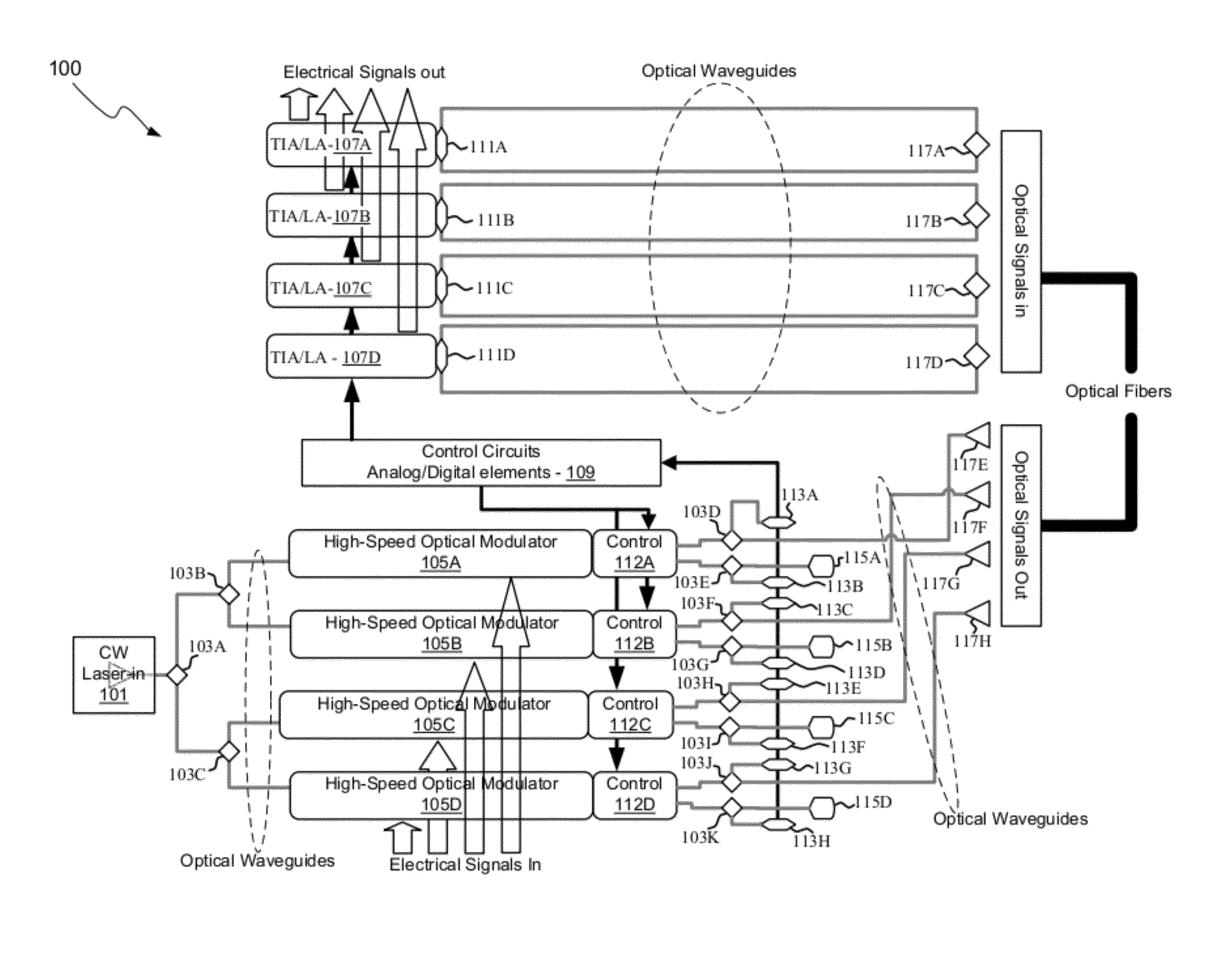
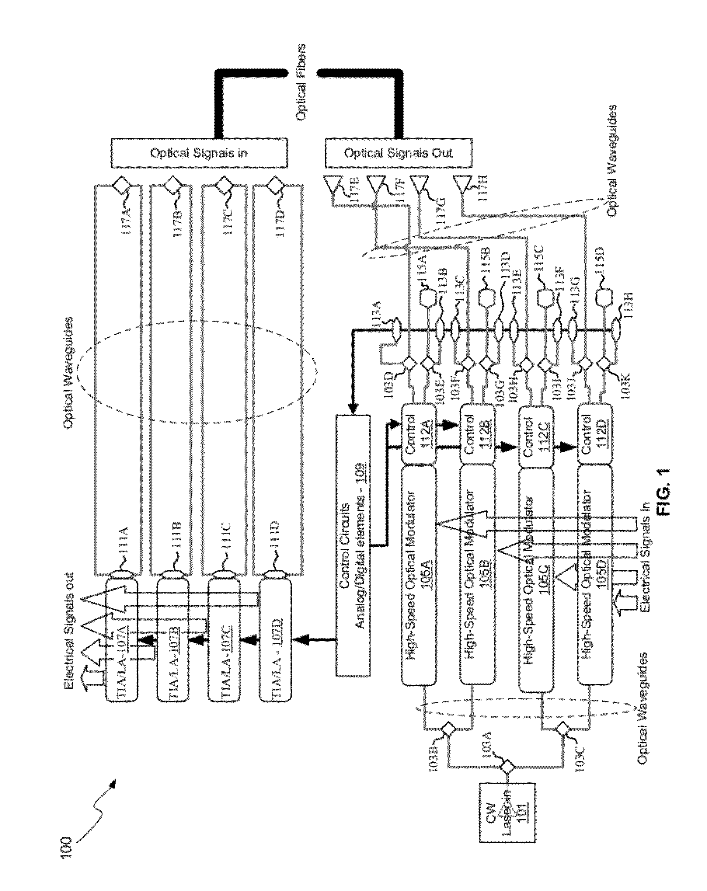
01 Optical interconnect architectures for high-speed data transmission
Photonic interposers utilize optical interconnect architectures to enable high-speed data transmission between components. These architectures incorporate waveguides, optical couplers, and photonic routing structures that facilitate the transfer of data using light signals instead of electrical signals. This approach significantly reduces latency and increases bandwidth, thereby enhancing computational speed in multi-chip systems and data centers.- Optical interconnect architectures for high-speed data transmission: Photonic interposers utilize optical interconnect architectures to enable high-speed data transmission between chips and components. These architectures incorporate waveguides, optical couplings, and photonic routing structures that facilitate faster signal propagation compared to traditional electrical interconnects. The optical pathways reduce latency and increase bandwidth, thereby enhancing overall computational speed in multi-chip modules and integrated systems.
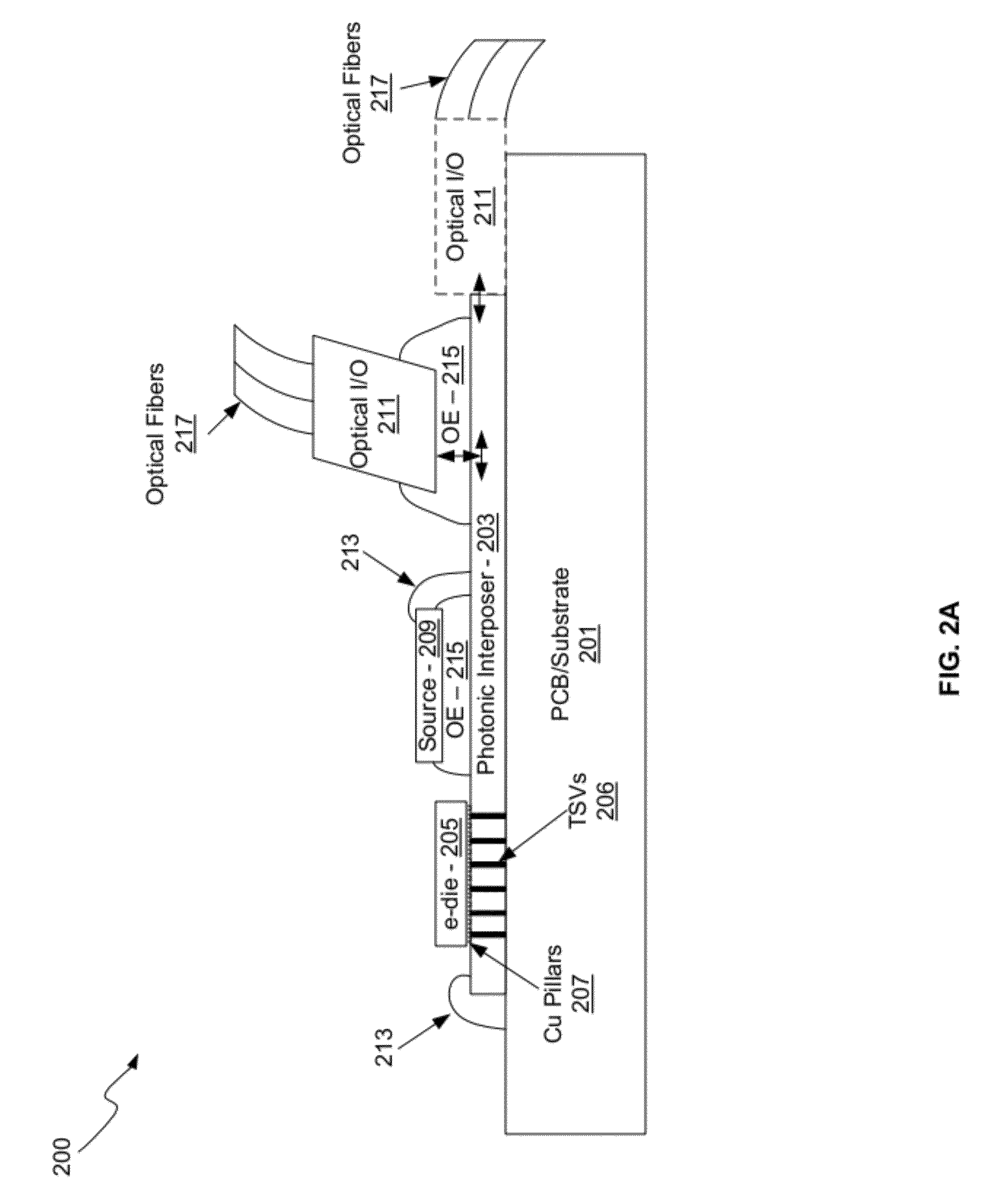
- Integration of photonic and electronic components on interposer substrates: Advanced interposer designs integrate both photonic and electronic components on a single substrate to optimize computational performance. This hybrid integration approach allows for seamless conversion between optical and electrical signals, minimizing conversion losses and signal degradation. The co-location of photonic devices with processing units reduces interconnect distances and improves signal integrity, contributing to enhanced computational speed.
- Use of silicon photonics technology for scalable computing: Silicon photonics technology is employed in interposer designs to achieve scalable and high-performance computing solutions. By leveraging silicon-based optical components such as modulators, detectors, and multiplexers, these interposers enable dense integration and high data rates. The compatibility with standard semiconductor manufacturing processes facilitates cost-effective production while maintaining high computational speeds suitable for data centers and high-performance computing applications.
- Thermal management solutions for photonic interposers: Effective thermal management is critical for maintaining computational speed in photonic interposers. Advanced cooling techniques and thermal interface materials are integrated into interposer designs to dissipate heat generated by high-speed optical and electrical components. Proper thermal control prevents performance degradation due to temperature-induced signal distortion and ensures stable operation at maximum computational speeds.
- Advanced packaging techniques for reduced signal latency: Novel packaging techniques are applied to photonic interposers to minimize signal latency and maximize computational throughput. These techniques include three-dimensional stacking, micro-bump interconnections, and optimized routing layouts that shorten signal paths. By reducing the physical distance signals must travel and improving electrical and optical coupling efficiency, these packaging innovations directly contribute to increased computational speed in complex integrated systems.
02 Integration of photonic and electronic components on interposer substrates
Advanced interposer designs enable the co-integration of photonic devices such as modulators, photodetectors, and lasers with electronic circuits on a single substrate. This hybrid integration approach minimizes signal conversion delays and power consumption while maximizing computational throughput. The interposer acts as a bridge that provides both electrical and optical pathways, enabling seamless communication between heterogeneous components.Expand Specific Solutions03 Wavelength division multiplexing for parallel data processing
Photonic interposers employ wavelength division multiplexing techniques to transmit multiple data streams simultaneously over the same optical channel using different wavelengths of light. This parallel processing capability dramatically increases the aggregate data rate and computational speed. The technology enables dense optical interconnects that support high-performance computing applications requiring massive data throughput.Expand Specific Solutions04 Low-latency optical switching and routing mechanisms
Photonic interposers incorporate fast optical switching elements and routing mechanisms that enable dynamic reconfiguration of data paths with minimal latency. These mechanisms include micro-ring resonators, Mach-Zehnder interferometers, and photonic crossbar switches that can redirect optical signals in nanoseconds or less. The reduced switching time directly contributes to improved computational speed by minimizing communication bottlenecks in complex computing systems.Expand Specific Solutions05 Thermal management and signal integrity optimization
Effective thermal management solutions and signal integrity optimization techniques are critical for maintaining high computational speed in photonic interposers. These include advanced heat dissipation structures, temperature-insensitive photonic components, and signal conditioning circuits that maintain optical signal quality over varying operating conditions. Proper thermal control prevents performance degradation and ensures consistent high-speed operation of the photonic interconnects.Expand Specific Solutions
Key Players in Photonic AI Infrastructure Market
The photonics interposers market for AI infrastructure is in an early growth stage, driven by increasing demand for high-speed, low-latency data transmission in AI workloads. The market shows significant potential as traditional copper interconnects reach bandwidth limitations. Technology maturity varies considerably across players: established semiconductor giants like Intel Corp., Taiwan Semiconductor Manufacturing Co., and Samsung Electronics Co. leverage existing fabrication capabilities, while specialized photonics companies such as Lightmatter Inc., Hyperlume Inc., and AvicenaTech Corp. focus on innovative optical solutions. Research institutions including Tsinghua University, Xidian University, and Georgia Tech Research Corp. contribute foundational technologies. The competitive landscape features a mix of mature foundry providers, emerging photonics specialists, and academic research centers, indicating a technology transition phase where optical interconnects are becoming commercially viable for AI computational acceleration applications.
Lightmatter, Inc.
Technical Solution: Lightmatter develops photonic computing solutions that utilize light-based interconnects to dramatically accelerate AI workloads. Their Passage photonic interconnect technology replaces traditional electrical connections with optical pathways, enabling data centers to achieve significantly higher bandwidth and lower latency. The company's photonic interposers integrate seamlessly with existing AI accelerators, providing up to 10x improvement in interconnect bandwidth while reducing power consumption by 90% compared to electrical alternatives. Their technology specifically addresses the computational speed bottlenecks in large-scale AI training and inference by enabling faster data movement between processors and memory systems.
Strengths: Revolutionary bandwidth improvements and dramatic power reduction in AI interconnects. Weaknesses: Still emerging technology with limited large-scale deployment validation.
Taiwan Semiconductor Manufacturing Co., Ltd.
Technical Solution: TSMC has developed advanced photonic interposer manufacturing capabilities that enable the integration of optical and electronic components for AI acceleration applications. Their technology platform supports the fabrication of complex photonic circuits alongside traditional semiconductor devices, enabling customers to create high-performance AI systems with optical interconnects. TSMC's photonic interposers provide the foundation for next-generation AI chips that require ultra-high bandwidth communication between processing elements. The manufacturing process allows for precise integration of waveguides, modulators, and detectors directly onto silicon substrates, enabling computational speeds that significantly exceed traditional electronic-only solutions for AI workloads requiring massive parallel data processing.
Strengths: World-class semiconductor manufacturing expertise and established customer relationships. Weaknesses: Primarily a foundry service provider rather than system solution developer.
Core Innovations in Photonic-Electronic Integration
Photonics interposer optoelectronics
PatentWO2018098146A1
Innovation
- A photonics interposer system is developed, featuring a substrate with through vias and wires for signal distribution, integrated photonics devices, and precision alignment features like hard stop material layers and metal stacks, allowing for precise attachment and reduced signal loss between components.


Method And System For A Photonic Interposer
PatentActiveUS20120177381A1
Innovation
- A photonic interposer system that integrates silicon photonic devices with CMOS electronics, using Mach-Zehnder interferometer modulators, photodetectors, and grating couplers to process and transmit continuous-wave optical signals, enabling high-speed communication through optical waveguides and copper pillars, allowing independent optimization of electronic and photonic performance.

Standardization Framework for Photonic AI Components
The development of photonic AI components requires a comprehensive standardization framework to ensure interoperability, performance consistency, and scalable deployment across diverse AI infrastructure environments. Current photonic interposer technologies face significant challenges due to the absence of unified standards governing component specifications, interface protocols, and performance metrics.
Existing standardization efforts primarily focus on traditional photonic components rather than AI-specific applications. The IEEE 802.3 standards for optical networking and the Optical Internetworking Forum specifications provide foundational guidelines, but lack provisions for the unique requirements of AI computational workloads. These gaps create compatibility issues between different vendors' photonic interposers and limit the potential for widespread adoption in AI data centers.
A robust standardization framework must address multiple technical dimensions including optical signal formats, wavelength allocation schemes, and thermal management protocols. The framework should establish standardized connector types, power consumption benchmarks, and latency specifications tailored to AI inference and training operations. Additionally, standardized testing methodologies are essential for validating computational speed improvements and ensuring consistent performance across different deployment scenarios.
Industry collaboration between major technology companies, research institutions, and standards organizations is crucial for developing effective photonic AI component standards. The framework should incorporate modular design principles that allow for future technological advances while maintaining backward compatibility. This approach enables manufacturers to innovate within established parameters while ensuring system-level integration remains feasible.
Implementation of standardized photonic AI components would significantly accelerate market adoption by reducing integration complexity and development costs. The framework should also address security considerations, including optical signal encryption standards and tamper-resistant design requirements. Furthermore, environmental sustainability metrics should be integrated into the standardization process to promote energy-efficient photonic solutions that align with modern data center sustainability goals.
Thermal Management in High-Speed Photonic Systems
Thermal management represents one of the most critical engineering challenges in high-speed photonic systems, particularly as photonic interposers become integral to AI infrastructure demanding unprecedented computational speeds. The fundamental issue stems from the inherent heat generation in photonic components, where optical-to-electrical conversions, laser operations, and high-frequency switching create substantial thermal loads that can severely impact system performance and reliability.
In photonic interposers designed for AI applications, thermal effects manifest in multiple ways that directly compromise computational speed. Temperature fluctuations cause wavelength drift in laser sources, leading to crosstalk between optical channels and reduced signal integrity. Silicon photonic waveguides experience refractive index variations with temperature changes, resulting in phase errors that degrade the performance of optical computing elements such as Mach-Zehnder interferometers and ring resonators used in neural network implementations.
The challenge intensifies when considering the dense integration requirements of AI photonic systems. Modern photonic interposers must accommodate thousands of optical components within compact form factors, creating hotspots that can exceed 100°C in localized regions. These temperature gradients not only affect individual component performance but also introduce thermal crosstalk between adjacent optical elements, fundamentally limiting the achievable computational parallelism.
Current thermal management approaches in high-speed photonic systems employ multi-layered strategies combining passive and active cooling techniques. Passive methods include optimized heat sink designs, thermal interface materials with enhanced conductivity, and strategic component placement to minimize thermal coupling. Advanced materials such as diamond heat spreaders and graphene-based thermal interface materials are increasingly deployed to address the unique thermal conductivity requirements of photonic systems.
Active thermal management solutions incorporate micro-channel cooling systems, thermoelectric coolers, and real-time temperature monitoring with feedback control. These systems maintain critical components within specified temperature ranges, typically ±1°C for precision photonic elements. However, the power consumption of active cooling systems can represent up to 30% of total system power in high-performance photonic AI accelerators, creating a significant efficiency trade-off.
Emerging thermal management innovations focus on co-design approaches that integrate thermal considerations into the photonic system architecture from the initial design phase. This includes thermally-aware optical routing algorithms, temperature-compensated photonic circuit designs, and novel packaging techniques that provide superior thermal pathways while maintaining optical performance requirements for next-generation AI computational systems.
Unlock deeper insights with PatSnap Eureka Quick Research — get a full tech report to explore trends and direct your research. Try now!
Generate Your Research Report Instantly with AI Agent
Supercharge your innovation with PatSnap Eureka AI Agent Platform!