Prevent Thermal Mismatch in Layered Substrate-Like PCBs
APR 22, 20269 MIN READ
Generate Your Research Report Instantly with AI Agent
PatSnap Eureka helps you evaluate technical feasibility & market potential.
Thermal Mismatch Background and PCB Design Goals
Thermal mismatch in layered substrate-like PCBs represents one of the most critical reliability challenges in modern electronic systems. This phenomenon occurs when different materials within the PCB structure exhibit varying coefficients of thermal expansion (CTE), leading to mechanical stress, delamination, and potential failure during temperature cycling. As electronic devices become increasingly compact and operate at higher power densities, the thermal management requirements have intensified significantly.
The fundamental issue stems from the multi-material nature of modern PCBs, which typically incorporate copper traces, dielectric substrates, solder masks, and various component attachment materials. Each material responds differently to temperature changes, creating internal stresses that can compromise structural integrity and electrical performance. Traditional FR-4 substrates, while cost-effective, exhibit relatively high CTE values that can mismatch significantly with low-expansion materials like ceramics or certain metal substrates.
Historical development in PCB technology has progressively addressed thermal challenges through material innovations and design methodologies. Early single-layer boards faced minimal thermal mismatch issues, but the evolution toward high-density interconnect (HDI) and embedded component technologies has amplified these concerns. The introduction of thermally conductive substrates and low-CTE materials marked significant milestones in addressing thermal management requirements.
Current PCB design goals center on achieving thermal compatibility across all layers while maintaining electrical performance and manufacturing feasibility. Primary objectives include minimizing CTE differentials between adjacent layers, optimizing thermal conductivity pathways, and ensuring reliable interconnect performance across operational temperature ranges. Design targets typically aim for CTE matching within 2-5 ppm/°C between critical interfaces.
Advanced design strategies now incorporate thermal simulation early in the development process, enabling predictive analysis of thermal stress distributions. The integration of thermal interface materials, strategic via placement for heat dissipation, and careful material selection based on application-specific temperature profiles have become standard practices. These approaches collectively aim to extend product lifespan while maintaining performance reliability under varying thermal conditions.
Market Demand for Reliable Layered PCB Solutions
The global electronics industry faces mounting pressure to deliver increasingly sophisticated devices with enhanced performance, miniaturization, and reliability requirements. This demand directly translates into stringent requirements for printed circuit board solutions, particularly layered substrate-like PCBs that form the backbone of modern electronic systems. The proliferation of high-performance computing, automotive electronics, telecommunications infrastructure, and consumer devices has created an unprecedented need for PCB solutions that can withstand thermal stress while maintaining electrical integrity.
Automotive electronics represents one of the most demanding market segments for reliable layered PCB solutions. Modern vehicles incorporate numerous electronic control units, advanced driver assistance systems, and electric powertrain components that operate under extreme temperature variations. These applications require PCBs capable of maintaining dimensional stability and electrical performance across temperature ranges from sub-zero conditions to elevated engine compartment temperatures. The automotive industry's shift toward electrification and autonomous driving technologies further amplifies the demand for thermally robust PCB solutions.
The telecommunications sector drives substantial demand for reliable layered PCBs, particularly with the ongoing deployment of fifth-generation wireless networks and edge computing infrastructure. Base stations, network switches, and data center equipment generate significant heat loads while requiring uninterrupted operation. These applications necessitate PCB solutions that can manage thermal expansion mismatches between different substrate layers without compromising signal integrity or mechanical reliability.
Consumer electronics manufacturers face intense market pressure to deliver thinner, lighter, and more powerful devices. Smartphones, tablets, laptops, and wearable devices incorporate multiple high-density PCB layers within increasingly compact form factors. The thermal management challenges in these applications are compounded by consumer expectations for reliable performance under diverse environmental conditions, from outdoor temperature extremes to rapid thermal cycling during charging and operation.
Industrial automation and Internet of Things applications create additional market demand for reliable layered PCB solutions. Manufacturing equipment, process control systems, and sensor networks often operate in harsh industrial environments with significant temperature fluctuations, vibration, and chemical exposure. These applications require PCB solutions that maintain long-term reliability while minimizing maintenance requirements and system downtime.
The aerospace and defense sectors represent specialized but high-value market segments with stringent reliability requirements. Avionics systems, satellite communications, and military electronics must operate reliably across extreme temperature ranges while meeting rigorous qualification standards. These applications often justify premium pricing for advanced PCB solutions that demonstrate superior thermal mismatch prevention capabilities.
Market demand is increasingly driven by the total cost of ownership considerations rather than initial component costs alone. System manufacturers recognize that PCB failures due to thermal mismatch can result in expensive warranty claims, field service interventions, and brand reputation damage. This economic reality creates strong market incentives for investing in more reliable layered PCB solutions that prevent thermal-related failures throughout the product lifecycle.
Current Thermal Challenges in Multi-Layer PCB Systems
Multi-layer PCB systems face increasingly complex thermal management challenges as electronic devices demand higher performance density and miniaturization. The fundamental issue stems from the heterogeneous nature of layered substrates, where different materials exhibit varying coefficients of thermal expansion (CTE), thermal conductivity, and heat capacity. This material diversity creates thermal gradients and mechanical stresses that can compromise system reliability and performance.
The primary thermal challenge manifests as localized hotspots formation within the PCB stack-up. High-power components such as processors, power management units, and RF amplifiers generate concentrated heat loads that must be efficiently dissipated through multiple substrate layers. However, the thermal resistance between layers often creates bottlenecks, leading to temperature accumulation and uneven heat distribution across the board surface.
Thermal cycling presents another critical challenge in multi-layer systems. During operational cycles, repeated heating and cooling cause differential expansion and contraction between substrate layers. This mechanical stress can result in delamination, via cracking, and solder joint fatigue. The problem intensifies when combining materials with significantly different CTEs, such as ceramic substrates with organic dielectrics or metal core layers with standard FR-4 materials.
Interlayer thermal interface resistance significantly impacts overall thermal performance. Traditional PCB manufacturing processes often introduce air gaps, adhesive layers, and surface roughness that impede heat transfer between adjacent layers. These thermal barriers become particularly problematic in high-density interconnect designs where multiple substrate types are integrated within a single assembly.
Power density escalation in modern electronics exacerbates existing thermal challenges. Advanced packaging techniques like embedded components and 3D integration increase heat generation per unit volume while reducing available space for thermal management solutions. This trend demands innovative approaches to thermal design that go beyond conventional heat spreading and dissipation methods.
The emergence of wide bandgap semiconductors and high-frequency applications introduces additional thermal complexity. These technologies operate at elevated temperatures and generate heat in concentrated areas, requiring substrate materials and thermal management strategies specifically designed to handle extreme thermal conditions while maintaining electrical performance and signal integrity throughout the operational temperature range.
Existing Thermal Mismatch Prevention Solutions
01 Use of coefficient of thermal expansion (CTE) matched materials
Selecting substrate materials and component materials with closely matched coefficients of thermal expansion can significantly reduce thermal mismatch issues in layered PCB structures. This approach minimizes stress and warpage during temperature cycling by ensuring that different layers expand and contract at similar rates. Materials such as specific ceramic composites, metal alloys, and engineered polymers can be chosen based on their CTE values to create more thermally stable multilayer assemblies.- Use of coefficient of thermal expansion (CTE) matched materials: Selecting substrate materials and component materials with closely matched coefficients of thermal expansion can significantly reduce thermal mismatch issues in layered PCB structures. This approach minimizes stress and warpage during temperature cycling by ensuring that different layers expand and contract at similar rates. Materials such as specific ceramic composites, metal alloys, and engineered polymers can be chosen based on their CTE values to create more thermally stable multilayer assemblies.
- Implementation of buffer or compliant layers: Incorporating intermediate buffer layers or compliant materials between substrates with different thermal expansion properties can absorb thermal stress and prevent delamination or cracking. These layers act as stress relief zones that accommodate differential expansion without transferring excessive mechanical loads to adjacent layers. Compliant materials may include elastomeric compounds, soft adhesives, or specially designed composite structures that provide flexibility while maintaining electrical connectivity.
- Structural design modifications and via arrangements: Optimizing the physical design of layered substrates through strategic placement of vias, thermal relief patterns, and stress-distribution features can mitigate thermal mismatch effects. Design approaches include using staggered via patterns, implementing thermal relief pads, creating expansion slots, and optimizing layer thickness ratios. These structural modifications help distribute thermal stress more evenly across the substrate and prevent stress concentration at critical interfaces.
- Advanced bonding and adhesive technologies: Employing specialized bonding techniques and adhesive materials designed to accommodate thermal expansion differences can improve the reliability of layered PCB assemblies. These technologies include thermally conductive adhesives with controlled elastic properties, low-stress bonding processes, and adhesive systems that maintain flexibility across wide temperature ranges. The bonding materials can be formulated to provide both mechanical strength and thermal stress accommodation.
- Thermal management and heat dissipation structures: Integrating thermal management features such as heat spreaders, thermal vias, and heat dissipation layers can reduce temperature gradients and minimize thermal mismatch effects in multilayer substrates. These structures help maintain more uniform temperature distribution across different layers, thereby reducing differential thermal expansion. Solutions include embedded heat pipes, metal core layers, thermal interface materials, and optimized copper distribution patterns that enhance heat transfer and reduce localized thermal stress.
02 Implementation of compliant interlayer materials
Incorporating compliant or flexible interlayer materials between rigid substrate layers can absorb thermal stresses caused by CTE mismatches. These buffer layers act as stress relief mechanisms that accommodate differential expansion without causing delamination or cracking. Elastomeric materials, soft adhesives, or specially designed compliant films can be strategically placed within the layer stack to improve thermal cycling reliability.Expand Specific Solutions03 Structural design modifications and via arrangements
Optimizing the physical design of layered substrates through strategic via placement, layer thickness control, and geometric patterns can mitigate thermal mismatch effects. Design techniques include using staggered via patterns, implementing thermal relief structures, and controlling aspect ratios of through-holes and vias. These structural modifications help distribute thermal stresses more evenly across the substrate and prevent stress concentration points that could lead to failure.Expand Specific Solutions04 Application of thermal management coatings and layers
Applying specialized thermal management coatings or incorporating dedicated thermal spreading layers can help manage heat distribution and reduce localized thermal gradients that exacerbate CTE mismatch problems. These solutions include heat-dissipating coatings, thermal interface materials, and embedded heat spreaders that promote more uniform temperature distribution across the layered structure. By reducing temperature differentials, these approaches minimize the driving force behind thermal mismatch stresses.Expand Specific Solutions05 Hybrid substrate construction methods
Employing hybrid construction techniques that combine different substrate technologies or materials in a single assembly can address thermal mismatch challenges. These methods may involve integrating organic and inorganic substrates, using localized reinforcement in high-stress areas, or creating composite structures with graded material properties. Hybrid approaches allow designers to optimize different regions of the substrate for specific thermal and mechanical requirements while maintaining overall structural integrity.Expand Specific Solutions
Key Players in Advanced PCB Manufacturing Industry
The thermal mismatch prevention in layered substrate-like PCBs represents a mature technology domain within the rapidly expanding electronics manufacturing industry, valued at over $400 billion globally. The competitive landscape is dominated by established semiconductor giants including Intel, Samsung Electronics, Taiwan Semiconductor Manufacturing Company, and Texas Instruments, who possess advanced thermal management capabilities through decades of R&D investment. Technology maturity varies significantly across players - while companies like Applied Materials, ASML Netherlands, and STMicroelectronics demonstrate cutting-edge solutions for high-performance applications, emerging players such as Beijing NAURA Microelectronics and specialized firms like Tessera focus on niche packaging innovations. The market exhibits intense competition driven by increasing miniaturization demands in automotive, consumer electronics, and industrial applications, with established players leveraging extensive patent portfolios and manufacturing scale advantages over newer entrants.
Intel Corp.
Technical Solution: Intel employs advanced thermal interface materials (TIMs) and copper-filled through-silicon vias (TSVs) in their layered substrate designs to manage thermal expansion mismatches. Their approach includes using low-CTE (coefficient of thermal expansion) organic substrates combined with silicon interposers, achieving CTE matching within 2-3 ppm/°C. Intel's embedded multi-die interconnect bridge (EMIB) technology utilizes localized silicon bridges embedded in organic substrates, reducing thermal stress while maintaining high-density interconnections. The company also implements advanced underfill materials with tailored CTE properties and employs thermal simulation modeling to optimize layer stack-ups and via placement for minimal thermal-mechanical stress during temperature cycling.
Strengths: Industry-leading packaging technology with proven EMIB solutions, extensive thermal modeling capabilities, strong materials engineering expertise. Weaknesses: High development costs, complex manufacturing processes requiring specialized equipment and materials.
Applied Materials, Inc.
Technical Solution: Applied Materials provides comprehensive equipment solutions for thermal mismatch prevention through their advanced deposition and etching systems used in substrate manufacturing. Their approach focuses on enabling precise control of material properties during substrate fabrication, including plasma-enhanced chemical vapor deposition (PECVD) systems for depositing stress-controlled dielectric layers with tailored CTE properties. The company's ion implantation and thermal processing equipment enables substrate manufacturers to create gradient CTE structures and optimize interlayer adhesion. Applied Materials' metrology solutions provide real-time monitoring of thermal expansion coefficients and stress levels during manufacturing processes. Their integrated process solutions support the development of advanced substrate materials including glass-ceramic composites and polymer-metal hybrid structures specifically designed for thermal mismatch mitigation in high-performance electronic applications requiring temperature stability across wide operating ranges.
Strengths: Leading semiconductor equipment provider with deep process expertise, comprehensive metrology and control capabilities, strong partnerships with substrate manufacturers. Weaknesses: Equipment-focused rather than direct solution provider, dependency on customer adoption of advanced processes, high capital equipment costs may limit accessibility.
Core Innovations in Substrate Thermal Compatibility
Printed circuit board and method for mounting at least one semiconductor chip device
PatentPendingEP4489528A1
Innovation
- A printed circuit board with a layer stack comprising a first layer and a second layer of materials with different coefficients of thermal expansion, forcing the board into a curved shape to alleviate stress on interconnect structures, allowing the use of stiffer low-RF-loss materials without inducing creeping in the interconnects.


Method of fabricating multilayered printed circuit board
PatentInactiveUS20120174393A1
Innovation
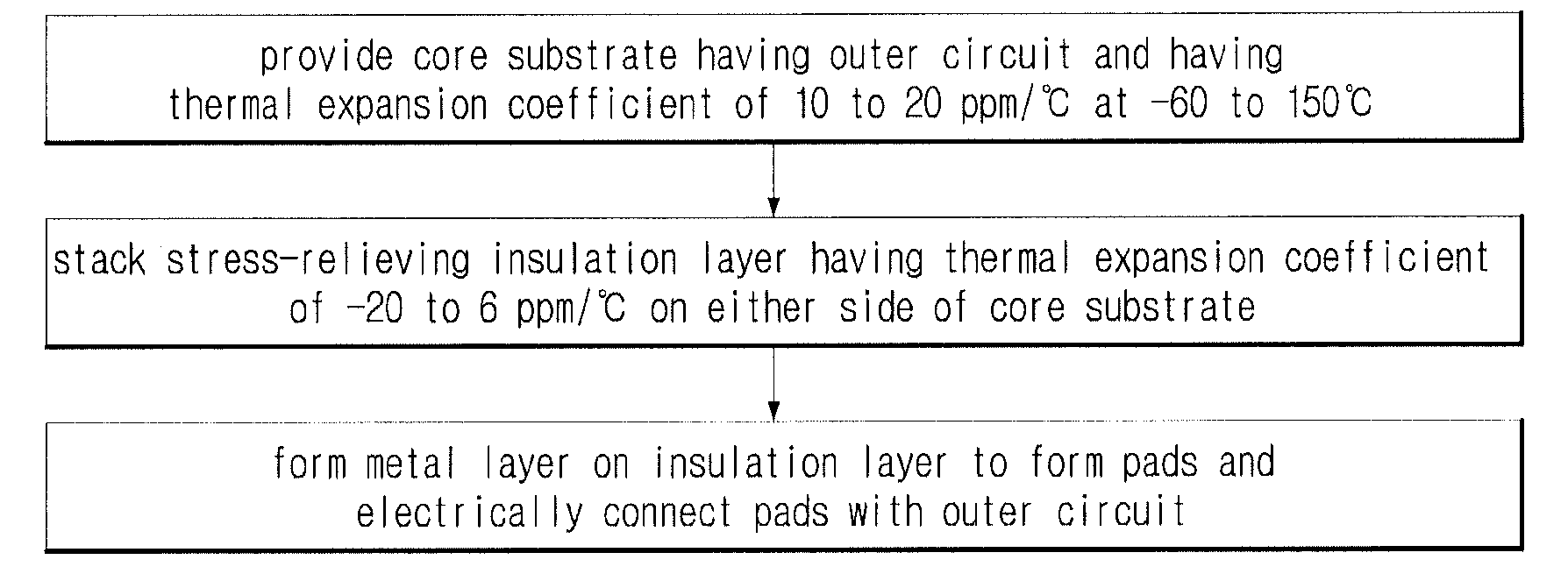
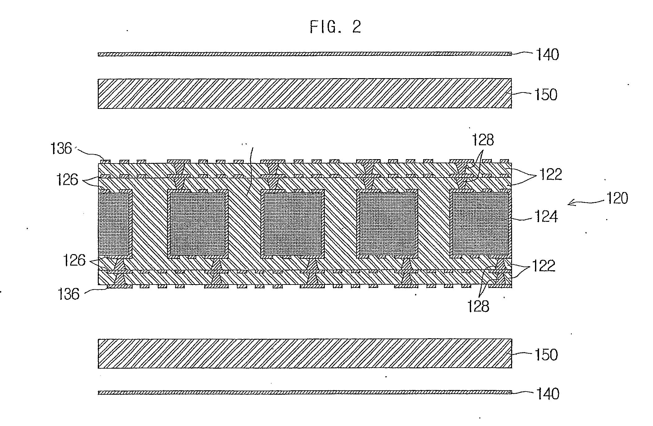
- A method involving a core substrate with a thermal expansion coefficient of 10 to 20 ppm/°C, paired with stress-relieving insulation layers and metal layers having lower thermal expansion coefficients, which are stacked on either side of the core substrate to reduce thermal stress and prevent bending and warping, and pads are formed for electrical connection.

Environmental Standards for Electronic Manufacturing
The electronic manufacturing industry operates under stringent environmental standards that directly impact thermal management strategies for layered substrate-like PCBs. These standards encompass material restrictions, manufacturing process controls, and end-of-life considerations that significantly influence design approaches for preventing thermal mismatch.
RoHS (Restriction of Hazardous Substances) and REACH regulations have fundamentally altered material selection for PCB substrates and thermal interface materials. Lead-free soldering requirements, mandated by these standards, have introduced new thermal expansion challenges as lead-free alloys exhibit different coefficient of thermal expansion properties compared to traditional lead-based solutions. This regulatory shift necessitates careful consideration of substrate material compatibility to prevent thermal stress-induced failures.
WEEE (Waste Electrical and Electronic Equipment) directives impose recyclability requirements that affect substrate material choices and layer construction methods. Manufacturers must balance thermal performance optimization with material separability and recycling feasibility, often leading to design compromises that require innovative thermal management approaches.
ISO 14001 environmental management standards drive manufacturing facilities toward energy-efficient production processes, influencing thermal curing profiles and lamination procedures for multi-layer substrates. These process modifications can affect interlayer adhesion properties and thermal stress distribution, requiring adjusted design parameters to maintain thermal mismatch prevention effectiveness.
Conflict minerals regulations impact sourcing of certain metals used in thermal vias and heat spreaders, forcing manufacturers to explore alternative materials with potentially different thermal properties. This regulatory pressure accelerates development of novel thermal management solutions using compliant materials.
PFAS (Per- and Polyfluoroalkyl Substances) restrictions increasingly limit fluorinated polymer options traditionally used in high-performance substrate applications. These materials often provided excellent thermal stability and low thermal expansion characteristics, necessitating development of alternative substrate formulations that maintain thermal mismatch prevention capabilities while meeting environmental compliance requirements.
Regional variations in environmental standards, such as China's National Standard GB and European EN standards, create additional complexity for global manufacturers. These varying requirements often demand flexible thermal management designs that can accommodate different material specifications while maintaining consistent thermal performance across manufacturing locations.
Reliability Testing Methods for Thermal Cycling
Thermal cycling testing represents the cornerstone methodology for evaluating PCB reliability under temperature-induced stress conditions. This testing approach subjects layered substrate-like PCBs to repeated temperature fluctuations that simulate real-world operational environments, enabling engineers to identify potential failure modes before deployment. The fundamental principle involves exposing test specimens to predetermined temperature ranges while monitoring structural integrity and electrical performance parameters.
Standard thermal cycling protocols typically employ temperature ranges from -40°C to +125°C, with transition rates varying between 5°C to 15°C per minute depending on application requirements. The dwell time at extreme temperatures usually ranges from 15 to 30 minutes, allowing complete thermal equilibration throughout the PCB structure. Test duration commonly extends from 500 to 3000 cycles, with failure criteria established based on electrical continuity, insulation resistance, and visual inspection parameters.
Advanced testing methodologies incorporate real-time monitoring systems that track critical parameters during cycling operations. Resistance measurement techniques enable continuous assessment of interconnect integrity, while high-resolution imaging systems detect micro-crack formation and delamination onset. Digital image correlation methods provide quantitative strain field analysis, revealing stress concentration areas that may lead to premature failure.
Accelerated thermal cycling approaches utilize elevated temperature differentials and increased cycling frequencies to compress testing timeframes while maintaining correlation with field performance. The Arrhenius acceleration model guides temperature selection, ensuring that failure mechanisms remain consistent with normal operating conditions. Coffin-Manson relationships help establish cycle count equivalencies between accelerated and real-world conditions.
Specialized test fixtures accommodate various PCB configurations while ensuring uniform temperature distribution across test specimens. Thermal interface materials and controlled airflow systems minimize temperature gradients that could introduce testing artifacts. Data acquisition systems capture electrical and mechanical responses with sufficient resolution to detect early-stage degradation phenomena, enabling predictive reliability assessments for layered substrate architectures.
Unlock deeper insights with PatSnap Eureka Quick Research — get a full tech report to explore trends and direct your research. Try now!
Generate Your Research Report Instantly with AI Agent
Supercharge your innovation with PatSnap Eureka AI Agent Platform!