

Preventing Yield Loss Through Advanced Wafer Metrology Analytics
MAY 19, 20269 MIN READ
Generate Your Research Report Instantly with AI Agent
PatSnap Eureka helps you evaluate technical feasibility & market potential.
Wafer Metrology Analytics Background and Yield Goals
Wafer metrology has evolved from basic dimensional measurements to sophisticated analytical systems that monitor critical parameters throughout semiconductor manufacturing processes. The semiconductor industry's relentless pursuit of smaller geometries and higher device densities has driven the development of increasingly precise measurement technologies. Traditional metrology approaches focused primarily on post-process inspection, but modern manufacturing demands real-time monitoring and predictive analytics to maintain yield targets.
The evolution of wafer metrology analytics represents a paradigm shift from reactive to proactive manufacturing control. Early metrology systems provided basic feedback on process variations, while contemporary advanced analytics platforms integrate machine learning algorithms, statistical process control, and predictive modeling to anticipate potential yield-limiting conditions before they manifest as defective devices.
Current semiconductor manufacturing faces unprecedented challenges in maintaining yield rates above 90% while scaling to sub-5nm process nodes. Advanced wafer metrology analytics addresses critical pain points including process drift detection, equipment health monitoring, and early identification of systematic defects that could propagate through multiple process steps.
The primary technical objectives center on developing comprehensive measurement strategies that capture both traditional critical dimensions and emerging parameters such as edge placement error, line width roughness, and three-dimensional profile characteristics. These measurements must achieve sub-nanometer precision while maintaining high throughput compatible with volume manufacturing requirements.
Yield optimization goals encompass multiple dimensions of manufacturing performance. The immediate objective involves reducing scrap rates by implementing real-time process adjustments based on metrology feedback. Long-term goals include establishing predictive maintenance schedules for process equipment and developing robust process windows that accommodate natural manufacturing variations without compromising device performance.
Advanced analytics platforms aim to integrate data from multiple metrology tools across different process steps, creating comprehensive process signatures that enable early detection of yield-limiting trends. The ultimate goal involves achieving autonomous manufacturing control where metrology analytics automatically trigger corrective actions without human intervention, thereby minimizing the time between detection and correction of process deviations.
Market Demand for Advanced Semiconductor Yield Solutions
The semiconductor industry faces unprecedented pressure to maximize wafer yield as device geometries continue to shrink and manufacturing complexity increases. Advanced wafer metrology analytics has emerged as a critical solution to address yield loss challenges, driving substantial market demand across the global semiconductor ecosystem.
Market demand for advanced semiconductor yield solutions is primarily fueled by the economic imperative of yield optimization. As wafer fabrication costs escalate with each technology node advancement, even marginal improvements in yield translate to significant financial benefits. Foundries, integrated device manufacturers, and fabless companies are increasingly investing in sophisticated metrology systems that can detect defects and process variations at nanometer scales before they impact final device performance.
The proliferation of artificial intelligence, 5G communications, and Internet of Things applications has intensified demand for high-performance semiconductors with stringent quality requirements. These applications cannot tolerate the yield variability associated with traditional manufacturing approaches, necessitating advanced analytics capabilities that can predict and prevent yield excursions in real-time.
Memory manufacturers represent a particularly strong market segment, as their products require exceptional uniformity across large wafer areas. The transition to 3D NAND and advanced DRAM architectures has created new metrology challenges that conventional inspection methods cannot adequately address, driving adoption of machine learning-enhanced analytics platforms.
Automotive semiconductor applications have introduced additional market dynamics, with zero-defect requirements pushing manufacturers toward comprehensive yield monitoring solutions. The automotive industry's emphasis on long-term reliability and safety has created demand for metrology systems capable of detecting latent defects that might not manifest until after extended operation periods.
Geographically, the market shows strong concentration in regions with significant semiconductor manufacturing presence. Asian markets, particularly Taiwan, South Korea, and China, demonstrate robust demand driven by major foundry operations and government initiatives supporting domestic semiconductor capabilities. North American and European markets focus more on specialized applications and advanced research and development activities.
The market landscape is characterized by increasing integration between metrology hardware and analytics software, with customers seeking comprehensive solutions rather than standalone tools. This trend reflects the growing recognition that effective yield management requires sophisticated data analysis capabilities that can correlate measurements across multiple process steps and identify subtle patterns indicative of emerging yield issues.
Current Wafer Metrology Challenges and Yield Loss Issues
The semiconductor industry faces unprecedented challenges in maintaining high yield rates as device geometries continue to shrink and manufacturing processes become increasingly complex. Traditional wafer metrology approaches, which rely on periodic sampling and offline measurements, are proving inadequate for detecting subtle process variations that can lead to significant yield losses. These conventional methods often miss critical defects or process deviations that only become apparent after final device testing, resulting in substantial economic losses and reduced manufacturing efficiency.
Process variation control represents one of the most significant challenges in modern wafer fabrication. As feature sizes approach atomic scales, even minor fluctuations in parameters such as critical dimension uniformity, overlay accuracy, and film thickness can cause catastrophic yield impacts. Current metrology systems struggle to provide the spatial resolution and measurement frequency required to detect these variations in real-time, leading to the production of defective wafers that are only identified downstream in the manufacturing process.
Defect detection capabilities of existing metrology infrastructure are increasingly strained by the complexity of advanced node processes. Traditional optical inspection systems face fundamental limitations when attempting to identify defects smaller than the wavelength of light used for inspection. Additionally, the three-dimensional nature of modern device structures creates shadowing effects and measurement artifacts that can mask critical defects or generate false positives, reducing the overall effectiveness of quality control systems.
Data integration and analysis present another major obstacle in current wafer metrology practices. Manufacturing facilities generate enormous volumes of measurement data from multiple metrology tools, but lack the sophisticated analytics capabilities needed to extract actionable insights from this information. The absence of real-time data correlation across different measurement stations prevents operators from identifying systematic issues before they impact yield, resulting in reactive rather than proactive process control.
Equipment throughput limitations further compound these challenges, as high-resolution metrology measurements often require significant time investments that conflict with production volume requirements. The trade-off between measurement accuracy and manufacturing speed forces facilities to make compromises that can leave critical process variations undetected. This situation is exacerbated by the increasing number of process steps required for advanced devices, each requiring dedicated metrology checkpoints.
The economic impact of these metrology limitations is substantial, with yield losses directly translating to reduced profitability and competitive disadvantage. Industry estimates suggest that even small improvements in yield detection and control can result in millions of dollars in annual savings for large-scale manufacturing operations, highlighting the urgent need for advanced metrology analytics solutions.
Existing Advanced Metrology Solutions for Yield Enhancement
01 Wafer defect detection and classification systems
Advanced metrology systems utilize sophisticated algorithms and imaging techniques to detect, classify, and analyze defects on semiconductor wafers. These systems employ pattern recognition, machine learning, and statistical analysis to identify various types of defects that can impact yield. The detection systems can differentiate between critical defects that affect functionality and non-critical defects, enabling more accurate yield predictions and targeted process improvements.- Wafer defect detection and classification systems: Advanced metrology systems utilize sophisticated algorithms and imaging techniques to detect, classify, and analyze defects on semiconductor wafers. These systems employ pattern recognition, machine learning, and statistical analysis to identify various types of defects that can impact yield. The detection systems can differentiate between critical and non-critical defects, enabling targeted process improvements and yield optimization strategies.
- Statistical process control and yield prediction models: Implementation of statistical methods and predictive modeling techniques to analyze wafer metrology data and forecast yield outcomes. These approaches utilize historical data patterns, process parameters, and measurement results to build predictive models that can identify potential yield loss scenarios before they occur. The systems enable proactive process adjustments and optimization strategies based on real-time analytics.
- Real-time process monitoring and feedback control: Advanced monitoring systems that provide continuous surveillance of wafer fabrication processes through integrated metrology tools. These systems collect real-time measurement data and provide immediate feedback to process equipment, enabling dynamic adjustments to maintain optimal processing conditions. The feedback mechanisms help prevent yield loss by detecting process deviations early and implementing corrective actions automatically.
- Multi-dimensional data analysis and correlation techniques: Sophisticated analytical methods that examine relationships between multiple process variables, measurement parameters, and yield outcomes. These techniques involve complex data mining, correlation analysis, and multi-variate statistical methods to identify root causes of yield loss. The analysis helps establish connections between seemingly unrelated process parameters and their cumulative impact on final product yield.
- Automated decision support and optimization algorithms: Intelligent systems that automatically analyze metrology data and provide recommendations for process optimization and yield improvement. These algorithms incorporate artificial intelligence, expert systems, and optimization techniques to suggest specific actions for addressing yield loss issues. The systems can prioritize corrective actions based on their potential impact on overall yield and manufacturing efficiency.
02 Statistical process control and yield modeling
Implementation of statistical methods and mathematical models to correlate metrology data with yield outcomes. These approaches use historical data, real-time measurements, and predictive analytics to establish relationships between process parameters and final yield. Advanced statistical techniques help identify process variations and their impact on device performance, enabling proactive yield management and process optimization.Expand Specific Solutions03 Real-time process monitoring and feedback control
Systems that provide continuous monitoring of wafer fabrication processes with immediate feedback mechanisms to prevent yield loss. These solutions integrate sensors, data acquisition systems, and control algorithms to detect process deviations in real-time. The monitoring systems can automatically adjust process parameters or alert operators to prevent defect formation and maintain optimal manufacturing conditions.Expand Specific Solutions04 Machine learning and artificial intelligence for yield prediction
Application of advanced computational techniques including neural networks, deep learning, and artificial intelligence algorithms to analyze complex metrology datasets for yield prediction. These systems can process large volumes of measurement data to identify subtle patterns and correlations that traditional analysis methods might miss. The predictive capabilities enable early detection of yield-limiting factors and optimization of manufacturing processes.Expand Specific Solutions05 Integrated metrology and process optimization platforms
Comprehensive platforms that combine multiple metrology techniques with process optimization tools to minimize yield loss. These integrated systems coordinate various measurement technologies, data analysis methods, and process control strategies to provide holistic yield management solutions. The platforms enable seamless data flow between different manufacturing stages and facilitate coordinated optimization efforts across the entire fabrication process.Expand Specific Solutions
Key Players in Semiconductor Metrology and Analytics
The advanced wafer metrology analytics market for yield loss prevention represents a mature yet rapidly evolving sector driven by increasing semiconductor complexity and shrinking process nodes. The industry spans from established foundries like TSMC and Samsung Electronics to specialized equipment providers such as KLA Corp and Applied Materials, who lead in metrology solutions. Technology maturity varies significantly across players - while foundries like TSMC and SMIC demonstrate advanced implementation capabilities, emerging companies like Dongfang Jingyuan Electron and PDF Solutions focus on AI-driven analytics and specialized yield management software. The competitive landscape includes memory manufacturers (SK Hynix, Micron Technology), EDA software providers (Synopsys), and metrology equipment specialists, creating a comprehensive ecosystem where traditional hardware approaches increasingly integrate with machine learning and data analytics platforms to address next-generation yield optimization challenges.
Taiwan Semiconductor Manufacturing Co., Ltd.
Technical Solution: TSMC has developed proprietary advanced process control (APC) systems that integrate comprehensive wafer metrology with predictive analytics to minimize yield loss. Their approach combines high-density sampling across wafers with machine learning models that analyze patterns in critical dimensions, overlay accuracy, and film properties. The company utilizes automated optical inspection systems coupled with scanning electron microscopy for defect detection and classification. TSMC's metrology strategy includes real-time statistical process control that monitors key parameters such as line width roughness, sidewall angles, and material composition variations. Their integrated data management system correlates metrology results with process tool performance, enabling predictive maintenance and proactive yield optimization across their advanced node manufacturing processes.
Strengths: Extensive manufacturing experience and advanced node expertise with proven yield optimization. Weaknesses: Proprietary solutions may have limited applicability outside TSMC's specific processes.
KLA Corp.
Technical Solution: KLA Corporation provides comprehensive wafer metrology solutions through their advanced inspection and measurement systems. Their technology includes optical and e-beam inspection tools that detect defects at nanometer scales, combined with machine learning algorithms for predictive analytics. The company's Process Watch software platform integrates real-time monitoring with historical data analysis to identify yield-limiting patterns before they impact production. Their solutions feature automated defect classification, statistical process control, and advanced overlay metrology that enables sub-nanometer precision measurements. KLA's systems can detect critical dimension variations, film thickness irregularities, and contamination issues across the entire wafer surface, providing actionable insights to prevent yield loss through early intervention and process optimization.
Strengths: Industry-leading detection sensitivity and comprehensive metrology portfolio. Weaknesses: High equipment costs and complex system integration requirements.
Core Innovations in Predictive Wafer Analytics
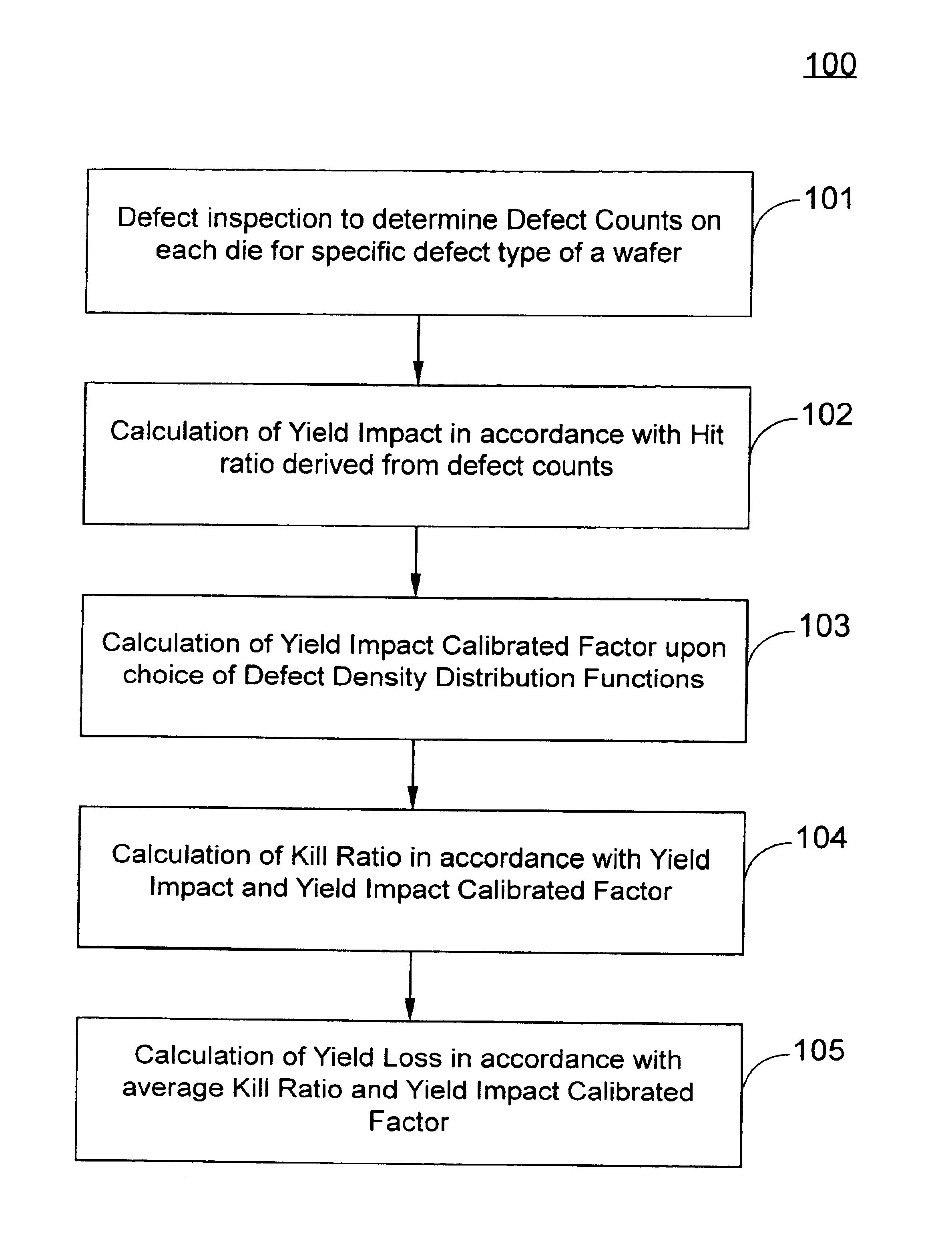
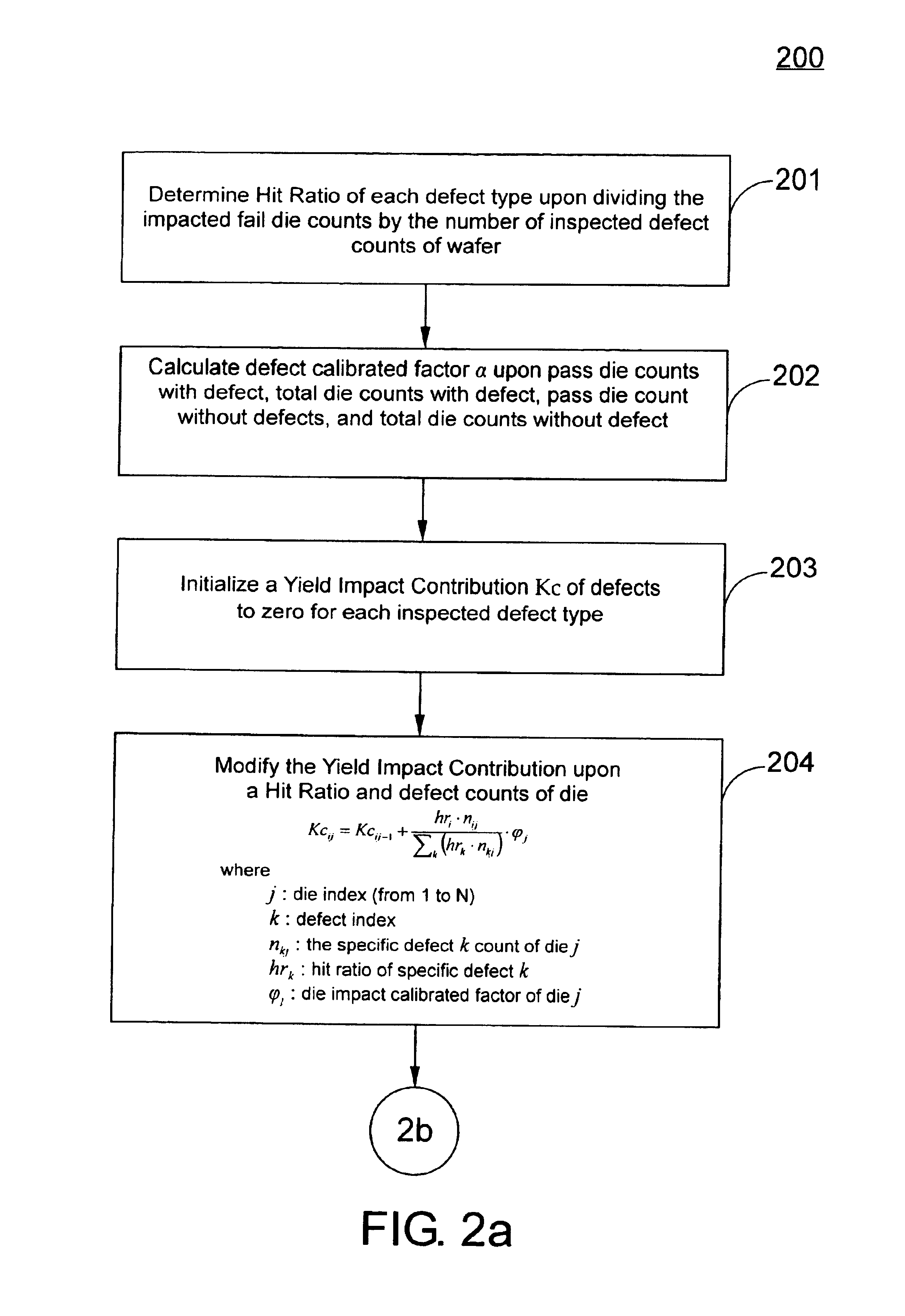
System and method for effective yield loss analysis for semiconductor wafers
PatentInactiveUS6947806B2
Innovation
- A calibrated method for calculating the 'kill ratio' is introduced, which involves computing yield impact contributions based on defect classification and die-based sampling, using formulas to weight hit ratios and defect counts, and applying calibrated factors to predict yield loss effectively.

Yield prediction and statistical process control using predicted defect related yield loss
PatentInactiveEP1049153A3
Innovation
- A method that determines killing probabilities based on historic inspection data, classifies defects using inspection parameters, and calculates predicted yield loss using the equation ΔYk = 1-ij(1-kpkijnkij), allowing for real-time yield prediction and statistical process control without manual classification.


Semiconductor Industry Standards and Compliance
The semiconductor industry operates under a comprehensive framework of standards and compliance requirements that directly impact wafer metrology analytics implementation. International standards organizations such as SEMI, IEEE, and ISO have established critical guidelines governing measurement accuracy, data integrity, and process control methodologies. These standards ensure that advanced metrology analytics systems maintain consistent performance across different manufacturing environments and equipment platforms.
SEMI standards, particularly SEMI E125 for equipment data collection and SEMI E164 for manufacturing execution systems, provide foundational requirements for metrology data management. These specifications mandate specific data formats, communication protocols, and quality metrics that advanced analytics platforms must support. Compliance with these standards ensures interoperability between different metrology tools and enables seamless integration of analytics solutions across multi-vendor manufacturing environments.
Quality management systems under ISO 9001 and automotive-specific IATF 16949 standards impose rigorous documentation and traceability requirements on metrology processes. Advanced analytics systems must maintain comprehensive audit trails, calibration records, and measurement uncertainty calculations to meet these compliance obligations. The implementation of statistical process control methodologies must align with established industry practices while incorporating machine learning and artificial intelligence capabilities.
Data security and intellectual property protection represent critical compliance areas for advanced metrology analytics. Standards such as ISO 27001 for information security management and NIST cybersecurity frameworks establish mandatory requirements for protecting sensitive manufacturing data. Analytics platforms must implement robust encryption, access controls, and data governance mechanisms to prevent unauthorized disclosure of proprietary process information.
Regulatory compliance extends to environmental and safety standards, including RoHS directives and REACH regulations, which influence material selection and process monitoring requirements. Advanced metrology analytics must support compliance reporting by tracking material compositions, process parameters, and environmental impact metrics throughout the manufacturing lifecycle.
The emergence of Industry 4.0 and smart manufacturing initiatives has introduced new compliance considerations related to data sovereignty, cross-border data transfers, and algorithmic transparency. Manufacturing organizations must ensure that their advanced analytics implementations comply with regional data protection regulations while maintaining the flexibility to leverage global manufacturing networks and collaborative research partnerships.
Cost-Benefit Analysis of Advanced Metrology Investment
The economic justification for advanced wafer metrology analytics requires a comprehensive evaluation of capital expenditure against potential yield improvements and operational savings. Initial investment costs typically range from $2-5 million for state-of-the-art metrology systems, including hardware acquisition, software licensing, and facility modifications. Additional expenses encompass staff training, system integration, and ongoing maintenance contracts, which can add 15-20% to the total cost of ownership over a five-year period.
Return on investment calculations demonstrate compelling financial benefits when considering yield loss prevention scenarios. Advanced metrology analytics can detect process deviations 2-3 process steps earlier than traditional methods, potentially preventing yield losses of 0.5-2% per wafer lot. For a typical 300mm fab processing 40,000 wafers monthly, this translates to annual savings of $8-15 million, assuming an average selling price of $800 per wafer and current yield rates of 85-90%.
Operational efficiency gains provide additional value streams beyond direct yield improvements. Reduced rework cycles decrease cycle time by 10-15%, enabling higher throughput without additional capital investment. Enhanced process control capabilities minimize material waste and reduce the frequency of costly equipment downtime events. Statistical analysis indicates that facilities implementing advanced metrology analytics experience 25-30% fewer excursion events requiring engineering intervention.
Risk mitigation represents a critical but often undervalued benefit component. Early detection of systematic process issues prevents cascade failures that could impact entire product lots, potentially avoiding losses exceeding $50 million in extreme scenarios. The ability to maintain tighter process control windows also reduces warranty claims and customer returns, protecting brand reputation and long-term revenue streams.
Payback period analysis typically shows break-even points within 12-18 months for high-volume manufacturing environments. Sensitivity analysis reveals that even conservative yield improvement assumptions of 0.3% generate positive net present value over a five-year investment horizon, making advanced metrology analytics a financially robust strategic investment for semiconductor manufacturers focused on operational excellence.
Unlock deeper insights with PatSnap Eureka Quick Research — get a full tech report to explore trends and direct your research. Try now!
Generate Your Research Report Instantly with AI Agent
Supercharge your innovation with PatSnap Eureka AI Agent Platform!